Note: Descriptions are shown in the official language in which they were submitted.
CA 02824661 2013-08-23
.. ACTIVE MATRIX PIXEL BRIGHTNESS CONTROL
FIELD OF THE DISCLOSURE
..
[0001] The present disclosure generally relates to electronic displays, and
more particularly to
adjusting brightness in active matrix displays.
BACKGROUND
[0002] Advancements in the design of Organic Light Emitting Diode (OLEDs)
displays, such as
Active Matrix OLED (AMOLED) displays, have resulted in an increase in the
variety of
applications that incorporate such display technology. Unlike many other types
of displays, such
as conventional backlit LCD designs, AMOLED devices include light emitters in
each individual
pixel and require no backlight. These individual pixels emit light with
intensity according to a
value programed into that pixel, which causes a proportional electrical
current to be supplied to
the in-pixel OLED device. This OLED current (ToLED) is controlled by circuits
associated with
each pixel, which may include one or more thin film transistors. (TFT). In
other types of
displays that use a backlight to create the light that is emitted by the
display, the display
brightness is able to be easily adjusted by simply changing the intensity of
light emitted by the
backlight of the display. In contrast to adjusting one brightness value that
controls the backlight
intensity for the entire display, adjustment of brightness in an AMOLED
display is accomplished
by modifying the intensity of light emitted by each OLED element in the
display.
[0003] Controlling display brightness is often used to control power
consumption, whereby the
brightness of light emitted by the display is varied in response to ambient
light brightness and
also in response to the content that is being displayed. In displays with a
common backlight,
such as conventional Liquid Crystal Displays (LCDs), algorithms such as
content aware
- 1 -
CA 02824661 2013-08-23
..
brightness/backlight control (CABC) reduce power consumption by
determining limits on pixel
brightness based upon an analysis of the data defining all of the pixels of
the displayed image. In
general, displays with content aware brightness control (CABC) are controlled
by pulse with
modulation (PWM) of the backlight based upon an analysis of the backlight
brightness required
by the image being presented on the display.
[0004] The brightness of an entire AMOLED display is able to be controlled
globally by
controlling the time that each pixel emits light, which is referred to as
"emission time," or by
controlling, e.g., limiting, the electrical current delivered to the pixel
OLED element during the
emission time. Limiting emission time is able to reduce pixel brightness by
shortening the
duration by which all elements of the OLED display are in a light emission
phase. In one
example, a switch is placed between the drive transistor of the pixel and the
OLED element of
the pixel opens after the display has been configured to have each element
emit light at its
programmed intensity. That is to say, the switch, which is able to be
implemented as a Thin
Film Transistor (TFT), is pulsed and the OLED element will only emit light
when the switch is
closed.
[0005] Lowering the brightness of all pixels of an AMOLED display is able to
be performed by
dynamically changing the voltages of the DC power or bias lines supplying all
OLED pixel
elements. In one example, the two polarities of direct current (DC) power
lines supplying power
to the pixels of a display are indicated as EL_VDD and EL_VS S. Lowering the
voltage between
EL _ VDD and EL _VS S causes a reduction in the voltage across the OLED pixel
and thereby
reduces the electrical current passing through the pixel and thereby lowers
the brightness of the
entire display.
- 2 -
CA 02824661 2013-08-23
-
[0006] In order to achieve desired aesthetics when performing the above
described brightness
control mechanisms, an analysis of the relationships of the intensity of each
pixel in an image to
be displayed is performed in order to determine an effective amount of overall
display brightness
reduction given the image data to be displayed. In general, specialized
circuitry or other image
processing resources are used to perform this image frame data analysis. Such
additional
processing adds complexity to the associated display driver or controller
circuitry of a display.
[0007] Therefore, the operation of circuits used to reduce display brightness
in active matrix
displays with emissive pixel elements increases the cost and complexity of
such circuits, thereby
limiting the inclusion of energy conserving brightness control circuits in
such displays.
BRIEF DESCRIPTION OF THE DRAWINGS
[0008] The accompanying figures where like reference numerals refer to
identical or
functionally similar elements throughout the separate views, and which
together with the detailed
description below are incorporated in and form part of the specification,
serve to further illustrate
various embodiments and to explain various principles and advantages all in
accordance with the
present disclosure, in which:
[0009] FIG. 1 illustrates a handheld communications device, according to one
example;
[0010] FIG. 2 illustrates an Active Matrix Organic Light Emitting Diode
(AMOLED) display
component diagram, according to one example;
[0011] FIG. 3 illustrates an Active Matrix Organic Light Emitting Diode
(AMOLED) display
pixel circuit diagram, according to one example;
- 3 -
CA 02824661 2013-08-23
-
[0012] FIG. 4 illustrates a programming time interval signal timing
diagram, according to one
example;
[0013] FIG. 5 illustrates a display brightness reduction signal diagram,
according to one
example;
[0014] FIG. 6 illustrates a brightness reduction emission comparison diagram,
according to one
example;
[0015] FIG. 7 illustrates a pixel intensity command vs. emitted intensity
chart, according to one
example;
[0016] FIG. 8 illustrates a display brightness reduction processing flow,
according to one
example; and
[0017] FIG. 9 is a block diagram of an electronic device and associated
components in which the
systems and methods disclosed herein may be implemented.
DETAILED DESCRIPTION
[0018] Described below are examples of active matrix displays, such as Active
Matrix Organic
Light Emitting Diode (AMOLED) displays, that provide efficient and effective
methods and
systems for adjusting the brightness of light emitted by the display. The
method and systems
described below are applicable to any type of display device, such as portable
electronic devices
or larger display devices such as televisions. These systems and methods are
able to be applied
to small displays with a few pixels, or to large displays incorporating many
pixels. These
systems and methods are further able to be applied to displays that include
monochrome pixels
- 4 -
CA 02824661 2013-08-23
= that emit narrow bandwidth light or light with broader spectral content,
color pixels that each
includes sub-pixels of two or more colors to synthesize a color image, or any
other type of
electrical displays.
[0019] FIG. 1 illustrates a handheld communications device 100, according to
one example. The
example handheld communications device 100 reflects an example of a portable
electronic
device 102, such as a Personal Digital Assistant (PDA), a smart-phone, a
cellular telephone, a
tablet computer, or any other type of portable electronic device. In general,
a handheld device
refers to any device that is sized, shaped and designed to be held or carried
in a human hand.
The portable electronic device 102 includes a wireless communications
subsystem, described
below, that is able to exchange voice and data signals. In one example, the
wireless
communications subsystem is able to receive a wireless signal conveying data
tables to be
displayed by the portable electronic device. The illustrated portable handset
device is an
example of an electronic device with an electronic display that incorporates
brightness reducing
mechanisms described below.
[0020] The portable electronic device 102 includes an earpiece speaker 104
that is used to
generate output audio to a user engaged in, for example, a telephone call. A
microphone 120 is
able to receive audible signals, such as a user's voice, and produce an
electrical signal
representing the audible signal. The portable electronic device 102 further
includes a keyboard
106 that allows a user to enter alpha numeric data for use by, for example,
application programs
executing on the portable electronic device.
[0021] The portable electronic device 102 further has a first selection button
112 and a second
selection button 114. In one example, a user is able to select various
functions or select various
- 5 -
CA 02824661 2013-08-23
_
options presented on the display 108 by pressing either the first
selection button 112 or the
second selection button 114. In another example, the first selection button
112 and the second
selection button 114 are associated with particular functions that are
performed in response to
pressing the respective button. The portable electronic device 102 also has a
trackpad 110.
Trackpad 110 is able to receive input indicating a direction or movement, a
magnitude of
movement, a velocity of movement, or a combination of these quantities, in
response to a user
moving a finger across the face of trackpad 110.
[0022] In further examples, a user is able to use various techniques to
provide inputs that are
received by a processor of the portable electronic device 102. For example,
microphone 120 is
able to receive audible voice commands uttered by a user and process those
audible voice
commands to create an input signal that are received by other processes to
control further
processing. A user is also able to use keyboard 106 to enter text based
commands that a
processor of the portable electronic device 102 interprets to produce inputs
that are received by
other processes to control further processing.
[0023] The illustrated portable electronic device 102 is also an example of an
electronic display
device. The illustrated portable electronic device 102 includes a display 108.
The display 108
depicted in FIG. 1 is an Active Matrix Organic Light Emitting Diode (AMOLED)
graphical
alpha numeric display capable of displaying various images to a user. The
display 108 in one
example is a touchscreen user interface device that allows a user to touch the
screen of the
display 108 to select items and to perform gestures, such as swiping a finger
across the screen of
the display 108, to provide a user interface input to an application program
operating on the
portable electronic device 102. In response to a user's gesture, such as
swiping, or moving, a
- 6 -
CA 02824661 2013-08-23
-
finger touching the screen of the display 108 across the screen, the
display 108 receives a user
interface input that is associated with the gesture performed by the user.
[0024] The display 108 of one example includes the below described mechanisms
that allow
adjustment of the brightness of light emitted by the entire display, or part
of the display, to be
adjusted. The brightness of light emitted by the display is able to be
adjusted by any technique,
such as a user interface or in automatic response to, for example, ambient
light detection. In the
illustrated example, the portable electronic device 102 includes an ambient
light detector 122 that
is able to determine a level of ambient light. Indicators of ambient light
levels are able to be
provided to processing within the portable electronic device 102 to determine
an amount of
display brightness reduction, i.e., an amount of reduction in the light
emitted by pixels of the
display 108, that should be implemented on the display 108 based upon the
brightness of the
environment in which the portable electronic device 102 is being used. The
portable electronic
device 102 includes display pixel emitted light intensity reduction
processing, as is described in
detail below, to drive the display 108 and perform emitted light intensity
reduction. In one
example, an amount of display emitted light intensity reduction is able to be
specified by a user
input received through, for example, the above described user interface
elements such as inputs
received through the touch screen user interface device, trackpad 110,
buttons, and the like.
[0025] Examples of the below described systems and methods include Active
Matrix Organic
Light Emitting Diode (AMOLED) displays, where each pixel in the display is
provided with a
light emission intensity value for that display. The light emission intensity
value in one example
is an electrical voltage driving a data input to the individual pixel. In an
example, each pixel has
a drive current controller, such as a thin film transistor (TFT), that drives
an organic light
- 7 -
CA 02824661 2013-08-23
-
emitting diode (OLED) element that is part of that pixel with an
electrical current based upon the
provided voltage level representing pixel intensity.
[0026] The below described systems and methods provide Active Matrix Organic
Light Emitting
Diode (AMOLED) display designs that include a number of pixels, where each
pixel in a display
or at least each pixel in a subset of pixels in the display is driven by a
biasing signal, such as a
biasing voltage, that is delivered to all pixels and that drives all pixels of
the display in order to
reduce the brightness of light emitted by the pixel. As described below, these
pixels operate such
that the amount of brightness reduction is not uniform for all pixels, but is
proportional to the
intensity level commanded for the pixel.
[0027] The below described examples operate displays that include Active
Matrix Organic Light
Emitting Diode (AMOLED) pixels. AMOLED pixels include individual light
emitting elements
in each pixel. Each pixel of an AMOLED display emits light based upon an
amount of electrical
current flowing through the OLED element of that pixel. Adjustment of
brightness in an
AMOLED display is different than in displays that produce emitted light based
on a common
backlight structure, such as conventional LCD displays. Reducing the observed
brightness level
of, for example, an entire conventional LCD display is achieved in one example
by dimming the
brightness of the backlight structure. This is generally achieved by a single
control circuit that
dims the backlight intensity and is able to be controlled by, for example, an
analogy of a familiar
brightness "knob" or other control that is present on various video display
devices, such as
television receivers.
[0028] Adjusting the level of the biasing signal, such as a biasing voltage,
in the pixel circuits
described below operates to reduce the brightness of the pixels in a manner
similar to the single
- 8 -
CA 02824661 2013-08-23
-
adjustment "knob" or control used on many video display devices. The
proportional reduction in
brightness based upon the variation of a biasing voltage that is realized on a
pixel-by-pixel basis
_
in the below described circuits allows for a more natural reduction in display
brightness and
better preserves the emitted intensity of dim pixels in an image while
reducing the emitted
intensity of bright pixels in the image. As described below, the use of a
biasing signal that is
delivered to all pixels simplifies the circuitry used to implement the overall
display brightness
reduction and obviates a need for image frame analysis to determine display
brightness
reduction. The use of a single biasing signal to reduce the overall display
brightness by
proportionately reducing pixel brightness further obviates processing to
adjust the brightness
command data provided to each pixel to implement the display brightness
reduction. Such
simplifications reduce circuit complexity and costs and allows the more
efficient realization of
AMOLED displays with effective display brightness reduction capabilities.
[0029] The systems and methods described below provide many advantages over
brightness
reduction techniques used in conventional AOLDED displays. The below described
systems and
methods provide a brightness reduction technique that does not perform any
analysis of
displayed image data and does not apply any changes to the image data that is
delivered to a
display controller that programs the pixels of the display. This lack of image
processing and
modification of image data allows provides for a reduced physical circuit size
and improves
system reliability by, for example, reducing circuit complexity due to the
absence of image
processing hardware, and by reducing heat that would be otherwise generated
and require
dissipation within the system the image processing hardware used by
conventional AMOLED
display brightness reduction circuits. The lack of image processing hardware
further reduces
electrical consumption by the display while providing an effective brightness
reduction
- 9 -
CA 02824661 2013-08-23
technique. The below described systems and methods further implement an
effective brightness
reduction capability with little impact on the individual pixel designs.
[0030] The brightness reduction techniques described herein are able to be
applied to a wide
variety of displays. In addition to AMOLDED displays used in portable
electronic devices, the
below described techniques are applicable to various types of displays and
other light emitting
devices where a bias voltage is able to be applied to the individual pixels of
the display. Various
active matrix display devices used in many applications, such as video display
monitors, alpha-
numeric displays, device indicators, device data output displays, and
touchscreen control inputs
are a few examples of devices that are able to incorporate the brightness
reducing techniques
described herein.
[0031] FIG. 2 illustrates an Active Matrix Organic Light Emitting Diode
(AMOLED) display
component diagram 200, according to one example. The AMOLED display component
diagram
200 illustrates components of an AMOLED display that are relevant to the
description of the
below described examples. The AMOLED display component diagram 200 illustrates
components of an electronic display that is included, for example, on an
electronic device, such
as the display 108 discussed above.
[0032] The AMOLED display component diagram 200 depicts a pixel array 202 that
represents
the many pixels of a display. A first pixel row 210, a second pixel row 212,
and an nth pixel row
214 are shown. The pixel array 202 further illustrates a first pixel column
220, a second pixel
column 222, and an mth pixel column 224. In general, an AMOLED display is able
to have any
number of rows and columns of pixels. In this illustration, only a few pixels
are represented in
- 10 -
CA 02824661 2013-08-23
= order to more clearly present the important details of the illustrated
example and to facilitate the
description of the design and operation of this example.
[0033] The AMOLED display component diagram 200 depicts an image source 204
that
supplies data defining images to be displayed on the pixel array 202. Examples
of images
supplied by the image source 204 include pictures of images to be displayed,
frames of movies
that are to be displayed, user interface or other computer generated screens
to display to a user,
or any other type of image that is presented on the pixel array 202. The image
data supplied by
the image source 204 is provided to a scan generator 230 and a data generator
232.
[0034] The pixel array 202 in this example is an active matrix array of
pixels, where each pixel
has active electronic components, such as one or more transistors, that
potentially operate with
other passive components to store a light intensity level to be produced by
that pixel when
displaying an image. As is described in detail below, one example sequentially
programs the
pixels of each row of pixels in the pixel array 202 with light intensity
values that correspond to
the intensity to be emitted by those pixels for the image to be displayed. In
this illustration,
ellipses, or dots, are used to represent a number of pixels, in either the
vertical or horizontal
direction, that are present in the display array but not explicitly shown in
each row and column of
the display.
[0035] The data generator 232 receives data defining images to be displayed
and determines a
voltage level to be programmed into each pixel of the pixel array 202 to
display that image. The
data generator 232 produces one output for each row of pixels in the pixel
array 202. In general,
the data generator 232 produces voltages on a separate line for each pixel in
the first row of the
pixel array 202, followed by voltages on each of those separate lines for each
pixel in the second
- 11 -
CA 02824661 2013-08-23
-
row, followed by a sequence of voltages on those separate lines for each
pixel in all M rows of
the pixel array 202. In the illustrated example, a first data line 260, a
second data line 262 and an
Mth data line 264 are shown to each connect to all pixels in a respective
column of the pixel array
202. In this illustration, dotted lines represent the continuation of a line
though areas not
explicitly shown, such as areas of pixels not shown in the pixel array 202.
[0036] The scan generator 230 operates in concert with the display generator
to sequentially
assert, e.g., indicate an active or "on" level, a scan line for each row of
the pixel array 202.
When the scan line for a particular row of the pixel array is asserted, the
voltage on each of the
data lines produced by the data generator 232 is programmed into the
respective pixel of that
row. As the data generator 232 sequentially produces the voltage levels to be
programmed into
the pixels of the succeeding rows, the scan generator 230 asserts the scan
line for the row of
pixels to be programmed with the voltages present on the data lines produced
by the data
generator 232. In the illustrated example, a first row scan line 250, a second
row scan line 252
and an Nth row scan line 254 are shown to each connect to all pixels in a
respective row of the
pixel array 202.
[0037] In one example, the programming of the active matrix elements of the
pixel array 202
occurs during a first time interval, referred to herein as a programing time
interval, that is
associated with the display of each image. An emission time interval in one
example follows the
programming time interval and is a period during which all pixels of the pixel
array emit light
with an intensity based upon the programmed intensity. In the illustrated
example, a power
supply with two lines, an EL_VDD line 270 and an EL_VSS line 272, provide the
pixels with
electrical power consumed by the OLED elements of each pixel when emitting the
specified
level of light intensity.
- 12-
CA 02824661 2013-08-23
-
[0038] The above described data lines and scan lines are similar to
control structures found in
some conventional types of active matrix displays. In addition to those data
lines and scan lines,
the illustrated AMOLED display component diagram 200 further includes a
V_cap_bias line 236
that connects a bias voltage generated by a Vbias generator 234 to a
respective intensity
reduction input of each pixel in the pixel array 202. The Vbias generator 234
receives a
brightness reduction level input via a brightness control and, based on the
brightness reduction
level input, produces a voltage waveform during the time intervals in which
the pixels of the
pixel array 202 are configured to emit light. The Vbias generator 234 of one
example produces a
bias voltage that, in one example, is a single voltage output that is
delivered to the intensity
reduction input of each pixel in the pixel array 202 by a V_cap_bias line 236
in order to reduce
the emitted light intensity of each pixel as described below. In the
illustrated example, the
V_cap_bias line 236 is a single conductive path that connects to a respective
intensity reduction
input port of each pixel in the pixel array 202.
[0039] FIG. 3 illustrates an Active Matrix Organic Light Emitting Diode
(AMOLED) display
pixel circuit diagram 300, according to one example. As is described below,
the AMOLED
display pixel circuit diagram 300 depicts an example design of one respective
pixel that is
included within a multiple pixel AMOLED display, such as is described above
with regards to
the AMOLED display component diagram 200 discussed above. In the following
discussion, the
individual light emitting elements and the circuitry associated with each
light emitting element is
referred to as a "pixel." As described above, a display array generally
includes a number of
pixels that have similar or generally identical designs. In the following
descriptions, the
components of a particular pixel are referred to as "respective" elements to
identify the
individual components of an individual pixel within the pixel array. In
various examples, a pixel
- 13 -
CA 02824661 2013-08-23
- array 202 is able to reduce the emitted intensity of each pixel in the
pixel array 202, or further
examples are able to reduce the emitted intensity of only a subset of fewer
than all of the pixels
of the pixel array 202. In such as further example, the pixels within the
subset of fewer than all
of the pixels of the pixel array 202 have circuit configurations such as
depicted for the AMOLED
display pixel circuit diagram 300 while other pixels are able to have other
configurations that
may not include intensity reduction inputs.
[0040] The AMOLED display pixel circuit diagram 300 depicts an Organic Light
Emitting
Diode (OLED) element 324, that is connected in series with an EMIT switch 328
and a drive
transistor 322 between a EL VDD power line 308 and an EL VSS power line 310.
In one
_ _
example, the EMIT switch 328 and the drive transistor 322 of each pixel
circuit are implemented
as respective Thin Film Transistors (TFT) formed within the structure of the
entire display that
contains many copies of the illustrated pixel. In one example, the drive
transistor 322 is
implemented as a P-channel Field Effect Transistor (FET) and is a respective
thin film transistor
fabricated adjacent to the light emitting element with a respective gate
coupled to respective
series combination of a respective voltage storage device, which is CIPX
capacitor 320 in the
illustrated example, charged with the programmed voltage, and the intensity
reduction input
voltage that is received via the V_cap_bias 306.
[0041] The drive transistor 322 is an example of a drive current controller
for an OLED element
that operates to control a respective amount of electrical current that drives
a respective OLED
element 324. The drive transistor 322 of a particular pixel has a respective
gate terminal that is
an example of a control terminal for the drive transistor 322. The amount of
the constant
electrical current provided by the drive transistor 322 is based upon a
voltage on the gate of the
- 14 -
CA 02824661 2013-08-23
-
drive transistor 322. The voltage on the gate of the drive transistor is
an example of an intensity
control input to the drive transistor 322, which is a drive current controller
in this example.
[0042] As is understood by practitioners of ordinary skill in the relevant
arts, active matrix
displays are able to divide operations performed to display an image into
operations that are each
performed during one of two separate time durations. A first time duration of
these two time
durations is a programming time duration. During the programming time
duration, pixel
intensity levels are programmed into the pixel. In one example, the intensity
level is
programmed by charging the CPIX capacitor 320 with a voltage that indicates
the intensity of
light to be emitted by that pixel, as is described below. After the
programming time duration, an
emission time duration occurs during which the pixel operates to emit light at
an intensity level
that is based upon the programmed intensity level set during the programming
time duration. In
the illustrated example, the light intensity emitted by a pixel during the
emission time duration is
able to be modified by, for example, display brightness reduction processing
that includes
conventional techniques in addition to the techniques described below.
[0043] In many conventional Liquid Crystal Displays (LCDs) and Active Matrix
Organic Light
Emitting Diode (AMOLED) displays, as well as other types of active matrix
displays in general,
the programming of each row (or column) is alternated with configuring that
row to emit light at
the programmed intensity level while the next row is programmed. For example,
the operation
of a conventional AMOLED display programs each pixel in a first row of the
display with its
programmed intensity level and then configures that row of pixels to emit
light at the
programmed intensity level while each pixel in a second row of that display is
programmed with
their respective programmed intensity values. Such alternating between
programming one row
while a previously programmed row emits light continues as all rows of the
display are
- 15 -
CA 02824661 2013-08-23
= programmed and configured to emit light is often performed in convention
active matrix
displays.
[0044] As is described in further detail below, a controller of one example of
the system and
methods described herein programs all pixel of a display with their programmed
intensity level
prior to configuring all pixels to emit light at their programmed intensity
levels. In one example,
the pixels of each row of the display are sequentially programmed with their
programmed
intensity levels until all rows are programmed, then all pixels of the display
are configured to
emit light during an emission time duration.
[0045] In the illustrated example, the gate of drive transistor 322 is
connected to a V_PIX line
340. The V PIX line 340 is also connected to a first terminal of a CPIX
capacitor 320. A
second terminal of the CPIX capacitor 320 is on an opposite end of the CPIX
capacitor 320 and
is connected to a V_cap_bias line 306. The CPIX capacitor 320 is an example of
a respective
voltage storage device of a particular pixel, where the respective voltage
storage device is
charged with a programmed voltage between its first terminal and its second
terminal. As is
described in further detail below, the V_cap_bias line 306 is generally held
at a low level, or a
ground level, referred to as a baseline voltage level during the programming
duration in one
example. A SEL switch 326 connects the V_PIX line 340 to the V_data line 304.
The V_data
line 304 is a pixel intensity programming line that conveys an intensity
control input for the
pixels in the form of a programming voltage to be charged onto the CPIX
capacitor 320. In one
example, all of the V_data lines 304 of all of the pixels in a given column
are connected together.
The SEL switch 326 is connected in one example to a row select line, or row
scan line, thereby
closing when the intensity value for the particular row is present on the
V_data line 304. In one
example, the SEL switch 326 is a TFT transistor that conducts when the row
scan line for the
- 16 -
CA 02824661 2013-08-23
..
row of that pixel is asserted. When the SEL switch 326 conducts, the
CPIX capacitor 320 is
charged to a voltage level based upon the pixel intensity voltage, i.e., the
programmed voltage,
that is present on the V_data line 304. In general, the voltage to which the
CPIX capacitor 320 is
charged is able to be less than the voltage on the V_data line 304 due to, for
example, losses
through the SEL switch 326. After the CPIX capacitor 320 is charged to a
voltage representing
the intensity that the particular pixel is to emit, the SEL switch 326 opens
and the voltage across
the CPIX capacitor 320 remains. The gate of the drive transistor 322, which is
an example of a
control terminal of the drive current controller, is electrically connected to
the first terminal of
the CPIX capacitor 320 by the V_PIX line 340 in this example.
[0046] Once all pixels have been configured with the intensity that each pixel
is to emit, the
EMIT switch 328 of all pixels is opened and an electrical current flows
through the drive
transistor 322 to cause the OLED element 324 to emit the specified light
intensity. In one
example, the drive transistor 322 is a P-Channel FET varies the amount of
electrical current
provided to the OLED element 324 when the EMIT switch 328 in reverse
proportion to the
voltage difference between the voltage on the gate of the drive transistor
322, which is equal to
the voltage on the V_PIX line 340, and the voltage on the source of the drive
transistor 322,
which is based upon EL_VSS 310 less the voltage drop across the OLED element
324. Such
operation is an example of the P-Channel FET varying the amount of electrical
current provided
to the OLED element 324 in reverse proportion to an intensity control input.
Because the drive
transistor 322 is a P _Channel FET and the pixel circuit has the illustrated
configuration, higher
voltages present on the V_data line 304, which is also the voltage charged
across the CPIX
capacitor 320, indicate a lower emitted light intensity for that pixel.
Conversely, lower voltages
- 17 -
CA 02824661 2013-08-23
-
on the V_data line 304, which is also the voltage charged across the
CPIX capacitor 320, indicate
a higher emitted light intensity for that pixel.
[0047] As discussed in detail below, the brightness of all pixels in a display
is reduced in one
example by increasing the voltage present on the V_cap_bias line 306 during
the emission time
duration. As the voltage present on the V_cap_bias line 306 increases, the
voltage across the
CPIX capacitor 320 remains the same and the voltage difference between the
V_PIX line 340
and EL_ VSS 310, which is the voltage between the gate and source (Vgs) of the
drive transistor
322 less the voltage drop across the OLED element 324, increases. As Vg,
increases, the
electrical current that passes through the drive transistor 322, which is a P-
Channel FET,
decreases resulting in a corresponding decrease in the intensity of light
emitted by the OLED
element 324 of that pixel. The voltage present on the V_cap_bias line 306 is
an example of an
intensity reduction control voltage that is used to cause a proportional
reduction in the intensity
of light emitted by all pixels.
[0048] As described below, the lower the value of the voltage across the CPIX
capacitor 320
prior to increasing the voltage of V_cap-bias 306, the lower the initial
voltage of Vgs and the
greater the decrease in electrical current that is provided to the OLED
element 324 as
V_cap_bias increases. Conversely, a higher value of voltage across VPIX during
the emission
time duration results in a higher initial Vg, and a correspondingly lower
amount of decrease of
electrical current provided to the OLED element 324 as V_cap_bias is
increased, thereby causing
less brightness reduction for pixels that are programed with a lower intensity
value, i.e., higher
programmed voltage across the CPIX capacitor 320, relative to pixels that are
programmed with
a higher intensity value, i.e., lower programmed voltage across the CPIX
capacitor 320.
- 18-
CA 02824661 2013-08-23
-
[0049] FIG. 4 illustrates a programming time interval signal timing
diagram 400, according to
one example. The programming time interval signal timing diagram 400 depicts
the levels of
several control signals before, during and after the programming time interval
of a particular
pixel. In order to simplify the description of relevant operations of the
operation of a pixel in
this example, the signal levels for the operation of only one pixel is shown.
In most displays, a
number of pixels are arranged in a one dimensional arrangement or in a two
dimensional array.
These displays operate by programming one or more pixels during a particular
time duration.
For example, one type of multiple pixel display design programs all pixels in
a particular row at
one time, and sequentially programs the pixels of the different rows during
separate time
durations.
[0050] In this description, signal timing diagrams are described in the
context of displaying a
sequence of images on a display, where each image in the sequence is displayed
immediately
after a preceding image in the sequence. The following description refers to
signal levels and
conditions that exist prior to the processing used to display a particular
image on the display. It
is to be noted that similar signal timing levels and relationships are able to
be used to configure
the display for the first image to be displayed in the sequence.
[0051] The nomenclature used in this description of the programming time
interval signal timing
diagram 400 shares terms used above with regards to the AMOLED display pixel
circuit diagram
300 and the operating concepts described below refer to the circuit structure
depicted in FIG. 3.
It is to be understood that the concepts described with regards to the several
following signal
timing diagrams are also applicable to different circuit structures. During
the illustrated
programming interval, the intensity of light to be emitted by that pixel is
programmed into the
- 19 -
CA 02824661 2013-08-23
= pixel, such as by charging the CPIX capacitor 320 of that pixel as is
described above with
regards to FIG. 3.
_
[0052] The programming time interval signal timing diagram 400 has a
horizontal time axis 402
and a vertical level axis 404. The time axis 402 indicates progressive time
for the depicted
signals. The level axis 404 indicates levels of the depicted signals of this
example. The
magnitude and polarity of the various depicted signals in various examples
depends upon the
design and characteristics of pixel hardware used in those examples. In
various examples,
similar signals in those examples convey similar information and have similar
responses to those
described below.
[0053] The programming time interval signal timing diagram 400 illustrates an
initial time
interval 410, a programming time interval 412 and an emission time interval
414. The
programming time interval signal timing diagram 400 depicts several signal
levels during each of
these intervals. The programming time interval signal timing diagram 400
depicts two control
signals, a SEL control signal level 420, and an EMIT control signal level 422.
With reference to
FIG. 3, these control signal levels correspond to the signals controlling the
SEL switch 326, and
the EMIT switch 328, respectively. It is to be noted that the control signal
levels depicted in the
programming time interval signal timing diagram 400 are logic levels. A "low"
level of a
control signal depicted in the programming time interval signal timing diagram
400 indicates that
the signal level is "false" or "un-asserted" and that the action being
controlled is "off" In the
example illustrated in FIG. 3, a low level of the control signal indicates
that the associated switch
is open, or off A high signal level indicates that the switch is closed, or
on. It is to be noted that
actual voltage levels that are present on a particular control signal line are
able to be different
- 20 -
CA 02824661 2013-08-23
-
depending upon the design of the circuit receiving and processing those
control signals, as is
understood by practitioners of ordinary skill in the relevant arts.
[0054] The programming time interval signal timing diagram 400 further depicts
two data
signals, a V_data signal level 424 and a V_cap_bias signal level 426. With
reference to FIG. 3,
these data signal levels correspond to the voltages present on the V_data line
304 and the
V_cap_bias line 306, respectively.
[0055] The illustrated initial time interval 410 in this example depicts the
control signal levels
that are present during an emission time interval of the preceding image
frame. In general, the
time interval before a programming time interval is also able to be a
programming time interval
for a different pixel, such as a pixel in a different row, a time interval
when any other functions
are performed, or a time interval where no functions are performed. In the
illustrated initial time
interval 410, the SEL control signal level 420 has an initial low level 440
and the EMIT control
signal level 422 has an initial high level 444. The V_data signal 424 has an
initial low level 448
and the V_cap_bias signal 426 has an initial low level 452 during the initial
time interval 410.
[0056] It is noted that the data signals generally change levels prior to a
control signal being
asserted in order to ensure that the data signal is at its final level when
its associated control
signal is asserted. As depicted during the initial time interval 410, the
V_data signal level 424
transitions from an initial low level 448 to a program level 450 prior to the
start of the
programming time interval 412. The program level 450 in this example is a
programmed voltage
for the pixel that represents a brightness to be emitted by this pixel. In the
depicted
programming time interval signal timing diagram 400, the SEL control signal
level 420 is
asserted at the start of the programming time interval 412. With reference to
FIG. 3, it is noted
-21 -
CA 02824661 2013-08-23
.
that setting the SEL control signal level 420 to an asserted level,
which results in closing of the
SEL switch 326, causes the voltage on the V_data signal line 304, which is
depicted as the
V_data signal level 424, to be charged onto the CPIX capacitor 320.
[0057] The initial time interval 410 in this example corresponds to an
emission time interval of
the previous displayed image. The initial time interval 410 is therefore
similar to the emission
time interval 414 described below. The initial time interval indicates that
the EMIT control
signal 422 is in a high state, indicating that the pixel is to emit light. In
further examples, a
particular programming time interval is able to be preceded by other types of
intervals, such as
programming time intervals of other pixels, time intervals where other
operations are performed,
or any other type of time interval.
[0058] The programming time interval 412 follows the initial time interval 410
and is the time
interval in which the pixel is programmed with the intensity level it is to
emit in the subsequent
emission time interval 414. Upon transitioning to the programming time
interval 412, the SEL
control line signal level 420 transitions from the initial low level 440 to
the asserted level 442
and the EMIT control signal level 422 transitions from its initial high level
444 to its un-asserted
level 446. With reference to FIG. 3, these control signal levels correspond to
the SEL switch 326
being closed and the EMIT switch 328 being off. Further, the V_data signal
level 424 is at a
program level 450 and the V_cap_bias signal 426 remains at a low level during
the programming
interval 412. In this configuration, the voltage value on the V_data line 304,
which is an
example of a programmed voltage, is charged onto the CPIX capacitor 320.
Because the EMIT
control signal level 422 is low, the OLED element 324 is not emitting light.
- 22 -
CA 02824661 2013-08-23
[0059] In this description and illustration, the emission time interval 414 is
shown to follow the
programming time interval 412. In general and as is described in further
detail below, a
programming time interval for a particular row of a pixel array is able to be
followed by
programming time intervals used to program intensity levels for the pixels of
other rows of the
pixel array. In order to concisely describe the relationship between
operations occurring during
the pixel programming time interval and pixel emission time interval, these
two time intervals
are shown as immediately following one another.
[0060] Upon transitioning to the emission time interval 414, the SEL control
line signal level
420 transitions from the asserted level 442 to an emission time interval low
level 443, and the
EMIT control signal level 422 transitions from its un-asserted level 446 to
its emission time
interval asserted level 447. Because the SEL control line signal level 420 is
in its emission time
interval low level 443, the SEL switch is open and the charge on the CPIX
capacitor 320 does
not change with the voltage on the V_data line 304. Therefore the data signal
level on the
V_data signal level 424 does not affect pixel operations, and the value of the
V_data signal level
424 is shown to be set to an emission level 451.
[0061] FIG. 5 illustrates a display brightness reduction signal diagram 500,
according to one
example. The display brightness reduction signal diagram 500 depicts the
levels of signals
depicted in the programming time interval signal timing diagram 400, and
further includes
additional details of display brightness reduction processing associated with
the V_cap_bias line
306 discussed above with regards to FIG. 3. The display brightness reduction
signal diagram
500 includes a horizontal time axis 502 that depicts elapsed time for the
illustrated waveforms.
The display brightness reduction signal diagram 500 also has a vertical level
axis 504. The level
axis 504 indicates levels of the depicted signals of this example. The
magnitude and polarity of
- 23 -
CA 02824661 2013-08-23
.
the various depicted signals in various examples depends upon the
design and characteristics of
pixel hardware used in those examples. In various examples, similar signals in
those examples
,
convey similar information and have similar responses to those described
below.
[0062] The display brightness reduction signal diagram 500 depicts a SEL1
control line signal
level 520, an EMIT control line signal level 522, a V_data signal level 524
and a V_cap_bias
level 526. With reference to FIG. 2, The SEL1 control line signal level 520
indicates the logic
level present on the first row scan line 250, which causes the data on the
data lines to each pixel
in the first row of the pixel array 202 to be stored into the active elements
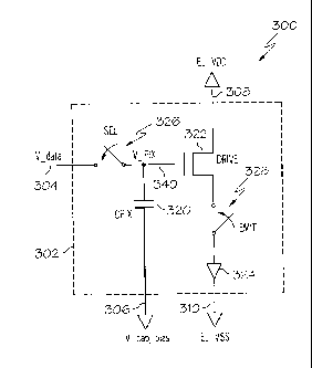
of the pixels of the
first row of the pixel array 202. In the illustrated example, the V_data
signal level 524 represents
the programmed voltage on one data line driving pixels in the display. With
reference to FIG. 2,
the V_data signal level 524 corresponds to the voltage present on one data
line that is connected
to all pixels in a particular row of the pixel array 202. The voltage depicted
by the V_data signal
level 524 is programmed into a voltage storage device, such as the CPIX
capacitor 320, of a
pixel in the row with an asserted select line, such as a line conveying the
SEL1 control line
signal level 520.
[0063] The display brightness reduction signal diagram 500 depicts several
time intervals that
are similar to the time intervals described above with regards to FIG. 4. A
first row
programming time interval 506 is shown during which the SEL1 control line
signal level 520 is
in a high stat 542, and the V_data signal level 524 is in a first pixel row
data level 550. The
EMIT control signal level 522 is in a low, or un-asserted, state during the
first row programming
time interval 506, indicating that pixels are not emitting light during this
interval.
- 24 -
CA 02824661 2013-08-23
= [0064] A sequence of other rows programming time intervals 508 is shown
to follow the first
row programming time interval 506. In the other rows programming time
intervals 508, the
V_data signal line 524 is set to voltage levels corresponding to the intensity
of the corresponding
pixel in a particular row and the SEL line (not shown) for that row is
asserted to indicate that the
pixel is to be programmed with that intensity level. During the other rows
programming time
intervals 508, the EMIT control signal is low, or un-asserted, indicating that
the pixels are not to
emit light during this time interval. The V_cap_bias signal level 526 is also
at a low level during
the other rows programming time intervals to cause the respective CPIX
capacitors of the pixels
in these rows to be programmed with, by being charged to, the programmed
voltage present on
the respective V_data lines during these time intervals. It is noted that the
programming of
pixels during the first program row programming time interval and the other
rows programming
time intervals 508 in one example is similar to the programing of active
matrix pixels in
conventional active matrix display structures with the exception of the
presence of the
V_cap_bias signal level 526.
[0065] In the display brightness reduction signal diagram 500, an emission
time interval 516
follows the above described pixel programming time intervals. During the
emission time
interval 516, the SEL lines, which are similar to the row scan lines 250, 252,
and 254 described
above with regards to FIG. 2, are in a low states, or un-asserted. The
voltages present on the
V_data lines, such as the depicted V_data line level 524, therefore do not
affect pixel operation
since the SEL lines are low and the SEL switches 326 in the pixels are open.
As illustrated in the
display brightness reduction signal diagram 500, the emission time interval
516 follows a period
during which all pixels are programmed with their programmed intensity values.
As illustrated,
the emission time interval 516 follows the first row programming time interval
506 and the other
- 25 -
CA 02824661 2013-08-23
rows programming time intervals 508. This is in contrast to some conventional
displays where
the pixels of each row are programmed with their programmed intensity levels
and then
configured to emit light at their programmed intensity level while pixels of
another row are
programmed with their programmed intensity values.
[0066] The EMIT control signal level 522 is in a high, or asserted, state
during the emission
time interval 516. With reference to FIG. 3, the high level of the EMIT
control signal level 522
causes the EMIT switch 328 to close, and completes the circuit from EL_VDD
power line 308 to
EL VS S power line 310 through the drive transistor 322 and the OLED element
324. As
discussed above, the electrical current flowing through the drive transistor
322, and therefore
through the OLED element 324, is controlled by the voltage between the gate
and source of the
drive transistor 322. As discussed below, the voltage between the gate of the
drive transistor
322, which is connected to the V_PIX line 340, and the source of the drive
transistor 322, which
is connected to EL VS S 310 via the OLED element 324, is increased by stepping
up the voltage
on the V_cap_bias line 306 during time sub-intervals of the emission time
interval 516.
[0067] The emission time interval 516 is shown to be divided into four time
sub-intervals, a first
emission time sub-interval 570, a second emission time sub-interval 572, a
third emission time
sub-interval 574, and a fourth emission time sub-interval 576. The display
brightness reduction
signal diagram 500 depicts the stepped increase of levels of the V_cap_bias
signal level during
the emission time interval 516. In this example, the V_cap_bias signal level
is shown to be a
first bias level 560 during the first emission time sub-interval 570, a second
bias level 562 during
the second emission time sub-interval 572, a third bias level 564 during the
third emission time
sub-interval 574, and a fourth bias level 566 during the fourth emission time
sub-interval 576.
- 26 -
CA 02824661 2013-08-23
[0068] As illustrated in the display brightness reduction signal diagram 500,
the voltage of the
V_cap_bias signal level is increased by AV1 during the first emission time sub-
interval 570, by
AV2 during the second emission time sub-interval 572, by AV3 during the third
emission time
sub-interval 574, and by AV4 during the fourth emission time sub-interval 576.
As shown in
FIG. 3, an increase in the voltage level on the V_cap_bias line 306 causes an
increase in the
voltage present on the V_PIX line 340, which is the gate voltage of the drive
transistor 322.
[0069] FIG. 6 illustrates a brightness reduction emission comparison diagram
600, according to
one example. The brightness reduction emission comparison diagram 600 depicts
the brightness
of light emitted by two pixels of an Active Matrix Organic Light Emitting
Diode (AMOLED)
display that incorporates an example display brightness reduction. The display
brightness
reduction implemented in this example is based upon a ramp of the voltage on
the V_cap_bias
line as is discussed above. The brightness reduction emission comparison
diagram 600 depicts
the values of signals present in the AMOLED display pixel circuit diagram 300,
discussed above.
The following discussion refers to two pixels, a first pixel and a second
pixel. In one example,
each of these two pixels has a design similar to that described with regards
to the AMOLED
display pixel circuit diagram 300 and the following description refers to
elements described
therein.
[0070] The brightness reduction emission comparison diagram 600 includes three
primary time
intervals, a first pixel programming interval 606, a second pixel programming
interval 608, and
an emission time interval 516. The emission time interval 516 is similar to
the emission time
interval 516 described above with regards to the display brightness reduction
signal diagram of
FIG. 5. The emission time interval 516 is shown to be divided into four time
sub-intervals, a
- 27 -
CA 02824661 2013-08-23
,
first emission time sub-interval 570, a second emission time sub-
interval 572, a third emission
time sub-interval 574, and a fourth emission time sub-interval 576.
[0071] The brightness reduction emission comparison diagram 600 includes a
V_cap_bias signal
level 620. As is described above with regards to display brightness reduction
signal diagram
500, the V_cap_bias signal level 620 is at a low level during pixel
programming, such as during
the first pixel programing time interval 606 and the second pixel programming
time interval 608.
In the following discussion, this low level is referred to as a baseline
level. In one example, the
baseline level of the V_cap_bias level 620 is a ground voltage potential.
[0072] When operating to reduce the emitted brightness of the display, one
example increases
the voltage on the V_cap_bias line 306 during the emission time interval. In
one example, the
voltage of the V cap bias line 306 is increased in steps such that the voltage
on the V_cap_bias
line 306 is increased during each time sub-interval of the emission time
interval 516. As
represented by the V_cap_bias signal level 620, during the first emission time
sub-interval 570,
V_cap_bias is increased over a baseline voltage a AV1 to a first bias level
560, during a second
emission time sub-interval 572 V_cap_bias is increased to a second bias level
562 that is AV2
above the baseline voltage, during a third emission time sub-interval 574
V_cap_bias is
increased to a third bias level 564 that is AV3 above the baseline voltage,
and during a fourth
emission time sub-interval 576 V_cap_bias is increased to a second bias level
566 that is A V4
above the baseline voltage. In further examples, the brightness of the display
is able to be
reduced by increasing the voltage of the V_cap_bias line 306 in any suitable
manner. It is to be
noted that a display is able to be operated at full intensity by not
increasing the voltage on the
V_cap_bias line 306, thereby keeping the voltage of the V_cap_bias line 306 at
the baseline
voltage.
- 28 -
CA 02824661 2013-08-23
, [0073] The brightness reduction emission comparison diagram 600 also
depicts a V_datal level
624 and a V data2 level 632. The V datal level 624 and the V data2 level 632
indicate the
_ _ _
emission intensity, which corresponds to a brightness or luminance value for
the pixel, that the
pixel is to emit during the emission time interval. The V_datal level 624
indicates a first pixel
intensity value 640, which corresponds to the intensity value that is
programmed into the first
pixel during that pixel's programming time interval. The V_data2 signal level
632 indicates a
second pixel intensity value 680, which is the intensity value that is
programmed into the second
pixel during that pixel's programming time interval.
[0074] With reference to FIG. 3, the first pixel intensity value 640 and the
second pixel intensity
value 680 correspond to voltages of the V_data line 304 during the time that
the SEL switch 326
is closed for the first pixel and the second pixel, respectively. As discussed
above, the drive
transistor 322 in the illustrated example is a P-Channel FET transistor. As
such, higher intensity
levels are programmed into the pixel by placing a lower voltage on the V PIX
line. An
intensity, or brightness, level of a pixel is programmed into the pixel by the
operation of the SEL
switch 326, which causes an intensity programming voltage to be charged onto
the CPIX
capacitor 320 of a pixel being programmed. After that CPIX capacitor is
charged, the SEL
switch 326 opens and, due to the high impedance of the gate of the drive
transistor 322, the CPIX
capacitor 320 retains the voltage to which it was charged. The SEL switch 326
in one example is
operated based upon logic levels of row scan lines for the display, as is
described above.
[0075] The first pixel intensity value 640 and the second pixel intensity
value 680 are shown to
occur at different time intervals in order to more clearly describe certain
aspects of this example.
It is clear that these two data voltages are able to be programmed into these
respective pixels in
the same row by using with different data lines. It is also clear that these
two pixels are able to
- 29 -
CA 02824661 2013-08-23
,
be in the same column of the display, and therefore programmed by data
voltages carried on the
same data line, but at different times that are indicated by the logic levels
of associated row scan
lines.
[0076] The example illustrated by the brightness reduction emission comparison
diagram 600
depicts the first pixel intensity value 640 to be higher than the second pixel
intensity value 680.
Due to the structure of the active circuits in this example pixel, the higher
intensity level of the
first pixel intensity value 640 result in a lower voltage being charged onto
the CPIX capacitor
326 of the first pixel than is charged onto the CPIX capacitor 326 of the
second pixel. Stating
the converse, the CPIX capacitor 326 of the second pixel is charged with a
higher voltage than
the CPIX capacitor 326 of the first pixel in this example.
[0077] The brightness reduction emission comparison diagram 600 depicts two
luminance level
traces, a first luminance level trace 630 and a second luminance level trace
634. The first
luminance level trace 630 indicates the luminance, or light emission
intensity, of the first pixel,
and the second luminance level trace 634 indicates the luminance, or light
emission intensity, of
the second pixel. The luminance of an OLED element is known to be
proportionate to the
amount of electrical current passing through the OLED element. The luminance
level traces
therefore are representative of the electrical current flowing through their
respective OLED
elements. With reference to FIG. 3, the electrical current that flows through
the OLED element
324 of a pixel with the design portrayed in FIG. 3 is controlled by the
voltage difference between
the gate and source of the drive transistor 322, which is the voltage
difference between the
V PIX line 340 and EL _VSS 310 less the voltage drop across the OLED element
324.
_
- 30 -
CA 02824661 2013-08-23
.
[0078] It is noted that the first luminance level trace 630 and the
second luminance level trace
634 have a low, or zero, level 610, 612 during the programming time intervals,
such as the first
pixel programming time interval 606 and the second pixel programming time
interval 608. This
is due to the operation of the EMIT switch 328, which is open in this example,
and not
conducting, during the programming time intervals.
[0079] During the emission time interval 516, the first luminance trace level
630 depicts the
luminance level emitted by, which is proportional to the electrical current
flowing through, the
first pixel. The first pixel is programmed to emit an intensity level that is
set by the first pixel
intensity value 640 by programming a first intensity voltage onto the CPIX
capacitor 326 of the
first pixel. The luminance, or emitted light intensity, of the first pixel is
based upon the voltage
difference between the V _PIX line 340 of the first pixel and the voltage of
the source of the drive
transistor 322 - EL _VSS 310 less the voltage across the OLED element 324,
which controls the
electrical current passing through the drive transistor 322 of that pixel. The
voltage of the
V _PIX line 340 of a particular pixel is the respective sum of the voltage
across the CPIX
capacitor 320 and the voltage of the V_cap_bias line 306 for that pixel. The
ramping up of the
voltage of the V_cap_bias line 340 during the emission time interval 516
causes the voltage of
the V PIX line 340 to correspondingly increase, and thereby decreases the
electrical current
flowing through the P-Channel FET drive transistor 322 and the OLED element
324. In the
following discussion, the voltage on the V_PIX line 340 is referred to as
Vgate because this is the
voltage on the gate of the drive transistor 322. It is clear that Vgate is the
sum of the voltage
charged across the CPIX capacitor 320 and the voltage on the V_cap_bias line
306, which is
illustrated as an increasing step function during the emission time interval
516.
- 31 -
CA 02824661 2013-08-23
.
[0080] During the illustrated first emission time sub-interval 570, the
first luminance trace level
indicates the first pixel emits light with a first pixel first luminance level
642. The first pixel first
luminance level 642 is based upon the difference between Vgate and the voltage
of the gate of the
drive transistor 322, which is EL _VSS 310 less the voltage across the OLED
element 324.
During the first emission time sub-interval 570, Vgate, which is the sum of
V_cap_bias and the
voltage on the CPIX capacitor, is increased by a value of V_EM1, which is the
increase in the
voltage of V_cap_bias over the baseline voltage. The increase of Vgate reduces
the electrical
current flowing through the OLED element 324 of the first pixel and
correspondingly reduces the
emitted intensity of the pixel during the first emission time sub-interval by
a corresponding
amount.
[0081] During the second emission time sub-interval 572, the first luminance
trace level
indicates the first pixel emits light with a first pixel second luminance
level 644. During the
second emission time sub-interval 572, Vgate is increased by a value of V_EM2
above the
baseline V_cap_bias voltage. In this example, V_EM2 is larger than the voltage
increase of the
previous sub-interval, i.e., V_EM1, and therefore Vgate is further increased
during the second
emission time sub-interval 572 relative to the first emission time sub-
interval 570. Due to the
further increase in Vgate, the electrical current flowing through the OLED
element 324 of the first
pixel, and the corresponding emitted intensity of the pixel during the second
emission time sub-
interval 572, are further reduced during the second emission time sub-interval
572 relative to the
first emission time sub-interval 570.
[0082] During the third emission time sub-interval 574, the first luminance
trace level indicates
the first pixel emits light with a third pixel first luminance level 646. The
first pixel third
luminance level 646 is lower than the first pixel second luminance level 644
because Vgate is
- 32 -
CA 02824661 2013-08-23
= increased by a value of V_EM3 above the baseline value, which is greater
than the value of
V EM2. This greater increase in Vgate causes an even greater reduction in
electrical current
flowing through the OLED element 324 of the first pixel and a correspondingly
greater reduction
of the emitted intensity of the pixel during the third emission time sub-
interval by a
corresponding amount.
[0083] During the fourth emission time sub-interval 576, the first luminance
trace level indicates
the first pixel emits light with a first pixel fourth luminance level 648. The
first pixel fourth
luminance level 648 is lower than the first pixel third luminance level 646
because Vgate is
increased by a value of V_EM4 above the baseline value, which is greater than
the value of
V EM3. In the illustrated example, the value of V EM4 is sufficiently large
that the first pixel
_ _
fourth luminance level 648 is reduced to a level near zero. In other words, in
this illustrated
example, the OLED element 324 is not emitting light during the fourth emission
time sub-
interval 576.
[0084] With regards to the second pixel, the second luminance trace level 634
indicates that the
second pixel emits light with a second pixel first luminance level 682 during
the first emission
time sub-interval 570. The second pixel first luminance level 682 is based
upon the difference
between Vgate and the source of the drive transistor 322, which is EL _VSS 310
less the voltage
across the OLED element 324. Because the second pixel intensity value 680 is
lower than the
first pixel intensity value 640, the CPIX capacitor 320 of the second pixel in
this example is
charged to a higher voltage than the CPIX capacitor 320 of the first pixel.
This results in a
higher value of Vgate, for this second pixel during the first emission time
sub-interval 570. As
described above with regards to the first pixel, the value of Vgate is
increased in this example
during the first emission time sub-interval 570 by a value of V_EM1, which is
the increase in the
- 33 -
CA 02824661 2013-08-23
.
voltage of V cap bias over the baseline voltage. The increase of Vgate
reduces the electrical
current flowing through the OLED element 324 of the first pixel and
correspondingly reduces the
emitted intensity of the pixel during the first emission time sub-interval by
a corresponding
amount.
[0085] During the second emission time sub-interval 572, the second luminance
trace level 634
indicates that the second pixel emits light with a second pixel second
luminance level 684.
During the second emission time sub-interval 572, Vgate is increased by a
value of V_EM2 above
the baseline V_cap_bias voltage. In this example, V_EM2 is larger than the
voltage increase of
the previous sub-interval, i.e., V_EM1, and therefore Vgate is further
increased during the second
emission time sub-interval 572 relative to the first emission time sub-
interval 570. Due to the
further increase in Vgate, the electrical current flowing through the OLED
element 324 of the
second pixel, and the corresponding emitted intensity of the pixel during the
second emission
time sub-interval 572, are further reduced during the second emission time sub-
interval 572
relative to the first emission time sub-interval 570. Due to the lower
programmed intensity level
for the second pixel, it is noted that the second pixel second luminance level
684 is near the zero
level in this example. The increase in the voltage on the V_cap_bias line 306
to V_EM2 caused
Vgate, to increase to a level that essentially halted
[0086] FIG. 7 illustrates a pixel intensity command vs. emitted intensity
chart 700, according to
one example. The pixel intensity command vs. emitted intensity chart 700
includes an intensity
command, or grayscale value, axis 702 and an emitted intensity axis 704. The
intensity
command axis 702 represents the intensity, or brightness, value that is
programmed into the
pixel. The brightness of the pixel is also referred to as a grayscale value
for that pixel. Referring
to FIG. 3, the intensity command provided to a pixel is represented by the
voltage on the V_data
- 34 -
CA 02824661 2013-08-23
-
line 304, and operates to control the electrical current that flows
though the OLED element 324
of that pixel during the emission time interval. The emitted intensity axis
704 indicates the
intensity of light emitted by the OLED element of the pixel. The intensity of
light emitted by an
OLED element is proportional to the electrical current flowing through the
OLED element.
[0087] The pixel intensity command vs. emitted intensity chart 700 depicts two
gamma curves, a
full brightness gamma curve 706 and a reduced brightness gamma curve 708. The
full
brightness gamma curve 706 and the reduced brightness gamma curve 708 indicate
relationships
between intensity commands provided to a pixel, as indicated by values along
the intensity
command axis 702, and the emitted light intensity produced by the OLED element
of the pixel.
[0088] The full brightness gamma curve 706 indicates this relationship for a
pixel that is not
performing the above described brightness reduction processing. Referring to
the example
presented in FIG. 3, the full brightness gamma curve 706 reflects the pixel
intensity command to
emitted intensity when the V_cap_bias line 306 is held at a baseline voltage,
which is usually a
low or zero voltage, during the emission time interval.
[0089] The reduced brightness gamma curve 708 indicates this relationship for
a pixel that is
performing the above described brightness reduction processing. Referring to
the example
presented in FIGs. 3 and 6, the reduced brightness gamma curve 708 reflects
the pixel intensity
command to emitted intensity when the V_cap_bias line 306 has a voltage that
is above the
baseline voltage during the emission time interval.
[0090] The two gamma curves depicted in the pixel intensity command vs.
emitted intensity
chart 700 illustrate the difference in emitted light intensity between a pixel
that is not performing
brightness reduction and a pixel that is performing brightness reduction. This
difference is
- 35 -
CA 02824661 2013-08-23
-
shown for two intensity command values, a datal value 710 and a data2
value 712. In this
example, the datal value 710 is a higher value, i.e., it indicates a brighter
intensity for the pixel,
than the data2 value 712. Due to the non-linear response of these gamma
curves, the command
for brighter intensity, the datal value 710 in this example, results in a
greater decrease in emitted
light brightness between the pixel that is not performing brightness reduction
and the pixel that is
performing brightness reduction, than the reduction in brightness for the
data2 value 712.
[0091] The datal value 710 is shown to intersect the full brightness gamma
curve 706 at a first
high brightness point 740. The first high brightness point 740 indicates an
emitted intensity
value of IIH 720. The datal value 710 is shown to intersect the reduced
brightness gamma curve
708 at a first low brightness point 742. The first low brightness point 742
indicates an emitted
intensity value of II L 722. The difference between Im 720 and IH, 722 is
shown to be Aintensityi
730.
[0092] The data2 value 712 is shown to intersect the full brightness gamma
curve 706 at a
second high brightness point 744. The second high brightness point 744
indicates an emitted
intensity value of I2H 724. The data2 value 712 is shown to intersect the
reduced brightness
gamma curve 708 at a second low brightness point 746. The second low
brightness point 746
indicates an emitted intensity value of In 726. The difference between 12H 724
and I2L 726 is
shown to be Aintensity2 732.
[0093] The full brightness gamma curve 706 and the reduced brightness gamma
curve 708 are
noted to have a similar shape with a monotonically increasing slope with
increasing values of
intensity commands. This increasing slope of the gamma curves results in the
value of
Aintensityi 730 being greater than Aintensity2 732. Due to this relationship,
pixels that are
- 36 -
CA 02824661 2013-08-23
= programmed to emit brighter intensities have a greater reduction of
emitted light intensity when
performing the above described brightness reduction processing. This reduction
of emitted light
intensity in proportion to the brightness command for the pixel implements an
automatic gamma
reduction in the display. The above described example further implements this
selective and
display wide gamma reduction by adding a single signal path, the V_cap bias
line 306, to the
display and without adding components to each pixel of the display. Further,
the above
described examples provide a computationally efficient technique to provide a
proportional
brightness reduction based on programmed pixel intensity in that the above
described example
does not perform pixel-by-pixel image processing to apply a proportional
brightness reduction to
each brightness command in the data defining each image to be displayed.
[0094] FIG. 8 illustrates a display brightness reduction processing flow 800,
according to one
example. The display brightness reduction processing flow 800 is performed in
one example by
circuits that drive the pixels of a display, such as are described above with
regards to the
AMOLED display component diagram 200 with regards to FIG. 2, operating in
conjunction with
pixels similar to the AMOLED display pixel circuit diagram 300 described with
regards to FIG.
3. The following description refers to elements of FIGs. 2 and 3.
[0095] The display brightness reduction processing flow 800 begins by
receiving, at 802, an
image to display. In one example, an image to be displayed is generated by a
processor creating,
for example, a user interface display. In further examples, images are
retrieved from a storage to
be displayed as an image or as part of a motion picture. Further examples of
images are also able
to be received. In one example, the image to be displayed is received by an
image source 204
and is provided to the scan generator 230 and the data generator 232.
-37 -
CA 02824661 2013-08-23
= [0096] The display brightness reduction processing flow 800 continues by
programming, at 804,
a respective programmed voltage into each pixel. In one example, the
respective program
voltage represents a brightness to be emitted by the respective pixel being
programmed. This
brightness value is determined, in one example, based upon the image data
received in the above
step. In the example described above, this programming is performed by
charging the CPIX
capacitor 320 with the programmed voltage that is delivered on the V_data line
304. As
described above, the programming of voltages indicating emitted light
intensity for a pixel is
performed on each pixel of the pixel array 202 by the operation of the scan
generator 230 and the
data generator 232.
[0097] The display brightness reduction processing flow 800 continues by
generating, at 806, an
intensity reduction input voltage during the emission time duration of the
display. In one
example, the intensity reduction input voltage has a time varying waveform,
such as the stepped
ramp function described above. In one example, a controller is able to not
perform emitted
intensity reduction processing by generating an intensity reduction input
voltage that is at a
baseline level, such as at a ground voltage, for the duration of the emission
time duration.
[0098] The display brightness reduction processing flow 800 continues by
receiving, at 808, the
intensity reduction input voltage at each pixel within the display. In one
example, the intensity
reduction input voltage is received along a conductive coupling that is
coupled to each pixel
within the display.
[0099] The display brightness reduction processing flow 800 continues by
controlling, at 810,
electrical current driving a light emitting element of each pixel in the
display based upon a sum
of the respective programmed voltage programmed into the respective pixel and
the intensity
-38-
CA 02824661 2013-08-23
= reduction voltage. In one example, the electrical current is controlled
in each pixel by coupling a
gate of a thin film transistor fabricated adjacent to the light emitting
element to a series
combination of a voltage storage device charged with the programmed voltage
and the intensity
reduction input voltage.
[00100] The display brightness reduction processing flow 800
proceeds by determining, at
812, if the emission time duration has ended. If the emission time duration
has not ended, the
display brightness reduction processing flow 800 returns to generating, at
806, the intensity
reduction input voltage, as described above. If the emission time duration has
ended, the display
brightness reduction processing flow 800 returns to receiving, at 802, an
image, as is described
above.
[00101] FIG. 9 is a block diagram of an electronic device and
associated components 900
in which the systems and methods disclosed herein may be implemented. In this
example, an
electronic device 952 is a wireless two-way communication device with voice
and data
communication capabilities. Such electronic devices communicate with a
wireless voice or data
network 950 using a suitable wireless communications protocol. Wireless voice
communications
are performed using either an analog or digital wireless communication
channel. Data
communications allow the electronic device 952 to communicate with other
computer systems
via the Internet. Examples of electronic devices that are able to incorporate
the above described
systems and methods include, for example, a data messaging device, a two-way
pager, a cellular
telephone with data messaging capabilities, a wireless Internet appliance or a
data
communication device that may or may not include telephony capabilities. A
particular example
of such an electronic device is the handheld communications device 100,
discussed above.
-39-
CA 02824661 2013-08-23
[00102]
The illustrated electronic device 952 is an example electronic device
that includes
=
two-way wireless communications functions.
Such electronic devices incorporate
communication subsystem elements such as a wireless transmitter 910, a
wireless receiver 912,
and associated components such as one or more antenna elements 914 and 916. A
digital signal
processor (DSP) 908 performs processing to extract data from received wireless
signals and to
generate signals to be transmitted. The particular design of the communication
subsystem is
dependent upon the communication network and associated wireless
communications protocols
with which the device is intended to operate.
[00103]
The electronic device 952 includes a microprocessor 902 that controls
the overall
operation of the electronic device 952. The microprocessor 902 interacts with
the above
described communications subsystem elements and also interacts with other
device subsystems
such as flash memory 906, random access memory (RAM) 904. The flash memory 906
and
RAM 904 in one example contain program memory and data memory, respectively.
The
microprocessor 902 also interacts with an auxiliary input/output (I/0) device
938, a USB Port
928, a display 934, a keyboard 936, a speaker 932, a microphone 930, a short-
range
communications subsystem 920, a power subsystem 922, and any other device
subsystems.
[00104]
The electronic device 952 is an example of an electronic display device,
which
includes a display 934. The display 934 in various examples is an AMOLED based
display such
as is described above with regards to FIG. 2. In various examples, the
microprocessor 902
determines an amount of brightness reduction to be applied to the display 934
and provides a
brightness reduction level input to the display 934, or associated circuitry
of other examples, in
order to implement the above described reduction of pixel emitted intensity.
In various
examples, the amount of brightness reduction is determined by a user input, a
detection of a level
- 40 -
CA 02824661 2013-08-23
= of ambient light, other criteria, or combinations of these factors. The
microprocessor 902 in one
example is further able to provide data to the display 934 that defines images
or other
,
presentations to display to, for example, a user of the electronic device 952.
[00105] A battery 924 is connected to a power subsystem 922 to
provide power to the
circuits of the electronic device 952. The power subsystem 922 includes power
distribution
circuitry for providing power to the electronic device 952 and also contains
battery charging
circuitry to manage recharging the battery 924. The power subsystem 922
includes a battery
monitoring circuit that is operable to provide a status of one or more battery
status indicators,
such as remaining capacity, temperature, voltage, electrical current
consumption, and the like, to
various components of the electronic device 952.
[00106] The USB port 928 further provides data communication
between the electronic
device 952 and one or more external devices. Data communication through USB
port 928
enables a user to set preferences through the external device or through a
software application
and extends the capabilities of the device by enabling information or software
exchange through
direct connections between the electronic device 952 and external data sources
rather then via a
wireless data communication network.
[00107] Program information, which is able to include machine
readable program code
that defines various operating programs including operating system software,
application
programs, and the like, that is used by the microprocessor 902 is stored in
flash memory 906.
Further examples are able to use a battery backed-up RAM or other non-volatile
storage data
elements to store program information such as operating systems, other
executable programs, or
both. The operating system software, device application software, or parts
thereof, are able to be
- 41 -
CA 02824661 2013-08-23
- temporarily loaded into volatile data storage such as RAM 904. Data
received via wireless
communication signals or through wired communications are also able to be
stored to RAM 904.
[00108] The microprocessor 902, in addition to its operating system
functions, is able to
execute software applications on the electronic device 952. A predetermined
set of applications
that control basic device operations, including at least data and voice
communication
applications, is able to be installed on the electronic device 952 during
manufacture. Examples
of applications that are able to be loaded onto the device may be a personal
information manager
(PIM) application having the ability to organize and manage data items
relating to the device
user, such as, but not limited to, e-mail, calendar events, voice mails,
appointments, and task
items. Further applications include applications that have input cells that
receive data from a
user.
[00109] Further applications may also be loaded onto the electronic
device 952 through,
for example, the wireless network 950, an auxiliary I/O device 938, USB port
928, short-range
communications subsystem 920, or any combination of these interfaces. Such
applications are
then able to be installed by a user in the RAM 904 or a non-volatile store for
execution by the
microprocessor 902.
[00110] In a data communication mode, a received signal such as a
text message or web
page download is processed by the communication subsystem, including wireless
receiver 912
and wireless transmitter 910, and communicated data is provided the
microprocessor 902, which
is able to further process the received data for output to the display 934, or
alternatively, to an
auxiliary I/O device 938 or the USB port 928. A user of the electronic device
952 may also
compose data items, such as e-mail messages, using the keyboard 936, which is
able to include a
- 42 -
CA 02824661 2013-08-23
= complete alphanumeric keyboard or a telephone-type keypad, in conjunction
with the display
934 and possibly an auxiliary I/O device 938. Such composed items are then
able to be
transmitted over a communication network through the communication subsystem.
[00111] For voice communications, overall operation of the
electronic device 952 is
substantially similar, except that received signals are generally provided to
a speaker 932 and
signals for transmission are generally produced by a microphone 930.
Alternative voice or audio
I/O subsystems, such as a voice message recording subsystem, may also be
implemented on the
electronic device 952. Although voice or audio signal output is generally
accomplished
primarily through the speaker 932, the display 934 may also be used to provide
an indication of
the identity of a calling party, the duration of a voice call, or other voice
call related information,
for example.
[00112] Depending on conditions or statuses of the electronic
device 952, one or more
particular functions associated with a subsystem circuit may be disabled, or
an entire subsystem
circuit may be disabled. For example, if the battery temperature is low, then
voice functions may
be disabled, but data communications, such as e-mail, may still be enabled
over the
communication subsystem.
[00113] A short-range communications subsystem 920 is a further
optional component
which may provide for communication between the electronic device 952 and
different systems
or devices, which need not necessarily be similar devices. For example, the
short-range
communications subsystem 920 may include an infrared device and associated
circuits and
components or a Radio Frequency based communication module such as one
supporting
- 43 -
CA 02824661 2013-08-23
Bluetooth communications, to provide for communication with similarly-enabled
systems and
devices.
[00114] A media reader 960 is able to be connected to an auxiliary I/O
device 938 to
allow, for example, loading computer readable program code of a computer
program product
into the electronic device 952 for storage into flash memory 906. One example
of a media reader
960 is an optical drive such as a CD/DVD drive, which may be used to store
data to and read
data from a computer readable medium or storage product such as computer
readable storage
media 962. Examples of suitable computer readable storage media include
optical storage media
such as a CD or DVD, magnetic media, or any other suitable data storage
device. Media reader
960 is alternatively able to be connected to the electronic device through the
USB port 928 or
computer readable program code is alternatively able to be provided to the
electronic device 952
through the wireless network 950.
[00115] Information Processing System
[00116] The present subject matter can be realized in hardware, software,
or a
combination of hardware and software. A system can be realized in a
centralized fashion in one
computer system, or in a distributed fashion where different elements are
spread across several
interconnected computer systems. Any kind of computer system - or other
apparatus adapted for
carrying out the methods described herein - is suitable. A typical combination
of hardware and
software could be a general purpose computer system with a computer program
that, when being
loaded and executed, controls the computer system such that it carries out the
methods described
herein.
- 44 -
CA 02824661 2013-08-23
[00117] The present subject matter can also be embedded in a computer
program product,
which comprises all the features enabling the implementation of the methods
described herein,
and which - when loaded in a computer system - is able to carry out these
methods. Computer
program in the present context means any expression, in any language, code or
notation, of a set
of instructions intended to cause a system having an information processing
capability to
perform a particular function either directly or after either or both of the
following a) conversion
to another language, code or, notation; and b) reproduction in a different
material form.
[00118] Each computer system may include, inter alia, one or more
computers and at least
a computer readable medium allowing a computer to read data, instructions,
messages or
message packets, and other computer readable information from the computer
readable medium.
The computer readable medium may include computer readable storage medium
embodying
non-volatile memory, such as read-only memory (ROM), flash memory, disk drive
memory, CD-
ROM, and other permanent storage. Additionally, a computer medium may include
volatile
storage such as RAM, buffers, cache memory, and network circuits. Furthermore,
the computer
readable medium may comprise computer readable information in a transitory
state medium such
as a network link and/or a network interface, including a wired network or a
wireless network,
that allow a computer to read such computer readable information.
[00119] As required, detailed embodiments are disclosed herein; however,
it is to be
understood that the disclosed embodiments are merely examples and that the
systems and
methods described below can be embodied in various forms. Therefore, specific
structural and
functional details disclosed herein are not to be interpreted as limiting, but
merely as a basis for
the claims and as a representative basis for teaching one skilled in the art
to variously employ the
disclosed subject matter in virtually any appropriately detailed structure and
function. Further,
- 45 -
CA 02824661 2015-09-02
the terms and phrases used herein are not intended to be limiting, but rather,
to provide an
understandable description.
[00120] The terms "a" or "an", as used herein, are defined as one or more
than one. The
term plurality, as used herein, is defined as two or more than two. The term
another, as used
herein, is defined as at least a second or more. The terms "including" and
"having," as used
herein, are defined as comprising (i.e., open language). The term "coupled,"
as used herein, is
defined as "connected," although not necessarily directly, and not necessarily
mechanically. The
term "configured to" describes hardware, software or a combination of hardware
and software
that is adapted to, set up, arranged, built, composed, constructed, designed
or that has any
combination of these characteristics to carry out a given function. The term
"adapted to"
describes hardware, software or a combination of hardware and software that is
capable of, able
to accommodate, to make, or that is suitable to carry out a given function.
[00121] Although specific embodiments of the subject matter have been
disclosed, those
having ordinary skill in the art will understand that changes can be made to
the specific
embodiments without departing from the scope of the disclosed subject matter.
The scope of the
disclosure is not to be restricted, therefore, to the specific embodiments,
and it is intended that
the appended claims cover any and all such applications, modifications, and
embodiments within
the scope of the present disclosure.
- 46 -