Note: Descriptions are shown in the official language in which they were submitted.
CA 02824895 2013-07-16
WO 2012/097866 PCT/EP2011/050560
1
A high voltage dc power source and a power apparatus for a
high voltage electrical power system
TECHNICAL FIELD
The present invention relates to a high voltage dc power source for
providing a charging current to an electronic device. By a high voltage
dc power source should be understood dc power source units connected
in series to be within the range of 3 kV and upwards, preferably in the
range of 10 kV and upwards. The invention further relates to a power
apparatus for a high voltage electrical power system including a high
voltage dc power source connected in parallel. With a power apparatus
is meant an apparatus that is capable of controlling reactive power
and/or active power. Examples of power apparatus are a power
compensator and an uninterruptible power supply (UPS). High voltage
electrical power systems can be networks for transmission or
distribution of electrical energy as well as industries, hospitals and such.
BACKGROUND OF THE INVENTION
Within flexible alternating current transmission systems (FACTS) a
plurality of control apparatus are known. One such FACTS apparatus is
a static compensator (STATCOM). A STATCOM comprises a voltage
source converter (VSC) having an AC side connected to a high voltage
electrical power system and a DC side connected to a temporary electric
power storage means such as capacitors. The STATCOM can supply
reactive power to or absorb reactive power from the transmission line.
As opposed to the STATCOM, which only compensates for reactive
power, another concept is to connect a dc power source to a STATCOM,
and thus being able to perform active power compensation. Such a
CA 02824895 2013-07-16
WO 2012/097866 PCT/EP2011/050560
2
power apparatus may be used e.g. as a spinning reserve and for
compensating for fluctuating energy levels in the power system.
Today the dc power source is a high voltage battery. Since the power
apparatus is connected to the ac voltage of the high voltage electrical
power system, a large number of battery cells have to be connected in
series to match the dc voltage of the power apparatus. Moreover, to
obtain a desired amount of electric energy (duration of active power) of
the energy storage, a number of strings including a plurality of battery
cells could be connected in parallel.
In WO/2009/152849 such a power apparatus comprising a voltage
source converter and a high voltage dc power source is presented. The
power apparatus further comprises solid-state switches which are
distributed among the dc power-source units of the string and
configured to disconnect the string in case of a fault. By providing each
of the dc power source units along the string with a solid-state switch
and turning the switches on and off simultaneously, each switch only
has to withstand the voltage over its corresponding dc power source
unit when the string is disconnected.
Restoring power after a wide-area power outage is a difficult task. A
plurality of power stations needs to be brought back on-line. Normally,
this is done with the help of power from the rest of the grid. In the
absence of grid power, a so-called black start needs to be performed to
boot strap the power grid into operation. To provide a black start, some
power stations are typically equipped with small diesel generators which
can be used to start larger generators, which in turn can be used to
start the main power station generators. Generating plants using steam
turbines require station service power of up to 10% of their capacity for
boiler feedwater pumps, boiler forced-draft combustion air blowers, and
for fuel preparation. It is, however, uneconomic to provide such a large
CA 02824895 2013-07-16
WO 2012/097866 PCT/EP2011/050560
3
standby capacity at each station, so black-start power must be provided
over the electrical transmission network from other stations.
An advantage with the power apparatus comprising battery energy
storage systems as described above is their ability to provide power to
the grid to which it is connected in case of a wide-area power outage
making it possible to provide a black start of the grid. In
WO/2008/002223 a power compensator is disclosed comprising a
voltage source converter, a dc link capacitor and an energy storage
device further comprising a high voltage battery, a first and second
main switch for disconnecting the battery from the capacitor. One of the
switches disconnects the string from the positive dc rail of the converter
and the other switch disconnects the string from the negative dc rail of
the converter. Each of the switches has to be rated for the entire
converter voltage to be capable of protecting the power apparatus. In
parallel with the main switches there are arranged a first and a second
parallel path containing a resistor means and a secondary switch. The
power compensator also comprises a control means for controlling the
switches. Further, a method for providing a black start of a dead
network is proposed. The method comprises the method steps of:
- energizing the dc link capacitor from the energy storage device;
- start switching the voltage source converter; and
- controlling the power flow of the power compensator to and from the
network in dependence on the balance of power producers and power
consumers connected to the network.
However, connecting the energy storage directly to the dc link capacitor
would lead to a large inrush current that might result in mechanical or
electrical damage to the battery energy storage system and/or
converter. It might also lead to a triggering of a short circuit detection
system of the power apparatus and consequently a shut down order of
the power apparatus. In the method disclosed in WO/2008/002223 and
CA 02824895 2015-05-22
4
described above this problem is solved by forming a current path
containing resistor means in order to decrease the current flow between
the dc link capacitor and the energy storage device. However, the
resistors are expensive, space requiring, non-controllable and run the
risk of becoming overheated.
SUMMARY OF THE INVENTION
It is an object of the invention to overcome or at least alleviate the
above-mentioned problem with large inrush currents. In particular, it is
an object of the invention to provide an improved high voltage dc power
source which reduces the large inrush current in a way that is more
controllable, less expensive and less space requiring.
According to one aspect, the invention provides a high voltage dc power
source for providing a charging current to an electronic device,
comprising:
one or more strings connected in parallel, each string being
subdivided into a plurality of dc power source units connected in series
and each string being provided with at least one solid-state switch
configured to connect and disconnect said string; and
a control unit adapted to turn on and turn off the at least one
solid-state switch;
wherein the control unit is configured, upon receiving an order to
connect the string, to control the at least one switch of the string to be
alternately turned on and off so that a soft charging of the electronic
device is achieved.
According to another aspect of the invention, there is provided a high
voltage dc power source for providing a charging current to an
electronic device, comprising:
CA 02824895 2015-05-22
4a
one or more strings connected in parallel, each string being
subdivided into a plurality of dc power source units connected in series
and each string being provided with a plurality of solid-state switches
configured to connect and disconnect said string; and
a control unit adapted to turn on and turn off the a plurality of
solid-state switches,
wherein each switch is arranged to connect and disconnect one of
the dc power source units of the string, and wherein the control unit is
configured, upon receiving an order to connect the string, to
simultaneously control the solid-state switches of the string to be
alternately turned on and off so that a soft charging of the electronic
device is achieved.
The high voltage dc power source for providing a charging current to an
electronic device according to the invention is characterized in that a
control unit is configured, upon receiving an order to connect a string,
to control at least one switch of the string to be alternately turned on
and off so that a soft charging of the electronic device is achieved. For
example a Pulse Width Modulation (PWM) scheme could be used.
An advantage with the high voltage dc power source according to the
invention is that by controlling the at least one solid-state switch of the
string to be alternately turned on and off a soft and more controllable
charging of the electronic device is achieved. Additionally, no resistor
means are needed which provides a less expensive and less space
requiring dc power source. Furthermore, no secondary switches are
needed as the same current path is used for the charging current as
well as for the operating current owing to the fact that the at least one
CA 02824895 2013-07-16
WO 2012/097866 PCT/EP2011/050560
solid-state switch is used for connecting and disconnecting the string as
well as a means for controlling the inrush current.
With a dc power source unit is meant a plurality of small dc power
5 source members connected in series and/or parallel and capable of
providing dc power, such as a battery cell, a photovoltaic cell, a fuel
cell, or a super capacitor. Different types of dc power source members
could also be combined in the high voltage dc power source.
In an embodiment of the invention, each string is provided with a
plurality of solid-state switches configured to connect and disconnect
said string, each switch is arranged to connect and disconnect one of
the dc power source units of the string and the control unit is
configured to simultaneously control the solid-state switches of the
string to be alternately turned on and off so that a soft charging of the
electronic device is achieved. The use of a plurality of solid-state
switches as mentioned above is necessary at certain voltage levels of
the dc power source since there are no solid-state switches available on
the market with such voltage ratings. A further advantage is that the
plurality of solid-state switches implies a lower voltage across each
switch and accordingly smaller and less expensive switches having
lower voltage ratings can be used.
In an embodiment of the invention, the control unit is configured to
vary the time interval between the turn on and the turn off or the time
interval between the turn off and the turn on of the switch to limit the
charging current until a predetermined voltage value across said
electronic device is achieved. Advantageously, varying the time interval
between the turn on and the turn off or the time interval between the
turn off and the turn on of the switch makes it possible to arbitrarily
control the magnitude of the charging current to the electronic device.
CA 02824895 2013-07-16
WO 2012/097866 PCT/EP2011/050560
6
In an embodiment of the invention, the control unit is configured to
gradually increase the time interval between the turn on and the turn
off of the switch. For instance, when the voltage difference between the
charging string (or strings) and the electronic device decreases as the
electronic device is charged, the control unit is able to gradually
increase the time interval between the turn on and the turn off of the
switch, thereby advantageously accelerating the charging process of the
electronic device without exceeding a harmful level of the charging
current.
In an embodiment of the invention, the control unit is configured to
gradually decrease the time interval between the turn off and the turn
on of the switch.
In an embodiment of the invention, the control unit is adapted to
determine said time interval based on measured values of said charging
current. Measuring the charging current makes it possible to
automatically adapt the time interval between the turn on and the turn
off of the switch based on current values of the charging current,
thereby optimising the control of the charging current.
In an embodiment of the invention, the control unit is configured to
control the at least one switch according to a predefined switching
pattern. An advantage with a predefined switching pattern is that the
charging current does not have to be measured and consequently no
charging current sensors are needed.
In an embodiment of the invention, the dc power source has two or
more parallel strings and the control unit is configured to control the at
least one switch of the string having highest voltage to be alternately
turned on and off so that a soft charging of one of the other strings
having lower voltage is achieved. For different reasons the voltage
CA 02824895 2013-07-16
WO 2012/097866 PCT/EP2011/050560
7
across a string of dc power source units can differ in relation to another
string or strings. For example, in cases where the string has been
temporarily disconnected for replacement of dc power source units or
where the string includes batteries with a different State Of Charge
(SOC) value due to aging of some of the battery cells in the string. In
such cases it is an advantage to be able to control the charging current
from the string having the highest voltage level to the string having the
lowest voltage level.
In an embodiment, each dc power source unit provides dc voltage at 1-
10 kV, preferably between 2 and 5 kV or approximately 3 kV. The high
voltage dc power source can be dimensioned for voltages between 10
kV and 100 kV, or even more than 100 kV.
According to a second aspect of the invention this object is achieved by
a power apparatus for a high voltage electrical power system, the
power apparatus comprising a voltage source converter having a dc link
capacitor connected in parallel and a high voltage dc power source
according to any of the previously mentioned embodiments. The control
unit of the high voltage dc power source is configured, upon receiving
the order to connect the one or more strings, to control the at least one
switch of the string to be alternately turned on and off so that a soft
charging of the dc link capacitor or one of its other strings is achieved.
According to a third aspect of the invention this object is achieved by
use of the high voltage dc power source according to any of the
previously mentioned embodiments, for charging a dc link capacitor in a
power apparatus.
Another alternative is the use of the high voltage dc power source
according to any of the previously mentioned embodiments, for
charging a STATCOM with battery energy storage.
CA 02824895 2013-07-16
WO 2012/097866 PCT/EP2011/050560
8
A further alternative is the use of the high voltage dc power source for
equalising the voltage of said parallel strings.
BRIEF DESCRIPTION OF THE DRAWINGS
The present invention will be more fully described by way of example
with reference to the accompanying drawings in which:
Figure 1 shows a high voltage dc power source in accordance with prior
art,
Figure 2 shows a schematic figure of an embodiment of a high voltage
dc power source in accordance with the present invention, and
Figure 3a-c shows three examples of switching patterns, turning the at
least one switch of the string alternately on and off and figure 3d shows
an example of a corresponding increase of voltage across an electronic
device.
DETAILED DESCRIPTION OF THE INVENTION
Figure 1 shows a high voltage dc power source 3 according to prior are.
The high voltage dc power source 3 is in the following denoted dc power
source. The same reference numerals are used throughout the figures
for same or corresponding parts.
The dc power source 3 comprises one or more strings connected in
parallel, depending on the desired amount of active power. In the
example illustrated in figure 1, three strings are shown 4a-c. Each
string 4a-c is subdivided into a plurality of dc power source units 8-10
connected in series. The dc power source units 8-10 in turn comprise a
plurality of battery cells (not shown in figure 1) connected in series
and/or parallel. Each dc power source unit 8-10 is provided with a solid-
CA 02824895 2013-07-16
WO 2012/097866 PCT/EP2011/050560
9
state switch 11-13, in the following denoted a switch. Each string
further includes an extra switch 7 to be able to completely disconnect
the dc power source. The switches 7, 11-13 are configured to connect
and disconnect the corresponding dc power source units 8-10 in case of
a fault, for example a short-circuit. All switches 7, 11-13 in the string
are arranged so that they are turned on and off simultaneously,
implying that each switch 7, 11-13 only has to withstand their
corresponding part of a total voltage across the dc power source when
the string 4a-c is disconnected. The voltage of the dc power source
units 8-10 is adapted to the breaking capability of the switches 7,
11-13.
Each switch 7, 11-13 comprises a controllable semiconductor, such as a
transistor 16, and a rectifying member, such as a diode 17, which is
connected in anti-parallel with the transistor 16. Disconnectors 5, 6 are
placed in the strings for security reasons for instance during labour on
the dc power source.
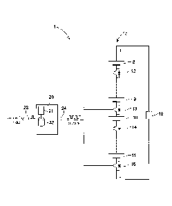
Figure 2 illustrates an example of a high voltage dc power source 1
according to the present invention. The high voltage dc power source 1,
in the following denoted dc power source 1 comprises one or more
strings 4a-c connected in parallel, each string being subdivided into a
plurality of dc power source units 8-11 connected in series. In figure 2
only one string is shown. The number of dc power source units 8-11 in
series connection depends on the desired voltage level of the dc power
source 1. Each string 4a-c is provided with at least one solid-state
switch 12-15 configured to connect and disconnect the string. In
figure 2 four switches 12-15 and four dc power source units 8-11 are
shown. It is however possible to decrease the number of switches in
each string as long as the breaking capability of the switch or switches
is/are sufficient to disconnect the string. The dc power source 1 further
comprises a control unit to turn on and off the switches. The control
CA 02824895 2013-07-16
WO 2012/097866 PCT/EP2011/050560
unit comprises one or more string control units 20, one for each string
4a-c in the dc power source 1. Since only one string is shown in figure 2
only one string control unit is shown. The string control unit controls the
turn on and the turn off of the switches in its corresponding string.
5
The string control unit 20 is configured, upon receiving a connecting
order 23 from a main controller (not shown in figure 2) to connect the
string 4a-c and thereby initiating a charging current. The string control
unit 20 includes among other things suitable processing means, such as
10 a Central Processing Unit. According to the invention the string control
unit 20 further includes a soft start module 21 configured to
simultaneously control the switches 12-15 of the string to be alternately
turned on and off so that a soft charging of an electronic device 19
connected in parallel with the string is achieved. The string control unit
20 is configured to execute the soft start module 21 upon receiving the
connecting order 23. The electronic device 19 comprises for example a
dc link capacitor in a power apparatus or another string in the dc power
source 1. In the latter case the high voltage dc power source 1 can be
used for equalising a voltage difference between parallel strings.
In a first embodiment of the invention the string control unit comprises
a memory storage 22 for storing predefined switching patterns. When
the string control unit 20 receives an order to connect the string, the
soft start module 21 will retrieve a predefined switching pattern from
the memory storage 22, and simultaneously control the switches of the
string to be alternately turned on and off in accordance with the
predefined switching pattern. The soft start module 21 is configured to
generate a control signal 24 based on the switching pattern and the
string control unit is configured to send the control signal 24 to each
switch in the string. The switching patterns define the time intervals
between turning the switches on and off and between turning the
switches off an on and is determined during the design phase of the dc
CA 02824895 2013-07-16
WO 2012/097866 PCT/EP2011/050560
11
power source based on circuit parameters such as loop inductance,
voltage level of the dc power source etc. As soon as the switches have
been turned on the charging current through the string will start to
increase. The switches are a short moment later turned off in
accordance with the predefined switching pattern in order for the
current to decrease below a second threshold value before the switches
are turned on again. This procedure is repeated in accordance with the
predefined switching pattern until a predetermined voltage value across
the electronic device is achieved.
In a second embodiment the switching pattern is not based on a
predefined switching pattern but on measurements of the charging
current. The string control unit will receive mesurennent values of the
charging current in the string from a current measuring device not
shown in figure 2. When the charging current has reached a first
threshold value the switches are turned off in order for the current to
decrease below the second threshold value before the switches are
turned on again. This procedure will be repeated until the
predetermined voltage value across the electronic device is achieved. At
that time the charging current will not be able to reach above the first
threshold value and the string will remain connected.
Figure 3a-c shows three schematical examples of switching patterns,
turning the switches in the string alternately on and off. The switching
patterns could be predefined but could also be a result of measured
values of the charging current as described above. On the x-axis of the
diagram in figure 3a-c is shown the time instants at which the switches
in the string are being simultaneously turned on and off during the soft
charging of the electronic device. A dotted line 30 shows the time
instant where the switches are being turned on for the first time after
the connection order has been sent to the string control unit. On the y-
axis of the diagram is shown the current switch status of the switches in
CA 02824895 2013-07-16
WO 2012/097866 PCT/EP2011/050560
12
the string being either ON or OFF. When the predetermined voltage
value across the electronic device has been achieved, the switches will
remain in the ON status during the operation of the dc power source. In
the diagram in figure 3a a switching pattern is shown where the time
intervals between the turn on and the turn off (switch status ON) and
the time interval between the turn off and the turn on (switch status
OFF) of the switch remains constant through the charging process.
How fast the charging current increases depends on the difference
between the voltage value across the string and the voltage value
across the electronic device and the loop inductance. In the beginning
of this charging process the difference is at its highest level and
accordingly, the charging current will reach the predefined threshold
value much faster than at the end of the charging process.
Consequently, in order to increase the speed of the charging process
the time interval when the switches are in the ON status has to increase
and this object is achieved with the switching patterns shown in figure
3b and 3c. In the switching pattern shown in figure 3b the time interval
between the turn on and the turn off remains constant through the
charging process, but the switches are turned on more frequent i.e. the
switching frequency is increased. In the switching pattern shown in
figure 3c the frequency remains constant but the time interval between
the turn on and the turn off is increased.
In figure 3d is shown the voltage value across the electronic device 19
using the switching pattern shown in figure 3c as the voltage increases
until the predetermined voltage value has been achieved.