Note: Descriptions are shown in the official language in which they were submitted.
CA 02825132 2013-07-18
WO 2012/099718
PCT/US2012/020222
1
LIGHT EMITTING DIODE SWITCH DEVICE AND ARRAY
CROSS-REFERENCE TO RELATED APPLICATIONS
Not Applicable
STATEMENT RE: FEDERALLY SPONSORED RESEARCH/DEVELOPMENT
Not Applicable
BACKGROUND
1. Technical Field
The present disclosure relates generally to touch-sensitive electronic
components and light emitting diodes (LEDs), and more particularly to an LED
switch device and array.
2. Related Art
LEDs are ubiquitous output devices that find many applications across a
variety of fields for their high efficiency, fast switching, and extended
longevity,
among other advantages. One of the most common utility is as indicators for
electronic devices, and so LEDs are available in packages of different shapes
and
sizes to suit the particular application. Additionally, different illumination
colors or
radiation wavelengths across the visible spectrum are available, from the low
wavelength red to the high wavelength violet. Several LEDs can be combined
into
arrays, with each LED being independently driven to generate visible patterns
representative of text and graphics. Beyond the visible spectrum, however,
there are
LEDs capable of emitting infrared waves, which are typically utilized for
inter-device
communications. At the opposing end of the spectrum, ultraviolet waves may be
utilized for sterilizing, sanitizing and disinfecting purposes. Although a
typical
miniature LED indicator light has an operating current of around 20mA with
less than
1 lumen of output, some recent high power LEDs are capable of operating
currents of
hundreds of mA and over a thousand lumens of output, which can serve as
substitutes
for incandescent bulbs in lighting applications.
The operational principles of LED devices are well known, with a central part
being a semiconductor material that is doped to create a P-N junction. The
anode, or
the P-side of the junction is connected to a positive terminal of a power
supply, while
CA 02825132 2013-07-18
WO 2012/099718
PCT/US2012/020222
2
the cathode, or the N-side of the junction, is connected to a negative or
common
terminal of the power supply. As electricity flows between the P-N junction,
energy in
the form of a light photon is released. Whether utilized as a miniature, low
power
indicator or as a high-intensity illuminator, LEDs operate in this manner. In
some
applications, an LED can be utilized as a photodetector, where photons of
light falling
on the P-N junction are converted to an electrical signal. Instead of being
connected to
a power supply, the LED may be connected to a detection circuit to produce a
response upon receiving a signal therefrom.
Except in the aforementioned application as a photodetector, packaged LED
devices are generally considered basic output devices. As noted, an array of
LEDs can
be devised with each one being controlled individually in order to generate
coherent
visual patterns. Direct user interactions with such visual outputs over
display arrays
have been contemplated, but such devices have involved a separate input device
that
is overlaid on the output device. One example is a capacitive touch screen
utilized in
slate computing devices such as TabletPCs from various manufacturers and the
iPad
from Apple, Inc. of Cupertino, California.
These devices are known to utilize a transparent or semi-transparent sensor
panel comprised of rows and columns of traces on opposite sides of a
dielectric. The
traces are comprised of indium tin oxide or antimony tin oxide, with a top
glass panel
being etched with the column traces and a bottom glass panel being etched with
the
row traces. For the touch sensor panel to be transparent, the etched traces
are around
microns. Separating the top glass panel and the bottom glass panel may be a
transparent polymer spacer that serves as the dielectric between the column
traces and
the row traces. The sensor panels are then mounted in an overlapping
relationship to
25 the liquid crystal display (LCD).
Another example of incorporating simultaneous input and output capabilities
in displays, albeit on a slightly larger scale, are LED matrices with switches
close to
the LEDs. One known device is disclosed in U.S. Pat. No. 5,638,052 to Furuya,
et al,
which discloses an array of LEDs with switches for turning on or turning off
30 individual LEDs being provided at locations corresponding to or close to
the LEDs.
The Sensacell device produced by Sensacell Inc. of Brooklyn, New York is
similar to
the Furuya, et al. device, except for the use of capacitive sensors disposed
amongst a
matrix of LEDs each forming a unit of inter-connectible cells.
CA 02825132 2013-07-18
WO 2012/099718
PCT/US2012/020222
3
In these earlier systems, the output or display device is configured
independently from the input device. Accordingly, there is a need in the art
for an
integrated LED switch device and array.
BRIEF SUMMARY
In accordance with various embodiments of the present disclosure, an LED
switch device is contemplated. There may be an electroluminescent
semiconductor
element with a first polarity contact and a second polarity contact. The LED
switch
device may have a first polarity lead frame, to which the electroluminescent
semiconductor element is mounted. The first polarity contact of the
electroluminescent semiconductor element may be electrically connected to the
first
polarity lead frame. Additionally, there may be a second polarity lead frame
that may
be electrically connected to the second polarity contact of the
electroluminescent
semiconductor element. There may also be a touch sensor lead frame that may be
electrically connected to a touch sensor lead.
Another embodiment of the present disclosure may be a light emitting diode
switch device. The device may include a first polarity lead. Additionally,
there may be
at least one electroluminescent semiconductor element that has a first
polarity contact
and a second polarity contact. The device may further include a first polarity
LED
lead frame with the at least one electroluminescent semiconductor element
mounted
thereto. The first polarity contact thereof may be electrically connected to
the first
polarity lead. There may also be a second polarity lead, as well as a second
polarity
LED lead frame that is electrically connected to the second polarity lead. The
second
polarity LED lead frame may be electrically connected to the second polarity
contact
of the electroluminescent semiconductor element. There may also be a first
touch
sensor lead, as well as a touch sensor lead frame to which it is electrically
connected.
The second polarity lead may be connectible to a light emitting diode driver
source.
The touch sensor lead may be connectible to a touch sensor controller input.
According to yet another embodiment of the present disclosure, there is a
combination input and output device. The device may include a light emitting
diode
driver integrated circuit that has a plurality of independent output lines.
Additionally,
there may be a touch input controller integrated circuit that has a plurality
of
independent input lines. The device may also include an array of light
emitting diode
CA 02825132 2013-07-18
WO 2012/099718
PCT/US2012/020222
4
switch devices. The light emitting diode switch device, in turn, may include a
first
electroluminescent semiconductor element electrically connected to a one of
the
plurality of independent output lines of the light emitting diode driver
integrated
circuit. The light emitting diode switch device may further include a first
integrated
touch sensor lead electrically connected to a one of the plurality of
independent input
lines of the touch input controller. The first electroluminescent
semiconductor
element and the first integrated touch sensor lead may be encapsulated into a
case.
The present invention will be best understood by reference to the following
detailed description when read in conjunction with the accompanying drawings.
BRIEF DESCRIPTION OF THE DRAWINGS
These and other features and advantages of the various embodiments disclosed
herein will be better understood with respect to the following description and
drawings, in which:
FIG. 1 is a perspective view of an LED switch device in accordance with
various embodiments of the present disclosure;
FIG. 2 is a cross sectional view of an electroluminescent semiconductor die
mounted to a lead frame;
FIG. 3A is a side view of a second embodiment of the LED switch device with
an additional electroluminescent semiconductor die;
FIG. 3B is a top view of the second embodiment of the LED switch depicted
in FIG. 3A;
FIG. 4A is a side view of a third embodiment of the LED switch device
including a pair of touch sensor contacts;
FIG. 4B is a top view of the third embodiment of the LED switch device
shown in FIG. 4A;
FIG. 5A is a side view of a fourth embodiment of the LED switch device
including a pair of touch sensor contacts and multiple electroluminescent
semiconductor dies;
FIG. 5B is a front view of the fourth embodiment of the LED switch device
depicted in FIG. 5A;
FIG. 5C is a top plan view of the fourth embodiment of the LED switch device
depicted in FIGS. 5A and 5B;
CA 02825132 2013-07-18
WO 2012/099718
PCT/US2012/020222
FIG. 6A is a top plan view of a fifth embodiment of the LED switch device
with a surface mount device (SMD) package;
FIG. 6B is a perspective view of the SMD package LED switch device shown
in FIG. 6A with a cutout view showing selected internal portions thereof;
5 FIG. 7 is
a block diagram illustrating a basic application utilizing the LED
switch device in connection with an LED output driver and a touch input
controller;
FIG. 8A is an exploded perspective of a sixth embodiment of the LED switch
device with the touch input controller embedded therein;
FIG. 8B is a perspective view of the sixth embodiment of the LED switch
device shown in FIG. 8A;
FIG. 9 is a perspective view of a control switch and a ceiling fan light
fixture
controlled thereby, with the control switch utilizing the sixth embodiment of
the LED
switch device shown in FIG. 8A and FIG. 8B being enlarged;
FIG. 10 is a block diagram showing the sixth embodiment of the LED switch
device configured to control the ceiling fan light fixture as shown in FIG. 9;
FIG. 11 shows one exemplary use of an array of LED switch devices in an
interactive greeting card;
FIG. 12 shows another exemplary use of multiple LED switch devices in a
remote controller, a top view thereof being illustrated;
FIGS. 13A and 13B are detailed schematic diagrams of a circuit of the remote
controller depicted in FIG. 12;
FIG. 14 shows a large array of LED switch devices that comprise an
interactive LED display panel;
FIG. 15 shows the LED display panel comprised of a large array of LED
switch devices utilized in a picture drawing interface;
FIG. 16 shows the LED display panel utilized in an interactive teaching
interface;
FIGS. 17A and 17B show an interactive doll that includes an array of LED
switch devices;
FIG. 18 is an exploded perspective view of an array assembly utilized in the
interactive doll of the present disclosure shown in FIG. 17A and 17B;
FIGS. 19A, 19B, and 19C are detailed schematic diagrams of a circuit of the
interactive doll;
CA 02825132 2013-07-18
WO 2012/099718
PCT/US2012/020222
6
FIG. 20 is an exploded view of a disinfecting device utilizing an array of LED
switch devices; and
FIGS. 21A, 21B, and 21C show the disinfecting device shown in FIG. 20 in
various states of use.
Common reference numerals are used throughout the drawings and the
detailed description to indicate the same elements.
DETAILED DESCRIPTION
The present disclosure contemplates a light emitting diode (LED) switching
device and array. The detailed description set forth below in connection with
the
appended drawings is intended as a description of the several presently
contemplated
embodiments of these devices, and is not intended to represent the only form
in which
the disclosed invention may be developed or utilized. The description sets
forth the
functions and features in connection with the illustrated embodiments.
However, that
the same or equivalent functions may be accomplished by different embodiments
that
are also intended to be encompassed within the scope of the present
disclosure. It is
further understood that the use of relational terms such as first and second
and the like
are used solely to distinguish one from another entity without necessarily
requiring or
implying any actual such relationship or order between such entities.
FIG. 1 illustrates one embodiment of a presently contemplated LED switch
device 10, which includes a first polarity lead 12, a second polarity lead 14,
and a
touch sensor lead 15. LEDs in general and the LED switch device 10 in
particular can
have a common-cathode or a common-anode configuration. In a common cathode
configuration, the first polarity lead 12 corresponds to a cathode while the
second
polarity lead 14 corresponds to an anode. In a common anode configuration, the
first
polarity lead 12 corresponds to an anode while the second polarity lead 14
corresponds to a cathode.
Although the embodiments disclosed herein have a common cathode
configuration, it will be appreciated by those having ordinary skill in the
art that the
contemplated features are also applicable in a common anode configuration.
Along
these lines, although various features are described as being particular to an
anode or
a cathode, the use of these terms is for purposes of consistency with respect
to the
examples presented. For example, the first polarity leads 12 are referred to
as cathode
CA 02825132 2013-07-18
WO 2012/099718
PCT/US2012/020222
7
leads in a common-cathode configuration, but in a common-anode configuration,
the
first polarity leads 12 may be appropriately referenced as anode leads.
Further, the use
of the term anode or cathode as modifiers of various components are likewise
not
intended to be limiting, particularly with respect to the direction of current
flow as
would be suggested by the use of such terms. Thus, the term anode could refer
to an
electrode through which electrical current enters the LED switch device 10, as
well as
an electrode through which electrical current exits the LED switch device 10.
The first polarity/cathode lead 12 is structurally contiguous with a first
polarity/cathode lead frame anvil 16, both of which are electrically
conductive. The
cathode lead frame anvil 16 is embedded within a case 18, which has a
generally
cylindrical configuration with a bottom end 19 and an opposed top end 21. In
further
detail, the cathode lead frame anvil 16 may be enlarged, that is, thicker
and/or wider,
in comparison to the cathode lead 12 for rigidity and support. A part of the
cathode
lead 12 are also embedded within the case 18, while other portions extend from
the
bottom end 19 of the case 18.
Also embedded within the case 18 is a second polarity/anode lead frame post
20, which is structurally contiguous with the second polarity/anode lead 14.
Like the
cathode lead 12 and the cathode lead frame anvil 16, the anode lead 14 and the
anode
lead frame post 20 are electrically conductive. The cathode lead frame anvil
16 is
structurally independent of the anode lead frame post 20, and there is an
oblique gap
22 of varying sizes and shapes defined between. Although the terms "anvil" and
"post" are used to reference certain features of the lead frames in the LED
switch
device 10, it will be recognized that this is for purposes of convenience in
differentiating between several features and not in any limiting sense. For
instance,
the anvil may also be referred to as a first polarity LED lead frame, and the
post may
also be referred to as a second polarity LED lead frame. In some cases, the
correspondence of terminology may be reversed. Those having ordinary skill in
the
art will understand that similar features, whether referred to as anvils,
posts, or by any
other term, refers to the same basic structure described herein.
Another component embedded within the case 18 is a touch sensor lead frame
23, which is structurally contiguous with the touch sensor lead 15. Again,
like the
other leads, lead frame posts, and lead frame anvils discussed above, the
touch sensor
lead 15 and the touch sensor lead frame 23 are electrically conductive. The
anode lead
CA 02825132 2013-07-18
WO 2012/099718
PCT/US2012/020222
8
14 and the touch sensor lead 15 also extend from the bottom end 19 of the case
18. In
some contemplated embodiments, the touch sensor lead 15 may be configured
similarly to the anode lead 14 except for the pertinent features thereof that
will be
discussed more fully below. The touch sensor lead frame 23 may be configured
similarly to the anode lead frame post 20, in that there are no
electroluminescent
semiconductor dies 28 mounted thereon. Indeed, in these embodiments, these
components may be a repurposed anode lead 14 and anode lead frame post 20.
With additional reference to FIG. 2, a top portion 24 of the cathode lead
frame
anvil 16, which faces the top end 21 of the case 18, defines a die mounting
crater 26.
In accordance with various embodiments of the LED switch device 10, an
electroluminescent semiconductor die 28 is attached to the cathode lead frame
anvil
16 and in particular disposed within the die mounting crater 26. In some
configurations, the die mounting crater 26 has a reflective surface, though
this is
optional. The electroluminescent semiconductor die 28 has a first
polarity/cathode
contact 30, and a second polarity/anode contact 32. As discussed above, the
electroluminescent semiconductor die 28 has a P-N junction from which photons
of
light are emitted at a particular wavelength as electrons flows through holes
therein as
the energy level is lowered. Thus, the cathode contact 30 is the negative
electrode,
while the anode contact 32 is the positive electrode. It is understood that
the emitted
wavelength or color may be varied by changing the material of the P-N
junction,
specifically based upon its band-gap energy.
FIG. 2 illustrates the electroluminescent semiconductor die 28 being mounted
directly onto the cathode lead frame anvil 16. The electrical connection to
the N-side
electrode of the P-N junction, however, is made through the cathode contact 30
and a
first wire bond 34. It is also known to connect the cathode contact 30
directly to the
cathode lead frame anvil 16.
As indicated above, the LED switch device 10 in accordance with various
embodiments includes a plurality of second polarity/anode lead frame posts 20.
The
first anode lead frame post 20a, otherwise referred to as an LED lead frame
post
because of its function, is electrically connected to the anode contact 32 of
the
electroluminescent semiconductor die 28, and hence the P-side electrode of the
P-N
junction, over a second wire bond 36. Thus, the circuit from the anode lead 14
and the
CA 02825132 2013-07-18
WO 2012/099718
PCT/US2012/020222
9
anode lead frame post 20, to the electroluminescent semiconductor die, to the
cathode
lead frame anvil 16 and the cathode lead 12 is completed.
The mounting orientation and the surface of the electroluminescent
semiconductor die 28 may be optimized for reflecting the maximum amount of
light
in one or more desired directions. In this regard, because the top end 21 of
the case 18
is the typical emission direction, the electroluminescent semiconductor die 28
is
oriented thus. For additional focusing of the emitted light, the case 18 may
include a
lens 38 that focuses the emitted light. In further detail, it is contemplated
that the case
18 is constructed of a transparent or at least translucent epoxy material that
may be
colored to match that of the emitted light.
Although a single electroluminescent semiconductor die 28 that emits one
color is shown in FIG. 1 and FIG. 2, it will be recognized that any number of
additional ones may be included in the LED switch device 10. Generally, a
first one
of the electroluminescent semiconductor dies 28 may correspond to a first
visible
spectrum wavelength emission, and a second one of the electroluminescent
semiconductor dies 28 may correspond to a second visible spectrum wavelength
emission, where the first emitted wavelength is different than the second
emitted
wavelength. In one exemplary embodiment, the electroluminescent semiconductor
dies for the colors red, green, and blue may be incorporated into the LED
switch
device 10 to generate different hues of light that are combinations of these
primary
colors.
Referring again to FIG. 1, the LED switch device 10 includes the touch sensor
lead frame 23 that is structurally independent of the anode lead frame post 20
and
electrically isolated from the same. Furthermore, the touch sensor lead frame
23 may
be connected to the touch sensor lead 15. The touch sensor lead frame 23 may
be
disconnected from the electroluminescent semiconductor die 28. While it is
possible
to mount an electroluminescent semiconductor die 28 to the touch sensor lead
frame
23, so long as the circuit therefor is not completed, i.e., there are no
connections to a
power source and/or to ground, it is understood that such electroluminescent
semiconductor die will remain largely non-functional.
The touch sensor lead frame 23 is connected to a touch sensor contact 39 that
is contemplated to serve as an electrode for measuring body capacitance. It is
understood the human body in general, and appendages thereof such as fingers
in
CA 02825132 2013-07-18
WO 2012/099718
PCT/US2012/020222
particular, typically have a capacitance of around 22pF. As will be discussed
in
further detail below, the capacitance thus detected by the touch sensor
contact 39 can
be ascertained using additional input control circuitry per various modalities
known in
the art. Thus, as a finger is pressed against or moved into the proximity of
the surface
5 of the case 18, the capacitance detected on the touch sensor contact 39
changes, with
this input being usable for triggering additional functionality. In accordance
with the
embodiment of the LED switch device 10 shown in FIG. 1, the touch sensor lead
frame 23 is extended further towards the top end 21 of the case 18. The touch
sensor
contact 39 is embedded within the case 18 and extends substantially around the
10 circumference of the same, and is connected to the touch sensor lead
frame 23. As
such, it is envisioned that a finger placed on or placed in the proximity of
any portion
of the lens 38 is detectable.
Several different variations of the LED switch device 10 are contemplated.
With reference to FIG. 3A and FIG. 3B, a second embodiment of the LED switch
device 10b includes an alternatively shaped cathode lead frame anvil 16, which
is
structurally contiguous with the cathode lead 12. Attached to the die mounting
crater
26 is a first electroluminescent semiconductor die 28a and a second
electroluminescent semiconductor die 28b. As briefly indicated above, emitting
a
plurality of different colors/wavelengths from the single LED switch device 10
is
possible by adding another LED element. In this particular example, the first
electroluminescent semiconductor die 28a may emit a red color wavelength
light,
while the second electroluminescent semiconductor die 28b may emit either a
green
or blue color wavelength light. For separate control of these
electroluminescent
semiconductor dies 28a, 28b, amongst the first subset of anode lead frame
posts 20,
there is a first one 20a that is electrically connected to the first
electroluminescent
semiconductor die 28a over a wire bond and a second one 20b that is
electrically
connected to the second electroluminescent semiconductor die 28b also over a
wire
bond. The first anode lead frame post 20a is structurally contiguous with the
first
anode lead 14a, while the second anode lead frame post 20b is structurally
contiguous
with a corresponding second anode lead 14b.
As with the first embodiment of the LED switch device 10 discussed above,
the second embodiment 10b includes the touch sensor lead frame 23 that is
connected
to the one touch sensor contact 39. Again, the touch sensor lead frame 23 is
CA 02825132 2013-07-18
WO 2012/099718
PCT/US2012/020222
11
structurally contiguous with the touch sensor lead 15. The touch sensor
contact 39 is
disposed toward the top end 21 of the case 18, and defines a partial loop
around its
circumference. Furthermore, each of the aforementioned components are embedded
within a transparent or at least translucent case 18.
A third embodiment of the LED switch device 10c is shown in FIGS. 4A and
4B. Similar to the previously described embodiments, there is the cathode lead
frame
anvil 16 that is structurally contiguous with the cathode lead 12. Again,
attached to
the die mounting crater of the cathode lead frame anvil 16 is the
electroluminescent
semiconductor die 28. Since there is only one electroluminescent semiconductor
die
28, only a single color wavelength is emitted, and is driven by an electrical
current
delivered to the single anode lead frame post 20, which is structurally
contiguous with
the anode lead 14.
Instead of a single touch sensor contact 39, the third embodiment of the LED
switch device 10c contemplates two separate ones that are alternatively
configured. In
further detail, a first touch sensor contact 42 has a semicircular
configuration and
extends inwardly towards the center axis of the case 18. Additionally, a
second touch
sensor contact 44 is laterally opposite the first touch sensor contact 42 but
has the
same semicircular configuration and extends inwardly towards the center axis
of the
case 18. The first touch sensor contact 42 is structurally contiguous with a
first touch
sensor lead frame 23a as well as a first touch sensor lead 15a. The second
touch
sensor contact 44, in turn, is structurally contiguous with the second touch
sensor lead
frame 23b and the second touch sensor lead 15b. There being two separate touch
sensor contacts 42, 44, it is understood that any touch inputs can be
separately or
simultaneously registered, thereby providing an additional degree of
precision.
With reference to FIGS. 5A, 5B, and 5C, a fourth embodiment of the LED
switch device 10d includes the cathode lead frame anvil 16, on which a first
electroluminescent semiconductor die 28a, a second electroluminescent
semiconductor die 28b, and a third electroluminescent semiconductor die 28c
are
mounted. In this embodiment, it is contemplated that the full color spectrum
is
reproducible using the primary colors of red, green, and blue, so these three
electroluminescent semiconductor dies 28a-c correspond thereto. The cathode
lead
frame anvil 16 is structurally contiguous with the cathode lead 12. The
CA 02825132 2013-07-18
WO 2012/099718
PCT/US2012/020222
12
electroluminescent semiconductor dies 28a-c are independently controllable, as
will
be described below.
As best illustrated in FIG. 5A, there is a first anode lead frame post 20a
that is
structurally contiguous with the first anode lead 14a. Additionally, there is
a second
anode lead frame post 20b that is structurally contiguous with the second
anode lead
14b, as well as a third anode lead frame post 20c that is structurally
contiguous with
the third anode lead 14c. It is understood that the first anode lead frame
post 20a, the
second anode lead frame post 20b, and the third anode lead frame post 20c are
electrically connected to a respective one of the first electroluminescent
semiconductor die 28a, the second electroluminescent semiconductor die 28b,
and a
third electroluminescent semiconductor die 28c over individual wire bonds. The
anode lead frame posts 20 are oriented along a single lateral axis.
FIG. 5B and FIG. 5C best illustrate a first touch sensor lead frame 23a and a
second touch sensor lead frame 23b that are oriented in a perpendicular
relationship to
the anode lead frame posts 20 described above. However, it is possible for
these touch
sensor lead frames 23 to be oriented along a single lateral axis as the anode
lead frame
posts 20. The first touch sensor lead frame 23a is structurally contiguous
with a first
touch sensor lead 15a as well as the first touch sensor contact 42. The second
touch
sensor lead frame post 23b is structurally contiguous with a second touch
sensor lead
15b and the second touch sensor contact 44. Like the third embodiment of the
LED
switch device 10c described above, the first touch sensor contact 42 has a
semicircular
configuration that is opposed to the second touch sensor contact 44, which
also has a
semicircular configuration. The first touch sensor lead frame post 23a has a
bent
section 43 that extends the coverage area of the first touch sensor contact
42. The
second touch sensor lead frame post 23b similarly has a corresponding bent
section 45
for extending the second touch sensor contact 44 toward the outer portion of
the case
18.
As can be seen from the forgoing examples, the LED switch device 10 can be
configured in numerous ways, particularly with respect to the configuration of
electroluminescent semiconductor dies 28 and the touch sensor contact 39 or
touch
sensor contacts 42, 44. These examples are not intended to be limiting, and
based
upon a proper understanding of the present disclosure, those having ordinary
skill in
the art will be capable of developing further alternatives.
CA 02825132 2013-07-18
WO 2012/099718
PCT/US2012/020222
13
The foregoing examples are all configured as through-hole cylindrical
packages suitable for installation on conventional printed circuit boards.
With
reference again to FIG. 1, the leads 12, 14 include stop tabs 46 that limit
the extent of
insertion into the holes on the printed circuit board. However, it will be
appreciated
that the features of the LED switch device 10 can be incorporated into any
package
shape including round dome top, round flat top, rectangular flat top,
triangular or
square flat top, and so forth. Among these different shapes, various sizes are
also
possible. Likewise, the orientation of the touch sensor contacts 42, 44 as
well as the
various leads, including the first polarity lead 12, the second polarity lead
14, and the
touch sensor lead 15 may extend from the case 18 in various directions, such
as from
the side, at an angle, and so forth. Those having ordinary skill in the art
will
appreciate that the specific form factors presented are by way of example, and
based
upon the features disclosed in the context of such specific form factors, the
features
may be readily implemented in alternative form factors, whether presently
known or
unknown.
As best shown in FIGS. 6A and 6B, another embodiment of the LED switch
device 10e contemplates the use of a surface mount device (SMD) package. More
particularly, there is a carrier 48 with leads 50a-50f extending therefrom for
connecting to external components. In the illustrated embodiment, there is the
first
electroluminescent semiconductor die 28a with a first illumination color, the
second
electroluminescent semiconductor die 28b with a second illumination color, and
the
third electroluminescent semiconductor die 28c with a third illumination
color. The
sixth lead 50f is structurally contiguous and electrically common with a sixth
lead
frame 51f, on which the first electroluminescent semiconductor die 28a is
mounted,
and to which it is electrically connected. The fifth lead 50e is structurally
contiguous
and electrically common with a fifth lead frame 51e, on which the second
electroluminescent semiconductor die 28b is mounted, and to which it is
electrically
connected. Furthermore, the fourth lead 50d is structurally contiguous and
electrically
common with a fourth lead frame 51d, on which the third electroluminescent
semiconductor die 28c is mounted, and to which it is electrically connected.
The
second lead 50b is structurally contiguous and electrically common with a
second lead
frame 51b, which serves as a common anode for the electroluminescent
semiconductor dies 28a-c. The anodes of each of the electroluminescent
CA 02825132 2013-07-18
WO 2012/099718
PCT/US2012/020222
14
semiconductor dies 28a-c is electrically connected to the second lead frame 5
lb over
respective wire bonds 34a-c, while the contacts with the lead frames 51d, 51e
and 51f,
respectively, are made on the cathodes of the electroluminescent semiconductor
dies
28a-c by means of a conductive adhesive.
The LED switch device 10e also includes the first touch sensor contact 54a
that is mounted to and electrically common with a first lead frame 51a, also
referred
to as a first touch sensor lead frame 47a. The third lead 50c is understood to
be
structurally contiguous with the third lead frame 51c. Additionally, the
second touch
sensor contact 54b is mounted to and electrically common with a third lead
frame 51c,
also referred to as a second touch sensor lead frame 47b. The third lead frame
51c is
structurally contiguous with the third lead 50c. The size, shape and general
configuration or form factor of the touch sensor contacts 54 and touch sensor
lead
frames 47 employed in the LED switch device 10e are presented by way of
example
only, and may be differently configured than as shown in FIG. 6B.
The carrier 48 may encapsulate portions of the various lead frames 5la-f, and
the electroluminescent semiconductor dies 28a-28c are disposed within the
same. The
carrier 48, however, defines an opening 55 through which the touch sensor
contacts
54 and/or the electroluminescent semiconductor dies 28 are exposed. There is a
transparent or partially translucent case 52 that encapsulates such
components. In
some embodiments of the SMD package, portions or the entirety of the touch
sensor
contacts 54 may be encapsulated within the carrier 48, and may not be exposed
through the case 52. It will be appreciated that although the structural
design and form
factor of a specific surface mount package has been shown and described, other
structural designs and form factors of surface mount packages may be utilized.
Having considered the basic parts of several embodiment of the LED switch
device 10, one exemplary use thereof will now be described. With reference to
the
block diagram of FIG. 7, the LED switch device 10 is connected to an LED
driver 56
as well as a touch input controller 58. In one embodiment, the touch input
controller
58 is the eKT2101 capacitive touch pad controller integrated circuit from Elan
Microelectronics Corp. of Hsinchu, Taiwan. It is understood that the LED
driver 56
generates an electrical signal on an output line 57 that is transmitted
through the
anode lead 14 and the anode lead frame post 20, activating the
electroluminescent
semiconductor die 28 in accordance with conventional techniques. Additionally,
it is
CA 02825132 2013-07-18
WO 2012/099718
PCT/US2012/020222
understood that an input line 59 of the touch input controller 58 is connected
to the
touch sensor lead 15 and the touch sensor lead frame 23, with the touch input,
that is,
the corresponding capacitance change on the touch sensor contact 39, being
detected.
Though further details will follow, the output from the LED driver 56 can be
initiated
5 by a data
processing device 60 or controller. Furthermore, the touch input controller
58 can generate a data signal indicative of a touch input upon detection
thereof, and
that data signal can be transmitted to the data processing device 60. Based on
such
touch inputs and possibly other types of inputs, appropriate responses to the
LED
driver 56 can be generated.
10 In the
embodiment discussed above, the touch input controller 58 is
understood to be separate from the LED switch device 10. However, as
illustrated in
FIG. 8A and FIG. 8B, yet another embodiment of the LED switch device 10f
includes
an embedded printed circuit board 62 with an LED switch device controller
integrated
circuit 64 mounted thereto. It is contemplated that the LED switch device
controller
15 integrated
circuit 64 incorporates the functionality of the LED driver 56, the touch
input controller 58, and the data processing device 60 into a single package.
Like the
other variations, the first electroluminescent semiconductor die 28a and the
second
electroluminescent semiconductor die 28b are embedded within the case 18,
though
they are mounted to the printed circuit board 62.
A power lead 180 and the ground lead 182 are attached to the printed circuit
board 62, and are understood to supply power/ground to the LED switch device
10f.
In particular, power and ground connections of the LED switch device
controller
integrated circuit 64 are in electrical communication with the power lead 180
and the
ground lead 182. Power to drive the touch input controller 58, the LED driver
56, and
the data processing device 60 is understood to be supplied thereby.
As noted above, the first touch sensor contact 42 and the second touch sensor
contact 44 are electrodes that are utilized for detecting capacitance changes,
and in
and of themselves do not generate signals that are typical of data
transmissions for the
data processing device 60. The LED switch device controller integrated circuit
64 is
understood to detect the capacitance change. In the LED switch device 10f,
there are
understood to be two electrodes, the first touch sensor contact 42 and the
second
touch sensor contact 44, which are connected to independent inputs of the LED
switch
device controller integrated circuit 64.
CA 02825132 2013-07-18
WO 2012/099718
PCT/US2012/020222
16
The LED switch device 10f has two outputs, that is, a first output lead 168
and
a second output lead 169. A signal indicating that the first touch sensor
contact 42 was
activated can be generated on the first output lead 168, while another signal
indicating
that the second touch sensor contact 44 was activated can be generated on the
second
output lead 169. With the functionality of the data processing device 60
embedded
into the LED switch device 10f, other outputs besides such a simple indicator
directly
tied to the touch input controller 58 may be generated. In other words, the
output
generated at the output leads 168, 169 may be independent of the inputs
detected by
the touch sensor contacts 42, 44. As will be described in further detail
below, the
touch input as detected by the touch input controller 58 may be further
processed to
control various external devices. Thus, it is expressly contemplated that
additional
output leads may be provided.
In addition to the two outputs, the LED switch device 10f also has an input
lead 170, through which various external inputs may be connected. The inputs
received may be utilized to control the lighting of the electroluminescent
semiconductor devices 28a, 28b, though again, because of the incorporation of
the
functionality of the data processing device 60, more sophisticated responses
beside an
activation or a deactivation may be generated, such as dimming, color mixing,
flashing, and so forth.
Because touching one of the first touch sensor contact 42 or second touch
sensor contact 44 generates a different response from the LED switch device
controller integrated circuit 64, additional visual segregation thereof is
contemplated.
The top end 21 of the case 18 has a concave surface with an oval outline that
is
divided into a first segment 172 and a second segment 174. Thus, touching the
first
segment 172 is understood to trip the first touch sensor contact 42 that
results in an
output being generated on the first output lead 168, while touching the second
segment 174 trips the second touch sensor contact 44 with an output generated
on the
second output lead 169. Touching both the first segment 172 and the second
segment
174 simultaneously may result in an output on both the first output lead 168
and the
second output lead 169. For the most part, the output from the two
electroluminescent
semiconductor dies 28 are independent of any touch input, as they are
separately
controlled from a data processing device 60 in response to the touch input.
CA 02825132 2013-07-18
WO 2012/099718
PCT/US2012/020222
17
Although simple on/off functionality is described herein, it will be
appreciated
by those having ordinary skill in the art that a finer degree of receptiveness
to touch
input is possible, such as partial placement, swiping from one to the other,
and so
forth. Variations on the incorporation of multiple functions into the single
package of
the LED switch device 10 are understood to be within the purview of those
having
ordinary skill in the art.
As will become apparent, the LED switch device 10 and its different
configurations may be utilized in a wide variety of applications. With
reference to
FIG. 9, the aforementioned LED switch device 10f may be utilized as a wall-
mounted
control switch 220, to control the various functions of a ceiling fan light
fixture 222.
Referring additionally to the block diagram of FIG. 10, the ceiling fan light
fixture
222 includes fan blades 224 spun by an electric motor 226. Due to the high
current
requirements to drive the electric motor 226, there is a fan driver circuit
228 that
draws power separately from an external source. Along these lines, the ceiling
fan
light fixture 222 includes lamps 230 that illuminates the room upon
activation. Like
the electric motor 226, the lamps 230 have higher current/power requirements
than
that which can be supplied by the LED switch device 10f, so there is lamp
driver
circuit 232 that draws power from an external source. The fan driver circuit
228 and
the lamp driver circuit 232 are controlled by the LED switch device 10f based
upon
the inputs received thereon, and can include rotation speed changes (fast,
medium,
slow) of the fan blades 224, as well as the intensity/dimming level of the
lamps 230.
Feedback that indicates the actual lighting level of the lamps 230 can also be
generated by the lamp driver circuit 232 back to the LED switch device 10f.
The fan
blades 224, the electric motor 226, and the fan driver circuit 228 will be
collectively
referenced as a fan unit 229, while the lamps 230 and the lamp driver circuit
232 will
be collectively referenced as a lamp unit 233. It will be recognized that the
fan unit
229 and the lamp unit 233 may include further additional components, however.
The control switch 220 includes a conventional wall panel 234, within which a
receptacle 236 is defined. An LED switch assembly 238 mounted to the wall
panel
234. The wall panel 234 may have been previously secured to a wall structure
239,
and so the LED switch assembly 238 is contemplated to be a simple
replacement/retrofit for mechanical switches and the like that may have been
installed
therein.
CA 02825132 2013-07-18
WO 2012/099718
PCT/US2012/020222
18
The LED switch assembly 238 includes the centrally mounted LED switch
device 10f, as well as a backlit status indicator 240. As indicated above, the
LED
switch device 10f may include the first electroluminescent semiconductor die
28a,
which may have a red colored illumination. Further, the second
electroluminescent
semiconductor die 28b may have a green colored illumination. By way of
example,
the two colors may be utilized as an indicator of which one of the fans or the
lights are
to be controlled by any inputs received on the LED switch device 10f in that
state. For
instance, a red color illumination may indicate that the lamps 230 will be
controlled,
while a green color illumination may indicate the fan unit 229 will be
controlled.
Swiping a finger from the first segment 172 to the 174 is representative of
decreasing
power, which in the case of the lamp unit 233 being controlled, dims the
illumination
level thereof. In the case of the fan unit 229 being controlled, the rotation
speed of the
electric motor 226 is lowered. The more the touch remains on the second
segment
174, the further the lighting is dimmed/motor speed is reduced. Swiping the
finger in
the opposite direction from the second segment 174 to the first segment 172
may
cause an increase in brightness/speed. Tapping both the first segment 172 and
the
second segment 174 quickly may result in the lamp unit 233 or the fan unit 229
being
turned on or turned off at once. Pressing and holding both the first segment
172 and
the second segment 174 may switch the control mode from the lamp unit 233 to
the
fan unit 229, and vice versa. These control sequences can be programmed on the
data
processing device 60 as a set of executable instructions of detected inputs
and
generated responses. Although a specific control sequence has been described,
it will
be appreciated that any other control sequences may be implemented as
different
instructions that are executed by the data processing device 60.
Another application of the LED switch device 10 is shown in FIG. 11, which
is a greeting card 70 that includes a printed depiction of a cake with
candles. The card
70 defines cutouts 72 through which the LED switch devices 10 are shown, and
correspond to the location of the depicted candle flames. Thus, the
illuminated LED
switch devices 10 are intended to mimic the appearance of lit candles.
Alternating
colors may be utilized for different LED switch devices 10. Initially, all of
the LED
switch devices 10 may be illuminated upon opening the card 70 via a contact
switch
74. The recipient's fingers can be passed over the LED switch devices 10 for
deactivation, thereby simulating the "blowing out" of the candles. In general,
this
CA 02825132 2013-07-18
WO 2012/099718
PCT/US2012/020222
19
embodiment illustrates the use and basic configuration of an array 78 of LED
switch
devices 10 that are each controlled by the LED driver source based upon inputs
received by the touch input controller 58.
Varying operating patterns are possible with the greeting card 70. It is
contemplated that the LED switch devices 10 have at least two
electroluminescent
semiconductor dies 28 with one for the red color, and the other for either a
blue or a
green color. When the greeting card 70 is first opened, all of the LED switch
devices
may be turned on with the red color, and optionally flashing. A simple musical
score may be generated, and the recipient's fingers can be passed over the LED
10 switch
devices 10 to activate the secondary color of the electroluminescent
semiconductor die 28. Thus, with the red and the blue colors activated, there
is a pink
colored resultant output, while with the red and green colors activated, there
is a
yellow colored resultant output. The activation sequence may be recorded while
the
musical score is playing, and that sequence may be replayed after a delay or
after the
music score concludes. Without the recording functionality, touching the LED
switch
devices 10 may be operative to activate the secondary color.
FIG. 12 shows another application of the LED switch devices 10 in a remote
controller 80, which generally has inputs corresponding to a forward direction
82, an
opposed reverse direction 84, a leftward direction 86, and a rightward
direction 88.
The remote controller 80 is comprised of a case 90 held within the hands 92 of
the
user. The case 90 and has a generally flat front surface 91, including a
transparent or
translucent Mylar sheet or film 93 overlaid on the LED switch devices 10. The
sheet
93 may have various symbols and characters imprinted thereon that variously
represent the functionality that can be invoked by the underlying LED switch
devices
10. It will also be recognized that the sheet 93 may have transparent or semi-
transparent portions, and opaque portions corresponding to the imprinted
symbols and
characters. An underlying opaque base sheet with cutouts may be provided.
For the forward direction 82, there is a single forward direction LED switch
device 94, and for the reverse direction 84, there is a single reverse
direction LED
switch device 96, both of which are mounted underneath the sheet 93 of the
case 90.
By positioning the fingers over the LED switch devices 94, 96, a signal
representative
thereof can be generated and transmitted to a base receiver via radio
frequency.
CA 02825132 2013-07-18
WO 2012/099718
PCT/US2012/020222
For the sideways directions 86, 88, there is an array 98 comprised of a first
LED switch device 100a, a second LED switch device 100b, a third LED switch
device 100c, a fourth LED switch device 100d, and a fifth LED switch device
100e.
Each of these LED switch devices 100 are mounted underneath the sheet 93, and
may
5 have
different emission colors. The degree of turning is variable, and depends on
which of the five LED switch devices 100 is activated by positioning the
fingers over
the same. Alternatively, the rate at which the finger is swept from left to
right or vice
versa may determine the degree of turning exhibited by the receiving device.
The remote controller 80 can be used as a control modality for a number of
10
interactive systems, including radio-controlled vehicles and toys, video
games, and so
forth. As illustrated above, the inputs provided can be simple on/off, and
various
degrees of input can be provided by utilizing an array of multiple LED switch
devices
10.
In relation to its functions, the remote controller 80 is understood to have a
15 similar
basic architecture as described above with reference to the block diagram of
FIG. 7. With reference to the schematic diagram of FIG. 13A and 13B, there is
a
microcontroller or data processing device 60. As briefly noted above, the data
processing device 60 is configured to execute a series of preprogrammed
instructions
that generates certain outputs based upon provided inputs. The data processing
device
20 60 is
understood to have an arithmetic logic unit, various registers, an instruction
decoder, and a control unit, as is typical of data processing devices. An
internal
random access memory may also be included, as well as read-only memory that is
used to pre-store frequently utilized data such as speech and movement
sequences. By
way of example, the programmable data processing device 60 is 16-bit digital
signal
processing (DSP) integrated circuit. One commercially available option is the
eSL
Series IC from Elan Microelectronics Corporation of Hsinchu, Taiwan, though
any
other suitable IC devices may be readily substituted.
In further detail, the data processing device 60 has at least one input port
201
and a plurality of output ports 202. The output ports 202 are connected to the
LED
switch devices 10 as well as the touch input controller 58, as will be
detailed below.
In the illustrated embodiment, the anode of the electroluminescent
semiconductor
device is connected to power, while its cathode is connected to a collector of
a
transistor. The base of the transistor is connected to the output port 202 of
the data
CA 02825132 2013-07-18
WO 2012/099718
PCT/US2012/020222
21
processing device 60; thus, when the transistor is biased on by a high voltage
generated on the output port 202, the electroluminescent semiconductor (and
hence
the LED) is turned on. On the other hand, when the transistor is biased off by
a low
voltage on the output port 202, the LED is turned off.
The touch sensor leads 15 of the LED switch device 10 are connected to the
touch input controller 58, which detects capacitance changes as indicated
above.
Upon detection, a corresponding signal is generated as an output, which is
passed to
the input port 201 of the data processing device 60, labeled as PA7. In
further detail,
the data processing device 60 communicates with the touch input controller 58
over
the Serial Peripheral Interface (SPI) inter-device communications modality.
Thus,
being a serial communications system, a single data input port 201 is
utilized. A first
output port 202a for the chip select line (TPreg) is connected to the touch
input
controller 58 (and specifically pin 4 thereof) for indicating to the touch
input
controller 58 that the data processing device 60 is ready to receive data.
Furthermore,
second output port 202b, designated for the serial clock line (SCK) is also
connected
to the touch input controller 58 (and specifically pin 21 and 24 thereof) to
provide a
clock synchronization signal. A third output port 202c for the serial data out
line
(SDO) is connected to pin 20 of the touch input controller 58, and this is
understood
to be for purposes of compliance with the master-slave arrangement as dictated
by the
SPI standard. The signal to the input port 201, designated as the serial data
in line
(SDI) is connected to pin 22 of touch input controller 58, and is contemplated
to
include data relating to the identity of the LED switch device 10 upon which
an input
was detected, and so forth. Other data relating to the functioning of the
touch input
controller 58 may be communicated as well.
It is contemplated that the data processing device 60 is programmed with
executable instructions that generate specific outputs to the output ports 202
and
reflected in the LED switch devices 10 connected thereto, in response to
inputs from
the touch input controller 58 that are generated upon a detected touch on the
LED
switch devices 10. Thus, certain LEDs can be turned on or off when touched, as
discussed above in relation to the greeting card 70. Furthermore, the
functionality
provided by the remote controller 80 with respect to the activation and
deactivation of
the on-board LEDs are implemented by the data processing device 60.
CA 02825132 2013-07-18
WO 2012/099718
PCT/US2012/020222
22
Various other functionalities are contemplated for the remote controller 80.
As
briefly mentioned above, the remote controller 80 can transmit instructions to
a base
receiver. Such data transmission functions are handled by a radio frequency
transceiver integrated circuit 204. The operating frequency thereof is
understood to be
around 2.4 GHz, though any others may be substituted. Along these lines, RF
transmission is not necessary, and other wireless or wired transmission
modalities
may be substituted. In addition to data transmission, the remote controller 80
includes
a force feedback feature enabled by a motor 206 that is also connected to the
data
processing device 60. Similarly, sound output is generated through a
piezoelectric
buzzer 208 and/or a loudspeaker 210. If desired, sound inputs can be provided
to the
data processing device 60 through the piezoelectric buzzer 208 and/or a
microphone
212.
The application of the LED switch devices 10 is understood to be scalable.
With reference to FIG. 14, a wall-mounted LED display panel 102 is comprised
of
rows and columns of LED switch devices 10 capable of emitting a wide range of
colors across the visible spectrum. The LED display panel 102 is configured to
display images by activating and deactivating the LED switch devices 10 with
particular colors and intensities. By way of example, the interface shown on
the LED
display panel 102 is segregated into a left column 104 and a right column 106,
which
include icons 108, 110, respectively.
Selecting one of the icons 108 in the left column 104 is understood to select
a
specific animation of a feature of a character 112 displayed on the LED
display panel
102. As utilized herein, the selection or touching of one of the icons 108 is
understood
to refer to placing a body part on or in close proximity to one or more LED
switch
devices 10 in the LED display panel 102 that correspond to those outputting
that
specific one of the icons 108. In one contemplated sequence, touching a first
left
column icon 108a activates the animation of a mouth 114, while touching a
second
left column icon 108b activates the animation of ears 116. Touching a third
left
column icon 108c activates the animation of legs 118, and selection of a
fourth left
column icon 108d activates the animation of a tail 120. Upon touching any of
the
icons 108, visual feedback is provided by placing an emphasis thereon, such as
by, for
example, highlights.
CA 02825132 2013-07-18
WO 2012/099718
PCT/US2012/020222
23
Touching one of the icons 110 in right column 106, on the other hand, is
understood to select a particular output sound signal. Touching a first right
column
icon 110a is understood to generate a trumpet sound, and touching a second
right
column icon 110b generates a "spring" or "boing" type sound. Furthermore,
touching
a third right column icon 110c generates a bike horn sound, while touching a
fourth
column icon 110d generates a drum sound.
In another embodiment illustrated in FIG. 15, the LED display panel 102 may
be configured as picture drawing interface 250. As indicated above, the LED
display
panel 102 is an array of LED switch devices 10 arranged in rows and columns,
and
can emit a wide range of colors across the visible spectrum. Again, various
images
can be displayed by activating and deactivating certain LED switch devices 10.
In the
contemplated picture drawing interface 250, the screen area is segregated into
an
upper drawing board section 252 and a lower color palette section 254 that
displays a
series of icons 256, with each having a different color. Thus, it is
contemplated that
the lower palette section 254 resembles a conventional artist's color palette.
Selection
of one of the icons 256 is understood to select that corresponding color for
use, as will
be described in further detail below.
Touching a first color icon 256a allows the user to "draw" on the drawing
board section 252 in the selected color. That is, when the user touches or
comes into
close proximity with a particular LED switch device(s), then that one will be
illuminated with the selected color. It is contemplated that selecting a
second color
icon 256b will change the drawing color with the newly selected color. Again,
as the
user touches or comes into close proximity with a particular LED switch
device(s), it
will be illuminated with such color. In addition, there may be an eraser icon
258 that,
when selected, alters the response of the touched LED switch devices 10 to
deactivate
rather than activate with a selected color when the color icon 256 is
otherwise selected
or activated. Variations on standard touch inputs are possible as mentioned
above, and
in the present context of the picture drawing interface 250, holding the erase
icon 258
for a predetermined length of time may deactivate the entirety of the LED
display
panel 102. The LED display panel 102 can be further miniaturized for enhanced
portability.
In the particular exemplary embodiment shown in FIG. 16, a teacher 260 may
utilize the LED display panel 102 in a classroom as an interactive teaching
interface
CA 02825132 2013-07-18
WO 2012/099718
PCT/US2012/020222
24
251 to instruct a student 262 visually on a variety of different subjects. For
instance,
the concepts of shapes and colors may be taught by directing the student 262
to draw
different shapes in different colors, including a rectangle 264 in a first
color, a triangle
266 in a second color, and a circle 268 in a third color.
Additionally, the student 262 may be taught about words, letters, and numbers
by drawing such characters on the display panel 102. For further
functionality, it is
possible to connect the LED display panel 102 to a data processing device,
such that a
software application capable of character recognition may be executed thereby.
Based
upon the inputs on the LED display panel 102, the letters and words
represented by
certain sequence of inputs may yield responsive outputs. By way of example
only and
not of limitation, such outputs may be the pronunciation of inputted and
recognized
letters and words. In the case of mathematics instruction, the numbers and/or
formulas
270 being drawn on the LED display panel 102 may be verified or corrected,
with
appropriate sound and visual outputs being generated upon a correct or
incorrect
input. Such sound outputs may include a "cheering" sound when correct, or an
"uh-
oh" exclamation when incorrect. Thus, the interactive teaching interface 251
engages
both the teacher and the student to greatly enhance teaching effectiveness and
learning
enjoyment.
It will be appreciated that numerous educational and entertainment
applications are possible.
Although only a moderately sized LED display panel 102 on the order of a
human body is illustrated in FIGS. 14, 15, and 16, larger ones that span the
entirety of
walls and the like are also envisioned. It is understood that the graphics
generated on
such panels 102 may be varied considerably, as are the way such graphics are
generated in response to various types of user input. Furthermore, the LED
display
panel 102 may be utilized as a remote control or an interface for larger
conventional
LED display panels, where the input and the responses generated on the LED
display
panel 102 are transmitted to the larger display panel to be displayed.
Other, more sophisticated play patterns utilizing the LED switch device 10 are
also envisioned. With reference to FIG. 17A, an anthropomorphized interactive
bear
doll 122 has a body section 124, a pair of legs 126, a pair of arms 128, and a
head
130. As will be appreciated, the interactive doll 122 may portray humans,
other
animals besides a bear such as dogs, cats, rabbits, birds and the like, or any
other
CA 02825132 2013-07-18
WO 2012/099718
PCT/US2012/020222
character real or imagined. Along these lines, the foregoing features of the
interactive
doll 122 are presented by way of example only, and not of limitation.
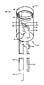
The body section 124 of the doll includes a matrix assembly 132 with
individual LED switch devices 10. In further detail illustrated in FIG. 18,
the matrix
5 assembly
132 includes a printed circuit board 134 upon which the LED switch
devices 10 are mounted in a series of rows 136 and columns 138. As shown, one
LED
switch device 10 from each of the four corners of the matrix is omitted, so in
sum,
there are 77. The heights of the centrally disposed LED switch devices 10 may
be
higher than those peripherally disposed, so as to define a generally spherical
outline.
10 A light
guide 140 that similarly define rows 142 and columns 144 of holes that
correspond to the position of the LED switch devices 10 is mounted on to the
printed
circuit board. It is understood that the light guide 140 directs the light
emission.
Mounted onto the light guide 140 and the matrix of LED switch devices 10 is a
spherical top cover 145 that is contour-matched.
15 Other ways
of constructing the matrix assembly 132 are also known. One low-
cost technique involves mounting and/or etching the respective cathode lead
frame
anvils 16, anode lead frame posts 20, touch sensor lead frame 23,
electroluminescent
semiconductor dies 28, and the touch sensor contacts 39 onto respective sides
and
layers of the printed circuit board 134 in the aforementioned matrix pattern.
20
Thereafter, the electroluminescent semiconductor dies 28 are wire bonded so
that the
respective cathode lead frame anvils 16 and anode lead frame posts 20 are
electrically
connected to the respective cathode contact 30 and anode contact 32 of
electroluminescent semiconductor dies 28. The entire matrix may then be
encapsulated into a single case. The details of this process, as well as
others, will be
25 recognized by those having ordinary skill in the art.
With reference to FIG. 17A and FIG. 17B, one of many possible play patterns
with the interactive doll 122 will now be considered. As particularly shown in
FIG.
17A, the pattern begins with generating a line drawing 148 of a letter, a
number, a
shape, or an object on the LED switch device matrix. For this phase, the
illumination
may be a single color. Thereafter, a loudspeaker can emit a sound that signals
the
player to trace the lines of the pattern with his or her finger, or an
otherwise capacitive
component, in accordance with the sequence as appearing on the matrix.
CA 02825132 2013-07-18
WO 2012/099718
PCT/US2012/020222
26
Referring specifically to FIG. 17B, the user can trace along the lines, and as
the finger traces or covers the specific LED switch devices 10 that were
originally
illuminated, those can change to a different color, as depicted in the changed
LED
switch devices 150. As the user progresses, further audible encouragement is
generated to complete the pattern. Upon successfully completing the tracing of
the
pattern and a detection of the same, the loudspeaker can emit a congratulatory
message and generate various lighting effects therefor. Again, it will be
appreciated
that this sequence has been presented by way of example only and not of
limitation.
Other play patterns are also deemed to be within the purview of those having
ordinary
skill in the art.
The interactive doll 122 is understood to have a similar basic architecture as
described above. More particularly, as shown in the schematic diagrams of FIG.
19A,
FIG. 19B, and FIG. 19C, the interactive doll 122 includes is the
microcontroller or
data processing device 60 with a plurality of input ports 201 and a plurality
of output
ports 202. The output ports 202 are connected to the LED switch devices 10,
which
are arranged as a matrix 214 of 9x9 (-4), or 77 individual ones.
A first set of the touch sensor leads 215a, which are part of each LED switch
device 10 in the matrix 214, are connected to a first touch input controller
58a, while a
second set of touch sensor leads 215b, which are also a part of each LED
switch
device 10 in the matrix 214, are connected to a second touch input controller
58b. As
noted above, the touch input controller 58 detects capacitance changes on the
respective touch sensor contacts 39. Upon detection, a representative signal
is
generated as an output, which is connected to the input ports 201 of the data
processing device 60. In some embodiments however, the touch input controller
58
can be incorporated into the data processing device 60. In further detail, the
data
processing device 60 is programmed with executable instructions that generate
specific outputs to the output ports 202 based on certain inputs, particularly
in
implementing the above-described play pattern.
The audible outputs generated by the interactive doll 122 are through either
the piezoelectric buzzer 208 and/or the loudspeaker 210. One or more motors
206 can
be mechanically linked to the legs 126, arms 128, or the head 130 to animate
the
same. In addition to the foregoing, the interactive doll 122 has additional
functionality
CA 02825132 2013-07-18
WO 2012/099718
PCT/US2012/020222
27
such as data transmission that, for example, is handled by an infrared
transceiver 216,
including a transmitter 216a and a receiver 216b.
The above-described applications of the LED switch device 10 have involved
visible spectrum wavelength emissions therefrom. It need not be limited,
however,
and even emissions of wavelengths in the ultraviolet spectrum are also
contemplated.
With reference to FIG. 20, there is a sanitizing device 280 with another
embodiment
of an ultraviolet LED switch device array 282. As will be recognized,
ultraviolet
radiation can be utilized to sterilize, sanitize, and disinfect a variety of
surfaces, and
the presently contemplated sanitizing device 280 is suitable therefor.
For contextual purposes, one known surface prone to bacteria, viruses, and the
like is a toilet 284. More particularly, the toilet 284 includes a bowl 286 in
which
various waste matter may be deposited. The toilet 284 may include a seat 285
fitted
over the bowl 286 such that a separate contact surface is available for use.
Water held
in a tank 288 is utilized to flush the waste matter in the bowl 286 into the
sewage
system after a flush handle 289 is depressed. Unfortunately, as part of the
flushing
process, miniscule droplets of water containing bacteria and viruses may be
ejected
upwardly and outwardly from the bowl, thereby contaminating the outer surfaces
of
the toilet 284, including the seat 285. As a result, the seat 285 may serve as
a modality
by which contaminants are transferred to its user.
The seat 285 has a flat rim portion 290 with a hole 292 defined within a
center
section thereof. An inner periphery 294 of the flat rim portion 290 has a
countersunk
configuration, within which the ultraviolet LED switch device arrays 282 are
mounted. In further detail, each of the ultraviolet LED switch device arrays
282 may
include one or more LED switch devices 10 that are mounted on a printed
circuit
board 296 that is semi-circular in shape. The LED switch devices 10 therein
are
understood to have one or more electroluminescent semiconductor dies 28 that
are
capable of emitting an ultraviolet wavelength. A ring cover 298 is secured to
the seat
285, and thereby enclosing the ultraviolet LED switch device arrays 282. It is
contemplated that the ring cover 298 is constructed of a transparent epoxy or
poly-
resin, though any other suitably durable material may be utilized. A side
portion 300
includes a control panel 302 as well as a battery compartment 304 that
contains the
energy source for driving the ultraviolet LED switch device arrays 282.
CA 02825132 2013-07-18
WO 2012/099718
PCT/US2012/020222
28
Various automation features may be implemented by the control panel 302.
With a capacitive source touching or coming into proximity with the ring cover
298
and the ultraviolet LED switch device arrays 282, that input may be received
and
processed by the control panel 302, which may then activate the ultraviolet
radiation.
Furthermore, with a loss of the capacitive source (the user has left), the
control panel
may signal a flush handle automation unit 306 to actuate the flush handle 289
without
user intervention. This signaling may be achieved with a pair of complementary
infrared (IR) transceiver modules 308a and 308b associated with a respective
one of
the flush handle automation unit 306 and the control panel 302.
As best illustrated in FIGS. 21A-21C, and as particularly shown in FIG. 21A,
a capacitive source 310 approaches the toilet 284 and the seat 285 thereof. At
this
point, the LED switch devices 10 are not activated to emit an ultraviolet
radiation, and
no inputs to the control panel 302 by way of the capacitive touch sensing has
been
tripped. FIG. 21B shows the capacitive source 310 on the seat 285. Thus, the
touch
sensor contacts of the LED switch devices 10 will exhibit a change in
capacitance and
indicating the same to the control panel 302. In response, the LED switch
devices 10
may be activated to emit the ultraviolet radiation 312, disinfecting the
capacitive
source 310. With the departure of the capacitive source 310 as shown in FIG.
21C, the
touch sensor contacts of the LED switch devices 10 no longer indicates an
input to the
control panel 302, and the ultraviolet emissions may be stopped. At the same
time, the
flush handle automating unit 306 may trigger the flush handle 289 to flush the
toilet
284 and expel any matter that may have been deposited into the bowl 286.
Alternatively, actuating the flush handle 289 may activate a transmission to
the control panel 302 to turn on the LED switch devices 10. As indicated
above, the
flushing action may have deposited contaminants onto the surface of the seat
285.
It will be recognized that while the capacitive source 310 shown in FIGS.
21A-21C is depicted as a pet cat, any other capacitive source such as humans
may be
substituted. Along these lines, while a particular embodiment of the
sanitizing device
280 that utilizes the LED switch device array has been described, it may take
any
other suitable form.
Various applications of the contemplated LED switch device 10 have been
disclosed, including the room lighting dimmer switch 220, the interactive
greeting
card 70, the remote controller 80, the LED display panel 102, the interactive
doll 122,
CA 02825132 2013-07-18
WO 2012/099718
PCT/US2012/020222
29
and the sanitizing device 280. These have been presented by way of example
only,
and it will be appreciated that numerous other applications are possible.
The particulars shown herein are by way of example and for purposes of
illustrative discussion of the embodiments of the present disclosure only and
are
presented in the cause of providing what is believed to be the most useful and
readily
understood description of the principles and conceptual aspects. In this
regard, no
attempt is made to show details of the present invention with more
particularity than
is necessary, the description taken with the drawings making apparent to those
skilled
in the art how the several forms of the present invention may be embodied in
practice.