Note: Descriptions are shown in the official language in which they were submitted.
CA 02825736 2013-08-23
ENHANCED ULTRASOUND IMAGING PROBES USING FLEXURE MODE
PIEZOELECTRIC TRANSDUCERS
FIELD
[0001] This invention relates to methods of generating enhanced flexure mode
signals by piezoelectric transducers and ultrasound imaging probes using the
same.
BACKGROUND
[0002] Ultrasonic transducers are particularly useful for non-invasive as well
as in
vivo medical diagnostic imaging. Conventional ultrasonic transducers are
typically
fabricated from piezoelectric ceramic materials, such as lead zirconate
titanate (PZT)
or PZT-polymer composites, with the transducer material being diced or laser
cut to
form a plurality of individual elements arranged in one-dimensional or two-
dimensional arrays. Acoustic lenses, matching layers, backing layers, and
electrical
interconnects (e.g., flex cable, metal pins/wires) are typically attached to
each
transducer element to form a transducer assembly or probe. The probe is then
connected to control circuitry using a wire harness or cable, where the cable
contains
individual wires to drive and receive signals from each individual element. An
important aim of ongoing research in ultrasonic transducer technology is
increasing
transducer performance and integrability with control circuitry while
decreasing
transducer size, power consumption and signal loss due to the cabling. These
factors
are particularly important for two-dimensional arrays required for three-
dimensional
ultrasound imaging.
[0003] Miniaturization of transducer arrays is particularly important for
catheter-
based 2D array transducers. A significant challenge is the complexity, cost of
manufacture and limited performance of conventional 2D transducer arrays.
Commercial 2D transducer probes are typically limited to arrays with element
pitch of
200 to 300 j_tm and operating frequencies of <5 MHz. The small size of these
elements drastically reduces the element capacitance to <10 pF which produces
high
source impedance and presents significant challenges with electrical impedance
match
to the system electronics. Furthermore, producing forward-looking 2D arrays
for
catheter-based intravascular (IVUS) or intracardiac (ICE) imaging probes has
not
1
CA 02825736 2013-08-23
been achieved commercially. With catheter size of 6 or 7 French or less, the
transducer array should be less than 2 mm in diameter. For adequate
resolution, a
frequency of 10 MHz or greater should be used, which yields a wavelength of
150 vim
in tissue. Because element pitch should be less than the wavelength for
adequate
imaging performance, element pitch of 100 vim or less is desired.
Additionally,
higher frequency operation requires a thinner piezoelectric layer in the
transducers. To
date, conventional transducer arrays have not met these requirements with a
low cost,
manufacturable process and adequate imaging performance.
100041 The production of miniaturized transducers with adequate performance
can
be facilitated by micromachining techniques. The medical devices field, for
example,
has benefited from microelectromechanical systems (MEMS) technology. MEMS
technology allows medical devices or their components to be manufactured with
significant size reduction. Piezoelectric micromachined ultrasonic transducers
(pMUTs) are one such MEMS-based transducer technology. pMUTs generate or
transmit ultrasonic energy through application of AC voltage to a
piezoelectric
material suspended membrane causing it to undergo flexural mode resonance.
This
causes flextensional motion of the membrane to generate acoustic transmit
output
from the device. Received ultrasonic energy is transformed by the pMUT, with
the
ultrasonic energy generating a piezoelectric voltage ("receive signal") due to
flexural
mode resonance vibrations of the microfabricated membrane.
[0005] The benefits of micromachined pMUT devices compared with conventional
ceramic-based transducers include: ease and scalability of manufacture,
especially for
smaller, higher density 2D arrays; simpler integration and interconnection for
2D
arrays; more flexibility in transducer design for wider operating frequency
range;
higher element capacitance for lower source impedance and better match with
electronics. 2D arrays are needed for real-time 3D imaging systems, and
ceramic
transducers are quickly reaching their manufacturability limit for insertion
into
smaller catheter probes (2-3 mm diameter or smaller). Another micromachining
approach is capacitive micromachined ultrasound transducers (cMUTs),
consisting of
surface micromachined membranes on a substrate that are actuated
electrostatically by
applying appropriate DC and AC voltage signals to the membrane electrodes.
However, these devices require multiple elements connected in parallel to
provide
2
CA 02825736 2013-08-23
sufficient acoustic output, thus limiting the performance for 2D arrays with
very small
element size. Sizeable amplification (typically 60 dB) is required in order to
obtain
an ultrasound signal with cMUTs.
[0006] There are functional and structural differences between cMUT and pMUT
devices. Because pMUTs have a higher energy transduction mechanism (i.e., the
piezoelectric layer), the piezoelectric elements generally have higher
ultrasonic power
capability than cMUTs. 2D array pMUT elements with 75 micron width can
generate
acoustic power output of 1 to 5 MPa at a frequency of 8 MHz. Conventional
transducer arrays can generate >1 MPa acoustic pressure, but require much
larger
element size and operate at lower frequency. Typical acoustic output for cMUT
2D
array elements is much less than 1 MPa. Elements in pMUT arrays also have
higher
capacitance (on the order of 100-1,000 pF) than conventional transducer arrays
and
cMUTs, producing lower source impedance and better impedance match to the
cabling and electronics. Conventional transducer arrays elements have
capacitance of
<10 pF, and cMUT elements have capacitance of <1 pF.
[0007] pMUTs typically operate with lower voltages than conventional
transducers
and cMUTs. Depending on the thickness of the ceramic plate, conventional
transducers can require high voltage bipolar signals (>100 V peak-to-peak) to
generate acoustic energy. cMUTs require a large (>100V) DC voltage to control
the
membrane gap distance in addition to an AC signal (typically tens of V peak-to-
peak)
to vibrate the membrane. pMUTs require lower AC voltages (typically 30 V peak-
to-
peak bipolar signal) to acuate the piezoelectric vibration for transmitting
acoustic
energy, and the received ultrasonic energy causes flexural mode resonance
generating
the receive signals without the need for applied voltage.
[0008] Micromachined ultrasound transducers provide miniaturized devices that
may be directly integrated with control circuitry. For example, cMUTs have
been
integrated with control circuitry with through-wafer via connections made by
etching
vias in a silicon wafer, coating the wafer with a thermal silicon dioxide for
insulating
regions and with polysilicon for electrical contacts, and then building up the
cMUT
membrane elements on the top surface of the wafer. Metal pads and solder bumps
may be deposited on the bottom surface of the wafer in order to solder the
cMUT chip
to semiconductor device circuitry.
3
CA 02825736 2013-08-23
100091 One disadvantage of such a cMUT device, however, is that relatively
high
resistivity polysilicon, compared to metals, is used as the conductive
material in the
vias because of processing limitations inherent in the cMUT architecture.
Because of
the already very low signal strength generated by cMUTs in the receive mode,
the
signal to noise ratio may be problematic during operation of the cMUT with
polysilicon vias. Also, the low capacitance of cMUT elements produces high
impedance, and therefore impedance mismatch with the electronics and cabling
are
greater, which contributes to increased signal loss and noise. High resistance
in the
through-wafer vias further exacerbates the high element impedance problem. In
addition, significant resistance in the vias will cause more power consumption
and
heat generation during operation when applying drive signals to cMUTs for
transmit.
10010] Another
disadvantage of the cMUT device with polysilicon through-wafer
interconnects is the processing temperature of forming the thermal silicon
dioxide
insulator and the polysilicon conductor. Processing temperatures for these
steps are
relatively high (600-1000 C), thus creating thermal budget issues for the
rest of the
device. Because of these processing temperatures, the cMUT elements must be
formed after the through-wafer vias are formed, and this sequence creates
difficult
processing issues when trying to perform surface micromachining on a substrate
with
existing etched holes through the wafer.
100111 Conventional transducer arrays may be integrated directly with control
circuitry. However this typically requires solder bumping which is a
relatively high
temperature process (approximately 300 C), and high density integration is
not
feasible due to the large size of the array elements (200 to 300 micron pitch
at a
minimum).
[0012] Thus, pMUT devices offer functional and fabrication advantages over
conventional ultrasound transducers and cMUTs. Intravascular imaging and
interventions are particular areas where miniaturized devices are desirable
and where
MEMS devices are attractive. An example of an application of a MEMS-type
medical device is in imaging devices, such as intravascular ultrasound (IVUS)
and
intracardiac echo (ICE) imaging. IVUS devices, for example, provide real-time
tomographic images of blood vessel cross sections, elucidating the true
morphology
of the lumen and transmural components of atherosclerotic arteries. Such
devices,
4
CA 02825736 2013-08-23
while offering great promise, are amenable to improvement in specific
functionally
dependent performance areas such as receive mode sensitivity.
SUMMARY
100131 In one embodiment, a method of generating an enhanced receive signal
from
a piezoelectric ultrasound transducer is provided. The method comprises
providing a
piezoelectric ultrasound transducer, the piezoelectric ultrasound transducer
comprising a piezoelectric element operable in flexural mode and receiving
acoustic
energy by the piezoelectric element. The acoustic energy is convertible to an
electrical voltage by flexural mode resonance of the piezoelectric element.
The
applied transmit voltage is a sine wave signal that includes an additional
half-cycle of
excitation. The resulting enhanced receive signal generated by the
piezoelectric
transducer is greater than the receive signal generated by the piezoelectric
transducer
for applied transmit voltage without the additional half-cycle excitation.
[0014] In yet another embodiment, a method of generating an enhanced receive
signal from a piezoelectric ultrasound transducer is provided. The method
comprises
providing a piezoelectric ultrasound transducer, the piezoelectric ultrasound
transducer comprising a piezoelectric element operable in flexural mode and
receiving
acoustic energy by the piezoelectric element. The acoustic energy is
convertible to an
electrical voltage by flexural mode resonance of the piezoelectric element. A
DC bias
is applied to the piezoelectric element prior to receiving the acoustic energy
and/or
concurrently with receiving the acoustic energy. An enhanced receive signal is
generated from the piezoelectric transducer by converting the received
acoustic
energy to an electrical voltage by flexural mode resonance of the
piezoelectric
element. The enhanced receive signal generated by the piezoelectric transducer
is
greater than a receive signal generated by the piezoelectric transducer in the
absence
of applying a DC bias.
[0015] In another embodiment, a method of generating an enhanced receive
signal
from a piezoelectric ultrasound transducer is provided. The method comprises
providing a piezoelectric ultrasound transducer (the piezoelectric ultrasound
transducer comprising a piezoelectric element operable in flexural mode) and
applying a sine wave bipolar transmit cycle pulse to the piezoelectric element
to
CA 02825736 2013-08-23
produce an acoustic signal providing an acoustic echo. The sine wave bipolar
transmit cycle pulse has a maximum peak voltage. The acoustic echo is received
by
the piezoelectric element, which is convertible to an electrical voltage by
flexural
mode resonance of the piezoelectric element. A DC bias applied to the
piezoelectric
element prior to receiving the acoustic echo and/or concurrently with
receiving the
acoustic echo and an enhanced receive signal is generated from the
piezoelectric
transducer by converting the received acoustic echo to an electrical voltage
by
flexural mode resonance of the piezoelectric element. The enhanced receive
signal
generated by the piezoelectric transducer is greater than a receive signal
generated by
the piezoelectric transducer in the absence of applying a DC bias.
[0016] In yet another embodiment, an ultrasound imaging catheter is provided.
The catheter comprises a substrate, a plurality of sidewalls defining a
plurality of
openings through the substrate and spaced-apart bottom electrodes on the
substrate.
Each spaced-apart bottom electrode spans one of the plurality of openings and
spaced-
apart piezoelectric elements on each of the bottom electrodes. Conformal
conductive
film on each of the sidewalls of the plurality of openings is in contact with
one or
more of the bottom electrodes and open cavities are maintained in each of the
openings. Means for applying a DC bias to the piezoelectric transducer are
included.
[0017] In yet another embodiment, an ultrasound imaging probe is provided. The
catheter comprises a substrate, a plurality of sidewalls defining a plurality
of openings
partially through the substrate and spaced-apart piezoelectric elements on the
substrate. Each spaced-apart piezoelectric element is positioned over one of
the
plurality of openings. Pairs of spaced-apart bottom electrodes on the
substrate are in
contact with each of the spaced-apart piezoelectric elements. Conformal
conductive
film on each of the sidewalls of the plurality of openings is in electrical
interconnection with one or more of the bottom electrodes and open cavities
are
maintained in each of the openings.
[0018] In yet another embodiment, a method of generating an enhanced receive
signal from a piezoelectric ultrasound transducer is provided. The method
comprises
providing a piezoelectric ultrasound transducer, the piezoelectric ultrasound
transducer comprising a piezoelectric element operable in flexural mode and
having a
ferroelectric coercive voltage. A transmit voltage is applied to the
piezoelectric
6
CA 02825736 2013-08-23
transducer which is above the ferroelectric coercive voltage for the
piezoelectric
element. Acoustic energy is generated by the piezoelectric element providing
an
acoustic echo. An enhanced receive signal is generated from the piezoelectric
transducer by converting the received acoustic echo to an electrical voltage
by
flexural mode resonance of the piezoelectric element. The resulting enhanced
receive
signal generated by the piezoelectric transducer is greater than the receive
signal
generated by the piezoelectric transducer for applied transmit voltage less
than the
coercive voltage.
BRIEF DESCRIPTION OF THE FIGURES
[00191 FIG. I graphically represents an embodiment of the method of enhancing
a
receive signal.
[00201 FIGS. 2-3 illustrate a piezoelectric microfabricated ultrasonic
transducer
device wherein the transducer is attached to a semiconductor device according
to an
embodiment of the invention.
[00211 FIGS. 4-6 illustrate the formation of a piezoelectric microfabricated
ultrasonic transducer device wherein the transducer is attached to a
semiconductor
device according to an embodiment of the invention.
100221 FIG. 7 illustrates a piezoelectric microfabricated ultrasonic
transducer
device wherein the piezoelectric elements are formed on a doped silicon-on-
insulator
substrate.
[00231 FIG. 8 illustrates a piezoelectric microfabricated ultrasonic
transducer
device wherein the transducer is attached to a semiconductor device according
to an
embodiment of the invention.
7
CA 02825736 2013-08-23
[0024] FIGS. 9-15 illustrate an imaging catheter comprising a piezoelectric
microfabricated ultrasonic transducer device according to an embodiment of the
invention.
[0025] FIG. 16 illustrates an imaging probe embodiment.
DETAILED DESCRIPTION
[0026] The embodiments disclosed herein relate to methods of enhancing the
sensitivity of at least one piezoelectric element of an ultrasound flex mode
transducer
by applying a transmit voltage sine wave signal that is above the
ferroelectric coercive
field and/or contains an additional half-wave excitation in the sine wave
signal. The
embodiments further relate to methods of enhancing the sensitivity of a
imaging
device operating with an ultrasound flex mode transducer by applying a DC bias
before and/or with the receive flexural mode resonance of the piezoelectric
element of
the ultrasound flex mode transducer. The embodiments further relate to methods
of
enhancing the sensitivity of a imaging device operating with an ultrasound
flex mode
transducer by applying a DC bias with the receive flexural mode resonance of
at least
one piezoelectric element of the ultrasound flex mode transducer. The
embodiments
herein further relate to improved silicon-on-insulator pMUT (SOI-pMUT)
elements,
their manufacture and use with methods enhancing their sensitivity by applying
a
transmit voltage above the coercive voltage, additional half-wave excitation,
and/or
DC bias with the receive flexural mode resonance of the SOI-pMUT elements. The
embodiments herein further relate to imaging devices comprising flex mode
transducer elements and methods of enhancing their sensitivity by applying a
transmit
voltage above the coercive voltage, additional half-wave excitation, and/or DC
bias
with the receive flexural mode resonance of the flex mode transducer elements.
The
embodiments herein described are generally applicable to medical ultrasound
diagnostic imaging probes comprising flex mode transducers such as pMUTs.
[0027] The terms "microfabricated," "micromachining" and "MEMS" are used
interchangeably and generally refer to methods of manufacturing used in
integrated
circuit (IC) manufacture.
8
CA 02825736 2013-08-23
[0028] The terms "flexural mode," "flexure mode," "flex mode" and
"flextensional
mode" are used interchangeably and generally refer to expansion and
contraction of a
suspended piezoelectric membrane resulting in flex and/or vibration of the
piezoelectric membrane.
[0029] As used herein, the term "flexural mode resonance" refers generally to
excited axisymmetric resonant modes of flex mode transducer elements that
generate
ultrasound acoustic energy of specific frequencies or are caused by receipt of
ultrasound acoustic energy of specific frequencies.
[0030] As used herein, the terms "ferroelectric coercive voltage," -coercive
voltage" and "coercive field" are used interchangably and refer to the voltage
above
which ferroelectric dipole switching of a piezoelectric material occurs.
Coercive field
may be in the range of 1 to 10 V/micron. For example, a piezoelectric membrane
with a thickness of 1 micron typically has a coercive voltage of approximately
3 to 5
V.
[0031] A method for generating enhanced receive signals of a flex mode
transducer
is provided. The method comprises applying a DC bias during and/or prior to
receive
flexural mode resonance of a piezoelectric element. The method is generally
applicable during pulse-echo operation of a flex mode transducer such as a
pMUT.
The method may be adapted to a flex mode transducer using vertically
integrated
pMUT array. The method may further be adapted to catheter-based imaging
devices
comprising a pMUT array and/or a vertically integrated pMUT array to enhance
the
receive signal during pulse-echo operation.
[0032] A method for generating enhanced receive signals of a flex mode
transducer
is provided. The method comprises applying a transmit voltage sine wave signal
that
is above the ferroelectric coercive voltage of the piezoelectric material. The
method
also comprises applying an additional half-wave excitation in the applied
transmit
sine wave signal. The method may be combined with applying a DC bias to the
piezoelectric element prior to receiving the acoustic echo and/or concurrently
with
receiving the acoustic echo. The method is generally applicable to a flex mode
transducer having a thickness-dependent coercive voltage.
[0033] Flexure mode operation presents a unique method for generating acoustic
energy that is significantly different from methods used with conventional
ultrasound
9
CA 02825736 2013-08-23
transducers which typically operate with thickness mode vibration.
Conventional
transducers consist of pre-poled piezoelectric ceramic plates that operate
below the
coercive voltage to generate vibration in the thickness direction of the
plate.
Conventional transducers contain piezoelectric ceramic plates that are
relatively thick
(hundreds of microns thick), thus it is not practical to operate above the
coercive
voltage which would require transmit voltage signals of several hundred volts.
Furthermore, operating above the coercive field would depole the ceramic and
require
repoling at high voltage (hundreds of volts) to achieve sufficient receive
sensitivity.
[0034] pMUT devices may operate by applying a bipolar signal at voltage levels
above the coercive field in order to induce 900 domain switching in the PZT
thin film.
The PZT film is very thin (one to several microns thick), thus operation above
the
coercive voltage can be achieved at relatively low operating voltage levels
(tens of
volts). Internal stress in piezoelectric thin films reduces the ferroelectric
polarization
of the piezoelectric material. The internal stresses in the piezoelectric thin
films
restrict the ferroelectric dipoles, which may result in non-ideal alignment of
the
ferroelectric dipoles in the absence of an applied voltage. By forcing
alignment of the
ferroelectric dipoles, some polarization recovery may be achieved by applying
a
voltage greater than the coercive voltage; however, when the voltage is
removed,
internal stresses reduce the alignment of the ferroelectric dipoles. Thus, pre-
poling
the films does not achieve the maximum dipole alignment, as is the case in
conventional bulk ceramic piezoelectric transducers.
[0035] The methods herein described are in contrast to the typical operation
of
ultrasound transducers using a piezoelectric transducer (conventional or
pMUT),
which transmit with voltage below the ferroelectric coercive voltage.
Transmitting
with voltage above the coercive voltage forces the piezoelectric material to
undergo
ferroelectric 90 domain switching, thus maximizing the flexure of the
membrane
through flextensional motion. The method also describes applying an additional
half-
wave excitation in the sine wave signal to force preferred dipole alignment to
enhance
the pulse-echo receive sensitivity.
[0036] The methods herein described are also in contrast to the typical
operation of
ultrasound transducers using a piezoelectric transducer (conventional or
pMUT),
which receives echo signals in the absence of an applied voltage. The method
for
CA 02825736 2013-08-23
improving the receive signal of a flex mode piezoelectric transducer includes
applying
a DC bias voltage before and/or during receipt of the acoustic signal by the
piezoelectric element. Application of a DC bias before and/or during flexural
mode
resonance of a piezoelectric element of a flex mode transducer increases the
receive
signal (e.g., output current) of the piezoelectric element. When receiving
acoustic
echo signals, the piezoelectric layer in a pMUT is not necessarily poled to
its
maximum extent. One cause of this reduced poling is that the transmit voltage
itself
may depole all or part of the piezoelectric layer. Thus, the application of DC
bias
enhances the dipole alignment and resulting pulse echo receive signal.
[0037] The method of generating enhanced receive signals is discuss below with
reference to a pMUT of particular design but the method is generally
applicable to
any microfabricated piezoelectric elements and piezoelectric ultrasound
elements
operating in flexural mode.
[0038] The method may be performed, by way of example, as follows. Acoustic
energy directed towards a pMUT element is provided. The acoustic energy may be
reflected energy generated from the same piezoelectric element that will
receive the
acoustic energy, reflected energy from a different piezoelectric element of an
array or
reflected energy from another source. By way of example, reflected energy from
the
piezoelectric element as an acoustic echo (pulse-echo) will be discussed.
[0039] In one aspect of the method, a bipolar transmit voltage is applied that
is
above the coercive voltage of the piezoelectric material. This high electric
field level
enhances the ferroelectric 900 domain switching in the piezoelectric layer
which
increases the vibration amplitude of the membrane. This results in higher
acoustic
energy output from the membrane; therefore, higher pulse echo signal is
received due
to the higher transmit energy output. The pulse echo signal can also be
enhanced by
applying an additional half-cycle excitation to the piezoelectric element in
the
transmit signal. Typical transmit voltage pulses contain one, two or three
full-cycle
pulses. Increasing the number of pulses generally increases the transmit
output of the
transducer at the expense of resolution. It is an aspect of this method to
apply an
additional half-cycle excitation, i.e., 1.5, 2.5, or 3.5 cycles, to increase
the sensitivity
of the pMUT element without significantly sacrificing resolution capability
compared
to 1, 2 or 3 cycle pulses. It has been shown that pMUT elements produce higher
pulse
11
CA 02825736 2013-08-23
echo receive signals as a result of applying the additional half-cycle
transmit
excitation compared to full cycle excitation. This is due to enhanced dipole
alignment
in the piezoelectric layer of the pMUT element.
[0040] In another aspect of the method, before the acoustic echo reaches the
transducer, a DC bias may be applied to the piezoelectric element and then
held while
the piezoelectric element is in flexural resonance mode from the received
echo. The
DC bias improves the dipole alignment in the piezoelectric material and thus
increases
the receive signal generated by the membrane. Because the dipole alignment is
improved, higher piezoelectric current is generated as a result of received
acoustic
wave producing mechanical vibration in the membrane. The DC bias can also be
applied to an array of piezoelectric elements, wherein the applied DC bias may
be the
same for all elements or may vary from element to element. pMUT elements can
have some variability in their pulse echo receive characteristics; therefore,
applying a
calibrated DC bias to each element in the array during receive flexure mode
resonance
can also improve the receive signal uniformity across the array for a given
acoustic
pressure to enhance the resulting ultrasound image quality.
[0041] In another aspect of the method, a bipolar transmit voltage may be
applied
to the pMUT to emit acoustic energy. The acoustic energy is reflected from the
target
as an acoustic echo, and returns toward the pMUT. Before the acoustic signal
reaches
the transducer, a DC bias pulse is applied to the transducer prior to the
receive
flexural resonance mode and removed prior to the receive flexural resonance
mode of
the piezoelectric elements. Without being limited by theory, it is generally
believed
that the DC bias pulse temporarily improves the dipole alignment and that upon
removal of the DC bias pulse the dipole alignment does not immediately revert
to its
internally stressed state. Thus, the piezoelectric current output that results
from the
receive flexural resonance mode is increased due to residual polarization from
the
dipole alignment. Piezoelectric output may be lower than in the previously
mentioned
aspect of the method because the dipole alignment is not maximized during
receive
flexural resonance mode. However, this method may obviate the requirement of
additional signal conditioning circuitry. Moreover, as the pulse may be of a
shorter
duration than the previously described aspect of the method wherein the DC
bias is
held while the piezoelectric element is in flexural resonance mode from the
received
12
CA 02825736 2013-08-23
echo, overall power consumption may be reduced. Because the prior transmit
voltage
cycle may depole the piezoelectric material, this method provides enhanced
domain
alignment of a known polarity (in the direction of the DC bias polarity) to
produce an
enhanced receive signal.
[0042] In another aspect of the method, a bipolar transmit voltage is applied
to the
pMUT to emit acoustic energy. The bipolar transmit voltage is stopped at
maximum
peak voltage. The bipolar transmit voltage may be a sine wave transmit cycle
pulse or
other periodic pulse. The acoustic energy is reflected from the target as an
acoustic
echo, and returns toward the pMUT. By stopping the voltage of the transmit
cycle at
peak voltage, retention of dipole alignment may be obtained, which may
increase the
piezoelectric current generated by receive flexural resonance mode of the
piezoelectic
elements from the echo signal. The bipolar transmit voltage may be stopped at
a
voltage between maximum voltage and zero voltage during the transmit cycle.
This
aspect of the method may be combined with other the other aspects of the
method to
enhance the receive signal from the pMUT.
[0043] In another aspect of the method, a bipolar transmit voltage is applied
to the
pMUT to emit acoustic energy. The bipolar transmit voltage is stopped at
maximum
peak voltage. The bipolar transmit voltage may be a sine wave transmit cycle
pulse or
other periodic pulse. The acoustic energy is reflected from the target as an
acoustic
echo, and returns toward the pMUT. Before the acoustic signal reaches the
transducer, a DC bias with opposite sign of that of the transmit peak voltage
is applied
to the transducer and then held during receive flexural resonance mode of the
piezoelectic elements. Without being held by theory, it is believed that this
aspect of
the method forces the ferroelectric dipoles to switch during receive flexural
resonance
mode of the piezoelectic elements from the receive echo. Dipole switching may
generate additional piezoelectric current that may amplify the signal
generated by the
receive echo. The bipolar transmit voltage may be stopped at a voltage between
maximum voltage and zero voltage during the transmit cycle provided that a DC
bias
with opposite sign to that of the stopped transmit cycle voltage is used.
Combinations
of the above aspects are included in the scope of the method.
The timing of the application of the DC bias may be calculated based on the
frequency of the pMUT device and the target depth in the imaging arena. The DC
13
CA 02825736 2013-08-23
bias may be adjusted or chosen to account for internal stresses of the
piezoelectric
membrane layer. The DC bias may be swept from 0 to positive or 0 to negative.
As
the transmit cycle pulse is of the order of nanoseconds, whereas the echo
return is
typically on the order of microseconds, the DC bias duration may be pulsed,
constantly applied, applied in other fashions or applied in combinations with
aspects
of the method described herein such that the receive signal is enhanced.
[0045] Signal conditioning electronic circuitry may be implemented to separate
the
DC bias signal from the generated piezoelectric receive signal and/or to
reduce or
prevent noise in the receive signal. Signal conditioning circuits may be
integrated
directly adjacent to the pMUT substrate or may be integrated in vertically
stacked
ASIC devices. Integration of ASIC devices using through-wafer interconnect
schemes may be as described in co-pending United States Patent Application No.
11/068,776, now issued as U.S. Patent No. 7,449,821. Signal conditioning
circuits
integrated with the pMUT substrate may reduce noise in the receive signal.
Signal
conditioning may be applied to amplify the receive signal. Multiple IC's may
be
stacked with the pMUT using through-wafer interconnect processing such that
signal
conditioning and amplification circuitry is integrated in close proximity with
the
pMUT device for maximizing signal and/or reducing noise which may result from
application of DC bias. Signal conditioning may be performed remotely. Means
for
applying the DC bias to the piezoelectric elements include a pair of
electrically
conductive contacts driven by and in electrical communication with a potential
source. The electrical communication includes wires, flex cabling, and the
like.
Potential sources include a battery, AC or source/drain and the like. The
electrically
conductive contacts, in communication with a potential source, may be
connected to
the piezoelectric elements such that an active electrical circuit is created
and
controlled. Such electrically conductive contacts may be in series or parallel
with the
elements. Means and equivalents thereof include additional circuitry and/or
electronic components designed to control the DC bias concurrently with
transmit and
receiving signals as is within the ordinary skill of the skilled artisan, such
as with
filtering or low noise amplifiers.
[0046] Application of the above method of generating enhanced receive signal
may
be integrated with the pMUT and silicon-on-insulator (SOI) substrate pMUT
devices
14
CA 02825736 2013-08-23
(SOI-pMUT) and/or vertically stacked ASIC-pMUT devices as disclosed in co-
pending application U.S. Patent Application No. 11/068,776, now issued as U.S.
Patent No. 7,449,821, for example, as described below.
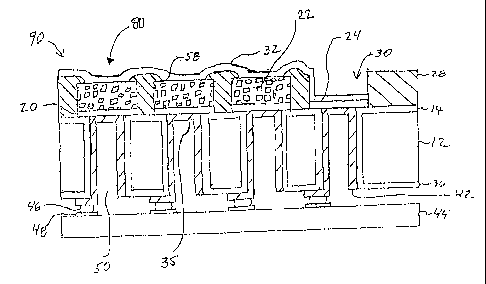
[0047] Referring to FIG. 2, a pMUT device structure 80 is shown connected to a
semiconductor device 44 to form a vertically integrated pMUT device 90. By way
of
example, the connection is made through solder bumps 46 connecting the
conformal
conductive layer 42 to solder pads 48 on the semiconductor device 44.
100481 Top electrode 32 and bottom electrode 20 sandwich piezoelectric array
elements 22 separated by second dielectric 28 which overlaps edges 58 of
elements
22. Bottom electrodes 20 are isolated by first dielectric layer 14 which is
etched away
during subsequent formation of air-backed cavities 50 in back side of
substrate 12.
Air back cavities 50 have sidewalls coated with conformal insulating film 36
and
conformal conductive film 42 providing thru-wafer via interconnect of the
semiconductor device 44 with the piezoelectric array elements 22. The
patterned
through-wafer interconnects 42 provide direct electrical connection from the
piezoelectric membranes 35 to the semiconductor device 44 and ground pad 24 in
opening 30. The air-backed cavities 50 provide optimum acoustic performance.
The
air-backed cavity 50 allows greater vibration in the piezoelectric membrane 35
with
minimal acoustic leakage compared to surface microfabricated MUTs.
[0049] Vertically integrated pMUT device 90 including second dielectric film
28
on the top edges of the patterned piezoelectric layer 58 provides improved
electrical
isolation of the two electrodes 32, 20 connected to the piezoelectric elements
22. This
embodiment helps account for any photolithography misalignment which could
inadvertently cause a gap between the polymer dielectric 28 and piezoelectric
element
22 edges causing the top electrode 32 to short to the bottom electrode 20. The
second
dielectric film 28 also eliminates the need for any planarization processes
that might
be required in other embodiments. This embodiment further provides a method of
forming a size or shape of the top electrode 32 that is different from the
size and
shape of the patterned piezoelectric elements 22. If thick enough (on the
order of the
piezoelectric thickness), the second dielectric film 28 with much lower
dielectric
constant than the piezoelectric elements 22 causes the voltage applied to the
pMUT
90 device to primarily drop only across the dielectric, thus electrically
isolating the
CA 02825736 2013-08-23
portion of the piezoelectric layer 58 that is covered with the dielectric. The
effective
shape of the piezoelectric element 22 with regard to the applied voltage is
only the
portion of the piezoelectric elements 22 that is not covered with the
dielectric. For
example, if it is desired only to electrically activate 50% of the total
piezoelectric
geometrical area, then polymer dielectric 28 may physically cover and
electrically
isolate the remaining 50% of the piezoelectric area and prevent it from being
activated. Also, if a complex electrode pattern is desired such as an
interdigitated
structure, a polymer dielectric may be used for the second dielectric layer 28
and may
be patterned to provide the interdigitated structure. This is important for
certain
embodiments wherein the top electrode 32 is a continuous ground electrode
across the
entire pMUT array. Simpler processing is provided by creating the electrically
active
area by patterning the polymer dielectric 28, thus the active area assumes the
shape of
the top electrode area contacting the piezoelectric element 22, rather than
patterning
the bottom electrode 20 and a piezoelectric film.
[0050] Vibrational energy from surface microfabricated membranes may be
dissipated into the bulk silicon substrate which resides directly below the
membrane
thus limiting the ultrasonic transmit output and receive sensitivity. The air
backed
cavity 50 of the present invention reduces or eliminates this energy
dissipation since
the vibrating membrane 35 does not reside directly on or over the bulk
substrate 12.
[0051] The semiconductor device 44 may be any semiconductor device known in
the art, including a wide variety of electronic devices, such as flip-chip
package
assemblies, transistors, capacitors, microprocessors, random access memories,
multiplexers, voltage/current amplifiers, high voltage drivers, etc. In
general,
semiconductor devices refer to any electrical device comprising
semiconductors. By
way of example, the semiconductor device 44 is a complementary metal oxide
semiconductor chip (CMOS) chip.
[0052] Because each piezoelectric element 22 is electrically isolated from
adjacent
piezoelectric elements 22, the individual elements may be separately driven in
the
transducer transmit mode. Additionally, receive signals may be measured from
each
piezoelectric membrane independently by the semiconductor device 44. Receive
signals may be enhanced by the method of applying a DC bias for each or every
16
CA 02825736 2013-08-23
piezoelectric element independently by the semiconductor device 44. Receive
signal
conditioning and DC bias circuitry may be integrated with semiconductor device
44.
[0053] An advantage of the formation of the through-wafer interconnects 42 is
that
separate wires, flex cable, etc., are not required to carry electrical
transmit and receive
signals between the membranes 35 and semiconductor device 44, as electrical
connection is provided directly by the interconnects 42. This reduces the
number of
wires and size of the cabling required to connect the ultrasonic probe to a
control unit.
Furthermore, the shorter physical length of the through-wafer interconnects 42
(<1 mm) compared with conventional cable or wire harnesses (length on the
order of
meters) provides connections with lower resistance and shorter signal path
which
minimizes loss of the transducer receive signal and lowers the power required
to drive
the transducers for transmit.
[0054] The use of metal interconnects 42 and electrodes 20, 32 may provide a
piezoelectric device with higher electrical conductivity and higher signal-to-
noise
ratio than devices using polysilicon interconnects and electrodes. In
addition, the use
of low temperature processes of depositing the conformal insulating layer 36
and
conformal conductor 42 reduces the thermal budget of the device processing,
thus
limiting the damaging effects of excessive exposure to heat. This also allows
the
piezoelectric elements 22 to be formed before etching the through-wafer via
holes 50
in the substrate, thus simplifying the overall processing.
[0055] When a pMUT device structure is attached directly to a semiconductor
device substrate, there may be observed some reverberation of the pMUT
elements as
acoustic energy is reflected off of the semiconductor device substrate and
directed
back toward the piezoelectric membrane. The reverberation causes noise in the
pMUT signal and reduces ultrasound image quality. Also the acoustic energy
could
affect semiconductor device operation by introducing noise in the circuit. By
way of
example, using an acoustic dampening polymer coating on the contacting surface
of
the semiconductor device, or at the base of the air-backed cavity of the pMUT
device,
acoustic energy reflected from the piezoelectric membrane may be attenuated.
The
acoustic dampening polymer layer preferably has a lower acoustic impedance and
reflects less ultrasonic energy than a bare silicon surface of the
semiconductor device
with high acoustic impedance. By way of example, the acoustic dampening
polymer
17
CA 02825736 2013-08-23
layer may be also function as an adhesive for attachment of the pMUT device
structure to a semiconductor device.
[0056] The thickness of piezoelectric elements 22 of the pMUT device may range
from about 0.5 pm to about 100 gm. By way of example, the thickness of the
piezoelectric elements 22 ranges from about 1 pm to about 10 rim.
[0057] The width or diameter of the piezoelectric elements 22 may range from
about 10 pm to about 500 pm with center-to-center spacing from about 15 tim to
about 1000 tn. By way of example, the width or diameter of the piezoelectric
elements 22 may range from about 50 jim to about 300 pm with center-to-center
spacing from about 75 gm to 450 gm for ultrasonic operation in the range of 1
to 20
MHz. Smaller elements of less than 50 gm may be patterned for higher frequency
operation of >20 MHz. By way of example, multiple elements may be electrically
connected together to provide higher ultrasonic energy output while still
maintaining
the high frequency of operation.
[0058] The thickness of the first dielectric film 14 may range from about 10
nm to
about 10 gm. By way of example, the thickness of the conformal insulating film
36
ranges from about 10 nm to about 10 gm. The thickness of the bottom electrode
20,
top electrode 32, and conformal conductive layer 42 ranges from about 20 nm to
about 25 pm. The depth of the open cavity 50 may be range from about 10 pm to
several millimeters.
[0059] In one embodiment, a pMUT device structure 10 is connected to the
semiconductor device 44 through metal contacts 54 formed in the epoxy layer 56
on
the semiconductor device 44 forming vertically integrated pMUT device 70, as
illustrated in FIG. 3. The epoxy layer 56, in addition to functioning as an
acoustic
energy attenuator, may also function as an adhesive for adhering the pMUT
device
structure 10 to the semiconductor device 44. The epoxy layer 56 may be
patterned
using photolithographic and/or etching techniques, and metal contacts may be
deposited by electroplating, sputtering, electron beam (e-beam) evaporation,
CVD, or
other deposition methods.
In certain embodiments, application of the above method of enhancing receive
signal
may be integrated with the pMUT fabricated with a silicon-on-insulator (SOI)
substrate as the substrate as previously described in co-pending U.S. Patent
18
CA 02825736 2013-08-23
Application No. 11/068,776, now issued as U.S. Patent No. 7,449,821, as shown
in
FIGS. 4-6, for example, as well as an improved SOI-pMUT device as described
below
with reference to FIG. 7.
[0061] As shown in FIG. 4, a substrate 12, such as a silicon wafer, is
provided with a
thin silicon layer 62 overlying a buried silicon dioxide layer 64 formed on
the substrate
12. A first dielectric film 14 is formed overlying the silicon layer 62 and a
bottom
electrode layer 16 is formed overlying the first dielectric film. A layer of
piezoelectric
material 18 is formed overlying the bottom electrode layer 16 to pro\ ide a
SOI pMUT
device structure 100. At least one advantage of using the SOI substrate
includes better
control of the deep reactive ion etching (DRIE) using the buried oxide as the
silicon
substrate etch stop. The SOI also provides better control of the pMUT membrane
35
thickness for better control and uniformity of the resonance frequencies of
the
individual elements in an array, as the membrane thickness is defined by the
thickness
of the thin silicon layer of the SOI substrate 62. According to certain
embodiments, the
thin silicon layer 62 has thickness of about 200 nm to 50 pm, and the buried
oxide layer
64 has thickness of about 200 nm to 1 m. In other embodiments of the present
invention, the thin silicon layer 62 has thickness of about 2 p,m to 20 pm,
and the buried
oxide layer 64 has thickness of about 500 nm to 1 pm.
[0062] With reference to FIG. 5, the layer of piezoelectric material 18,
bottom
electrode layer 16, first dielectric film 14, silicon layer 62, and buried
silicon oxide
layer 64 are subsequently etched to provide separate piezoelectric elements 22
and a
ground pad 24, and to expose the front side 13 of the substrate 12. The
piezoelectric 18
and bottom electrode 16 layers are etched to form the pMUT element shape 22
separated by openings 68. The first dielectric 14, thin silicon 62, and buried
oxide 64
layers are further etched to form spaced-apart vias 69 exposing the substrate
12. A
conductive film 66 is deposited in the spaced-apart vias 69, as illustrated in
FIG. 5, to
provide electrical connection between the bottom electrode 20 and the through-
wafer
interconnects to be subsequently formed. Patterning of the pMUT device
structure 100
may be done using conventional photolithographic and etching techniques. By
way of
example, the conductive film 66 may be of metals such as Cr/Au, Ti/Au, Ti/Pt,
Au, Ag,
Cu, Ni, Al, Pt, In, Ir, m02, Ru 02, In203:Sn02 (ITO) and (La, Sr)Co03 (LSCO),
with
respect to the bottom electrode 20, top electrode 32, and conformal conductive
layer 42.
19
CA 02825736 2013-08-23
[0063] The SOI-pMUT device structure 100 is further processed to form the
second
dielectric film 28 and top electrode 32. Through-wafer vias 34 are formed, for
example by deep reactive ion etching (DRIE). The conformal insulating layer
36, and
conformal conductive film 42, are formed in the through-wafer vias as
illustrated in
FIG. 6. Electrical contact between the conductive film 66 and the conformal
conductive film 42 provide a through-wafer interconnect. The SOI-pMUT device
structure 100 is connected to a semiconductor device 44, such as through
solder
bumps 46, as shown in FIG. 6, to form a vertically integrated pMUT device 110.
In
other embodiments, the semiconductor device 44 may be electrically connected
to the
conformal conductive film 42 through metal contacts formed in an epoxy layer
deposited on the surface of the semiconductor device which attaches the pMUT
device to the semiconductor device, as previously described.
[0064] Application of the above method of enhancing receive signal may be
integrated with an improved silicon-on-insulator (SOI) substrate pMUT device
and/or
vertically stacked ASIC devices as follows.
[0065] Previously described pMUT devices with air-backed cavities provided the
bottom electrode in direct contact with the conformal metal layer in the air-
backed
cavity, or a metallized plug through an SO1 layer to contact the plug metal to
the
conformal metal layer. The fabrication of an improved SOI air-backed cavity
pMUT
provides Si02 or device silicon structural layers as the membrane which may
provide
for more accurately targeting a specific resonance frequency, since frequency
is
dependent on membrane thickness and provides for direct electrical contact
with the
piezoelectric element through the air-back cavity. Thus, a heavily doped,
electrically
conductive, device silicon layer in the SOI substrate providing electrical
interconnection between the bottom electrode and conformal metal layer through
the
air-backed cavity was envisaged. A pMUT of this embodiment is exemplified
below
with reference to FIG. 7.
[0066] SOI substrate 120 with a heavily doped (<0.1 ohm-cm resistivity) device
silicon layer 162 is provided on the buried oxide layer 164 on the front
surface of the
substrate 120. A Si02 passivation layer 175 is thermally grown on the surface
of
device silicon layer 162 to prevent diffusion of bottom electrode layer 116
into doped
device silicon layer 162 in subsequent processing steps. Si02 layer 175 is
patterned
CA 02825736 2013-08-23
by photolithography and etching. Bottom electrode layer 116 may be deposited
by
sputtering or electron beam evaporation and may be Pt or Pt/Ti. Ti may be used
for
adhesion of the Pt to Si02 layer. Preferably, the metal of bottom electrode
116 is able
to withstand piezoelectric material anneal temperatures. The bottom electrode
may be
patterned by photolithography and etch or liftoff processing. The bottom
electrode
may be as described above.
[0067] Patterned piezoelectric elements 22 may be formed by depositing
piezoelectric material by spin coating, sputtering, laser ablation or CVD, and
annealing, typically at a temperature of 700 C. Patterning may be performed,
for
example, by photolithography and etching. Patterned piezoelectric elements 22
are
etched such that the piezoelectric layer width is less than the width of the
bottom
electrode. This provides access to the bottom electrode such that the
subsequent
metal connector may be formed.
[0068] Metal connector layer 180 is deposited and patterned by
photolithography
and etch or liftoff processing. The metal connector layer 180 may be Ti/Pt,
Ti/Au, or
other metal as described above. Ti may be used for adhesion of Pt or Au to
heavily
doped device silicon layer 162. Metal connector layer 180 provides electrical
contact
between the bottom electrode 116 and heavily doped device silicon layer 162.
[0069] Device silicon layer 162 is patterned by photolithography and etched to
provide an isolation trench 130 adjacent to each piezoelectric element 22
providing
electrical isolation of the piezoelectric elements 22 within an array with
respect to
each other. Isolation trench 130 is etched to the buried Si02 layer 164.
[0070] Polymer dielectric layer 128 is deposited on top of piezoelectric
elements 22
including trenches 130 and patterned by spin coating, photolithography and
etching.
Photoimageable polymeric dielectric materials may be used for the polymer
dielectric
layer 128. Polymer dielectric material may be polyimide, parylene,
polydimethylsiloxane (PDMS), polytetrafluoroethylene (PTFE),
polybenzocyclobutene (BCB) or other suitable polymers.
[0071] Metal ground plane layer 132 is deposited, for example by electron beam
evaporation, sputtering or electroplating. Ti/Au or Ti/Cu may be used for
metal =
ground plane layer 132.
21
CA 02825736 2013-08-23
100721 Polymer passivation layer 190 is deposited, for example, by vapor
deposition or spin coating. Polymer passivation layer 190 provides electrical
and
chemical insulation from fluid that may come in contact with the device
surface
during use (e.g., blood, water, silicone gel), and may also serves as an
acoustic
matching layer providing a lower acoustic impedance layer between the
transducer
face and the fluid.
[0073] Etching of back side of silicon substrate 120 provides air-backed
cavities
150. Ground vias 131 are etched providing connection of the conformal
conductor
143 to the doped silicon layer 162 and to the metal ground plane layer 132.
Etching
may be by deep reactive ion etching (DRIE).
100741 Conformal insulator layer 136 is deposited on sidewalls 137 and base
125 of
the air-backed cavities 150 as well as on back surface 111 of substrate 120.
Conformal insulator layer 136 of base 125 is etched if a via is required, for
example,
for interconnection. Conformal insulator layer 136 may be polymer, oxide or
nitride
material.
[0075] Conformal metal layer 142 is deposited inside of air-backed cavity 150
including sidewalls 137 and base 125 and back surface 111 of substrate 120.
Conformal metal layer 142 may be sputtered, e-beam evaporated, or CVD
deposited.
100761 Conformal metal layer 142 is patterned on back surface 111 of substrate
120
by photolithography and etched to electrically isolate piezoelectric elements
22 and
ground via 131 from one another. Conformal metal layer 142 also provides
interconnect pad 143 for electrical connection of the pMUT device to an IC
device.
Thus, electric contact from the piezoelectric element through the air-backed
cavity of
a SOI-pMUT device is provided with possible processing advantages and
performance benefits.
100771 In certain embodiments, application of the above method of generating
an
enhanced receive signal may be carried out using the pMUT devices or pMUT
devices fabricated with a SOI substrate bonded to ASIC devices. Such
vertically
integrated devices include those previously described in co-pending U.S.
Patent
Application No. 11/068,776, now issued as U.S. Patent No. 7,449,821. An
improved
bonding structure for providing compactness of the pMUT-ASIC stack for
application
in imaging probes such as catheters of small diameter, for example, is as
follows.
22
CA 02825736 2013-08-23
[0078] A pMUT substrate may be mechanically attached and electrically
connected to an IC substrate such as an ASIC device, for example, as shown in
FIG.
3. Connection of the pMUT to the IC substrate may be by epoxy bonding or by
solder
bump bonding. IC substrates bonded by solder bumps typically have thicknesses
of
multiple millimeters, depending on the number of IC layers. It is desirable to
further
reduce overall thickness and increase compactness of the pMUT-IC assembly. A
preferred method for bonding of the pMUT and IC substrates is epoxy bonding.
Epoxy bonding may provide greater physical compactness and lower overall
thickness
in the assembled device and may provide lower temperature processing steps
compared to solder bumping.
[0079] An example of an improved epoxy bonded pMUT-IC stack 220 is shown in
FIG. 8. Epoxy interconnect layer 256 is deposited on surface of IC substrate
320
providing bonding with pMUT device 10. A conformal dielectric 52 is deposited
to
isolate the through-wafer electrical interconnects 230 and IC substrate 320.
Through-
wafer interconnects 230 may be etched in the IC layer and through the epoxy
interconnect layer 256 to expose metal interconnection pad 242 on the back
side of
the pMUT device 10. The etching may be by DRIE, and the through-wafer
interconnects 230 may be metallized using CVD and/or electroplating. A second
IC
substrate 420 may be subsequently bonded with vias formed similarly and
electrical
connections formed similarly. Electrical leads 301 (e.g., wires, flex cables,
etc.) may
be attached to the back side or one or more IC substrates to provide
electrical
connection from the pMUT-IC stack to the system electronics or catheter
electrical
connector.
[0080] The IC substrates may be thinned by chemical-mechanical polishing
(CMP).
Thinning of the IC silicon substrates using CMP may significantly reduce the
overall
thickness of the stack, and may provide a thickness of less than 1 mm for the
entire
stack. CMP may also provide for via etches that may be shallower and for via
sizes
that may be smaller, as aspect ratios of typically no more than 10:1 may be
formed
using conventional silicon etch and CVD metal via forming processes. The pMUT
substrate may also be thinned by CMP or other process prior to forming air
backed
cavities 250.
23
CA 02825736 2013-08-23
100811 Solder bump or wire bond stacking (e.g., system-on-chip or system-on-
package) requires additional lateral area due to die handling and wirebonding
constraints. The epoxy bonding method requires no additional lateral area, as
fiducials may be formed on the back sides of the IC substrates, and alignment
and
bonding of two substrates may be formed by precision aligner-bonder equipment.
Thus, when vias are etched in the silicon substrates, the vias are pre-aligned
to the
interconnect pads of the previous substrate. Therefore, the entire pMUT-IC
stack 220
need be no larger in lateral area than the pMUT array itself.
[00821 pMUTs formed with through-wafer interconnects combined with control
circuitry as described above thereby forming a transducer device may be
further
assembled into a housing assembly including external cabling to form an
ultrasonic
probe, such as an ultrasound imaging probe. The integration of pMUTs with
control
circuitry may significantly reduce the cabling required in the ultrasonic
probe. The
ultrasonic probe may also include various acoustic lens materials, matching
layers,
backing layers, and dematching layers. The housing assembly may form an
ultrasonic
probe for external ultrasound imaging, or a catheter probe for in vivo
imaging. The
shape of the ultrasound catheter probe housing may be of any shape such as
rectangular, substantially circular or completely circular. The housing of the
ultrasound catheter probe may be made from any suitable material such as
metal, non-
metal, inert plastic or like resinous material. For example, the housing may
include a
biocompatible material comprised of a polyolefin, thermoplastic, thermoplastic
elastomer, thermoset or engineering thermoplastic or combinations, copolymers
or
blends thereof.
100831 Methods for generating enhanced receive signal of an ultrasound
catheter
probe are provided. The methods comprise providing an ultrasound catheter
probe
comprising a pMUT or a pMUT integrated with an application-specific integrated
circuit (ASIC) device assembly and incorporating the assembly in an imaging
device
and supplying a DC bias during receive flexural resonance mode of the pMUT for
generating an enhanced receive signal from the pMUT. Such embodiments are
further described with reference to FIGS. 9-15.
100841 pMUT device 90 may be bonded to a flex cable 507 or other flexible wire
connection providing imaging catheter devices 500, 600 as shown in FIGS. 9-10.
24
CA 02825736 2013-08-23
This may be done by solder bump bonding, epoxy (conductive epoxy or
combination
of conductive and nonconductive epoxy), z-axis elastomeric interconnects, or
other
interconnection techniques used for catheter-based ultrasound transducers.
[0085] Referring to FIG. 9, forward viewing imaging catheter device 500
includes
associated pMUT 90 integrated with flex cable 507 for imaging through an
acoustic
window 540. Side viewing catheter 600 includes associated pMUT 90 integrated
with
flex cable 507 and acoustic window 640, as depicted in FIG. 10. Catheters 500
and
600 include acoustically matching material 550, 650, respectively, directly in
contact
with pMUT 90. Acoustic matching material 550, 650 may be a low elastic modulus
polymer, water or silicone gel.
[0086] Catheter 700 includes pMUT 90 with vertically integrated ASIC devices
720, 730 which may be multiplexer, amplifier or signal conditioning ASIC
devices or
combinations thereof. Additional ASIC devices may also be included such as
high
voltage drivers, beam formers or timing circuitry. Acoustic window 740 may
include
acoustically matching material 750 directly in contact with pMUT 90.
[0087] Imaging catheter devices 500, 600, 700 may have an outside diameter in
the
range of 3 French to 6 French (1-2 mm), but may also be as large as 12 French
(i.e.
4 mm) for certain applications. Such a device may be able to access small
coronary
arteries. It is desired that minimal number of electrical wires be assembled
in small
catheter probes, thus miniature integrated circuit switches (e.g.
multiplexers) can
provide for reduction of electrical wires inside of the catheter. The housing
509 of
imaging catheter device 500, 600, 700 may be highly flexible and may be
advanced
on a guide-wire, for example, in the epicardial coronary arteries.
[0088] Signal wires or flex cable leads can be connected directly with the
through-
wafer interconnects on the back side of the pMUT substrate as shown in FIG. 9.
The
wires or flex cable can be routed through the catheter body and connected
through the
1/0 connector at the back end of the catheter to external control circuitry.
However, it
would be beneficial to reduce the number of electrical leads contained in the
catheter
sheath in order to allow greatest mechanical flexibility for steering/guiding
the
catheter through vessels. For example, a 7F (3 mm diameter) catheter, a 20x20
element pMUT array may be used to produce high quality images. In this case, a
minimum of 1 wire per element totaling at least 400 wires would be required to
drive
CA 02825736 2013-08-23
the pMUT array at the tip of the catheter. This would leave little room for a
guide
wire to direct the catheter movement and little flexibility to bend the
catheter.
[0089] Thus, in order to reduce the number of signal leads and signal noise in
the
catheter, the pMUT device may be integrated with control circuitry in the
catheter tip.
For example, as shown in FIG. 8, the readout function may be directly
integrated with
the transducer array using through-wafer interconnects. An amplifier ASIC may
be
bonded to the pMUT substrate and connected to the through-wafer interconnects
of
each pMUT element such that the ultrasonic signal received by each pMUT
element
is amplified independently to maximize signal-to-noise ratio. This direct
integration
may also greatly reduce the electrical lead length between the pMUT element
and the
amplifier to further reduce signal noise. By integrating a second multiplexing
ASIC,
the signal received by each transducer and sent to each amplifier may be
multiplexed
through a reduced number of signal wires to the I/0 connector at the back end
of the
catheter. Thus, less wires are required within the catheter sheath. The speed
of the
multiplexing will determine the reduced number of signal wires that may be
achieved.
Reducing the number of leads also reduces the crosstalk between elements.
[0090] Through-wafer interconnects may be formed by etching the silicon
substrate
of the ASIC, coating the etched holes with conformal dielectric and metal
layers, and
plating metal to produce filled conductive vias, as described above. Multiple
circuits
may be stacked by epoxy bonding with aligned through-wafer interconnects.
In addition to integrating the receive function of the transducer array, the
drive or
transmit function may be integrated with the pMUT substrate in a similar
fashion.
High voltage drivers included in the ASIC stack may be used to generate the
necessary to drive the transducer elements, and multiplexing circuitry can be
used to
address individual pMUT elements. Thus, 2D phased array operation may be
achieved by multiplexing the drive signal with appropriate timing. At least
one
advantage of directly integrating the transmit function is that high voltage
is generated
directly adjacent to the pMUT array. Highvoltage signals transmitted through
the
body of the catheter would be reduced or eliminated, thus improving the
electrical
safety of the catheter. Low voltage signals (3-5V) may be sent from the I/0
connector
to the integrated multiplexing and high voltage driver circuitry, and the
drivers
26
CA 02825736 2013-08-23
generate the higher transmit voltage through charge pumps and/or inductive
transformers.
[0092] Other circuitry may be integrated in the ASIC stack such as timing
and/or
beam forming circuitry to control the transmit/receive signals and produce the
ultrasound imaging signal from the raw pMUT signals. This integration may
reduce
the amount and size of electronics required in the external control unit,
enabling a
smaller, hand-held ultrasound imaging system or portable catheter-based
ultrasound
imaging system.
[0093] It is envisioned that the embodiments herein described are applicable
to
forward or side viewing catheters operating with 2D, 1.5D or 1D arrays.
[0094] Referring now to FIGS. 12-15, pMUT device 990 of catheters 800, 900 is
constructed to provide for a manipulative member 807 or optical fiber 907. The
manipulative member may be a catheter guide wire. The manipulative member may
include a surgical instrument such as a scalpel, needle or syringe. The
manipulative
member may be remotely controlled through the catheter or housing assembly.
Manipulative member 807 or optical fiber 907 is positioned in bore hole 870,
970,
respectively. The manipulative means may be controlled externally. Bore 970
may
include seal 880 to secure manipulative member 807 and to prevent seepage of
fluid
into the catheter. Manipulative member 807 may also be movable or retractable
with
respect to bore 870 and seal 880. Optical fiber 907 can be affixed directly to
sidewalls of bore 970 and sealed with epoxy or other seal or adhesive. Such
manipulative means such as guide wire, surgical tool or optical fiber may be
adapted
,
to stacked pMUT-IC devices in a similar manner. Bore holes 870, 970 may be
provided during processing of the pMUT or pMUT-IC stack using etching
processes,
for example DRIE. The bore hole is cooperatively aligned with a suitable sized
opening 513 in the distal end of the catheter. An internal passage 517 through
the
interior of the catheter housing communicable with the bore and opening 513
provides
for the insertion and manipulation of the manipulative member.
[0095] The imaging catheter devices 600, 700, 800, 900 further comprise a
steering
mechanism 505 coupled to the proximal portion of the conduit. By way of
example,
at least one steering mechanism is disclosed in U.S. Patent No. 6,464,645. A
controller for the ultrasonic transducer assembly
27
CA 02825736 2013-08-23
may also be provided that is contoured to a human hand to provide a
comfortable and
efficient one-handed operation of controls on the controller.
[0096] The catheter probes and pMUT transducer elements herein disclosed may
be
adapted to sterilization as is conventionally performed for medical devices.
The
pMUT devices and methods of generating enhanced receive signal described
herein
may be used for procedures such as real time, three-dimensional intracardiac
or
intravascular imaging, imaging for minimally invasive or robotic surgeries,
catheter-
based imaging, portable ultrasound probes, and miniature hydrophones. The
pMUTs
may optimized for operation in the frequency range of about 1-20 MHz.
[0097] The ultrasound catheter probe herein disclosed may be particularly
suited
for IVUS and ICE of coronary thrombosis of a coronary artery. Such treatment
may
be necessary to treat or possibly reduce coronary artery disease,
atherosclerosis or
other vascular related disorders.
[0098] The methods and embodiments herein described may be used to produce an
external ultrasound probe with enhanced sensitivity. Thus, the vertically
integrated
pMUT device may also be adapted for use in external ultrasound probes, for
example
for cardiology, obstetrics, vascular, or urological imaging. Thus, as shown in
FIG. 16,
forward viewing imaging probe device 1000 includes associated pMUT 90
integrated
with flex cable 1507 for imaging through an acoustic window 1740. Probe 1000
includes vertically integrated ASIC devices 1720, 1730, which may be
multiplexer,
amplifier or signal conditioning ASIC devices or combinations thereof with
pMUT
90. Additional ASIC devices may also be included such as high voltage drivers,
beam
formers or timing circuitry. Acoustic window 1740 may include acoustically
=
matching material 1750 directly in contact with pMUT 90.
[0099] pMUT arrays with 1D, 1.5D or 2D geometries can be fabricated and
integrated with ASIC devices to provide electronic signal processing in the
handle of
the transducer probe. The pMUT-IC stack can be mounted in an external probe
housing with an acoustic matching layer consisting of a low elastic modulus
polymer,
water, or silicone gel between the pMUT face and the housing wall. The pMUT-IC
stack may be mounted to flex cable, ribbon cable, or standard signal wires for
interface to the imaging system electronics.
28
CA 02825736 2013-08-23
1001001 Conventional ultrasound transducer arrays with integrated electronics
for
external ultrasound probes require costly, complex manufacturing techniques.
An
external pMUT-based probe may provide a lower cost, more manufacturable
product
due to semiconductor batch fabrication and integration techniques.
EXAMPLE
[00101] The method of generating enhanced receive signals from an ultrasound
piezoelectric transducer are further described with reference to the following
example.
[00102] A single pMUT element was subjected to an DC bias from -20 Vdc to +20
Vdc. An acoustic signal provided by a separate piston transducer was aimed at
the
pMUT element. Signal received by the pMUT element was measured as a function
of
applied DC bias. Referring to FIG. 1, a graph depicting receive signal in
millivolts
peak-to-peak verses bias voltage is shown. The data in FIG. 1 represents the
output
response of the pMUT element for different levels of DC bias voltage. The DC
bias
voltage was varied from 0 V to +20V, back to OV, then from OV to -20V. Receive
signal (mV) was recorded at each DC bias increment. FIG.1 depicts the optimum
DC
bias voltages for increasing receive sensitivity with respect to the coercive
field level
in this particular piezoelectric thin film. When the DC bias was near the
coercive
voltage (approximately -5V) of the piezoelectric film in the pMUT element,
receive
sensitivity decreased. As the applied voltage increased the output signal of
the pMUT
element increased. Thus, the method of applying a DC bias to generate enhanced
receive signal of a pMUT element was demonstrated. Optimization of the
enhancement in receive signal may be obtained by adjusting the DC bias while
monitoring the receive signal from a piezoelectric membrane of known
thickness.
29