Note: Descriptions are shown in the official language in which they were submitted.
CA 02827959 2013-09-20
APPARATUS AND METHOD FOR ELECTRICAL STABILITY COMPENSATION
FIELD
The present disclosure relates generally to electrical stability compensation.
More
particularly, the present disclosure relates to an apparatus and method for
electrical stability
compensation.
BACKGROUND
Transistors, for example, thin-film transistors (TFTs), may be made using
inorganic or
organic materials such as amorphous silicon, polycrystalline silicon, nano-
crystalline silicon,
zinc oxide (Zn0), InGaZnO, pBTTT polymers, etc. In many cases, the transistor
may be
subject to degradation over time, causing instability in the transistor's
operation. Degradation
and/or instability of a transistor could be caused by various factors, such as
electrical stress,
light exposure, mechanical strain/stress, environment temperature and moisture
etc. In
particular, degradation of a transistor can cause instability in the provision
of current to a load
that is connected to the transistor.
For example, in light emitting displays, such as light emitting diode (LED)
displays or
organic light emitting diode (OLED) displays, degradation of the transistor
driving a light-
emitting device may result in inconsistent light-emitting device drive
current, and, as a result,
inconsistent brightness of the light-emitting device. The resulting
degradation of the
brightness of the light-emitting device may reduce the lifetime of the display
and cause visual
non-uniformities in the display.
Electrical instability of a transistor may be characterized as current
fluctuation and/or
a threshold voltage shift (Vt-shift, AVT). A conventional simple voltage
programmed two-
transistor pixel circuit may not fully compensate for light emitting device
current instability
caused by AVT of the drive transistor due to electrical stress. Therefore, it
is desirable to
compensate AVT so as to stabilize the drive current provided by the drive
transistor to the
load.
In a display, voltage compensation can be used to compensate for the
degradation of
the drive transistor to minimize the instability of the drive current provided
from the drive
1
CA 02827959 2013-09-20
transistor to the light-emitting device. It will be understood that voltage
compensation may
also be useful in steady state lighting and other situations where a stable
drive current is
needed.
There are known methods and circuits for compensating for threshold voltage
shift of
a drive transistor. However, these conventional methods have limitations.
In displays, conventional AVT-compensation methods include current programming
methods and voltage programming methods. The current programming methods
typically use
two transistors in series with an electroluminescent device, causing higher
static power
consumption. The higher power consumption may be undesirable in some
applications of
displays, such as portable electronics, where power consumption is critical to
battery life. The
relatively slow programming speed of conventional programming methods can
limit the size
of the display and programming speed may be particularly slow for smaller
programming
currents and/or larger display sizes.
On the other hand, voltage programming methods typically use specialized
cycles
during a programming phase to compensate for electrical instability but
require longer
programming times, complicated control signals, and complicated external
drivers. Limited
AVT -generation speed results in a lower programming speed. Since more than
one transistor
is typically used in the current path of the light-emitting device, higher
power is consumed.
The increased power consumption may be undesirable in low-power applications
such as
AMOLED displays in portable electronics. Control signals may be complicated
and increase
the complexity of the external driver.
Conventional circuits for AVT -compensation can also include optical feedback
provided by a photo-sensor to correct the decay of OLED luminance. The photo-
sensor may
complicate the pixel circuit and take up pixel area, resulting in lower
aperture ratio and
resolution. Instability of the photo-sensor and light interference from the
environment and
neighbouring pixels may also cause errors in the feedback loop.
Conventional pixel circuits for AVT ¨compensation may also use an external
driver
(e.g. a complementary metal¨oxide¨semiconductor (CMOS) driver) to detect and
correct the
AVT of the drive transistor. External drivers may be intended to compensate
for AVT but
these approaches are complicated. Methods using external drivers to detect and
compensate
2
CA 02827959 2013-09-20
,
for AVT of the drive transistors generally have limited compensation
resolution. The number
of pixels which can be monitored by the external driver is limited by the
pixel measurement
speed, so the resolution of AVT-compensation is limited.
It is, therefore, desirable to provide an improved apparatus and method for
electrical
stability compensation.
SUMMARY
It is an object of the present disclosure to obviate or mitigate at least one
disadvantage
of conventional systems.
The apparatus and method are intended to compensate for electrical instability
of a
drive transistor and are also intended to have at least one of faster
programming speed,
simplified control signals, simplified circuit structure, and lower static
power consumption.
These aspects are intended to provide improvement over conventional apparatus
and methods.
More particularly, the apparatus and method herein are intended to enable a
voltage-
programmed pixel circuit for light-emitting displays to allow compensation of
electrical
instability of transistors driving a light-emitting device in a pixel. These
aspects are intended
to provide improvement over conventional apparatus and methods, in particular
for
AMOLED displays, and large-area displays.
In a first aspect, the present disclosure provides an apparatus for electrical
stability
compensation including a drive transistor connecting a power supply to a load,
a first variable
capacitor having a gate and a source, and a switch transistor for controlling
a connection
between a programming signal source and a gate of the drive transistor. The
gate of the first
variable capacitor is connected to the gate of the drive transistor and the
first variable
capacitor is configured to draw a charge from the gate of the drive transistor
during a driving
phase for the load.
In a further aspect, the apparatus includes a second variable capacitor having
a gate
and a source. The gate of the second variable capacitor is connected to the
gate of the drive
transistor and the variable capacitor is configured to inject a charge to the
gate of the drive
transistor during the driving phase.
3
CA 02827959 2013-09-20
In a further aspect, the first variable capacitor includes a transistor in
which a source
and a drain are shorted. In a further aspect, the transistor is an
asymmetrical transistor.
In a further aspect, the first variable capacitor includes a capacitor and a
transistor
wherein the capacitor is connected between a source and gate of the transistor
and a gate of
the transistor is connected to the gate of the drive transistor.
In a further aspect, the gate and source of the first variable capacitor are
determined
based on a dependence of the capacitance of the first variable capacitor to
the gate to source
voltage and the threshold voltage.
In a further aspect, the second variable capacitor includes a transistor in
which a
source and a drain are shorted. In a further aspect, the transistor is an
asymmetrical transistor.
In a further aspect, the second variable capacitor includes a capacitor and a
transistor
wherein the capacitor is connected between a source and gate of the transistor
and a gate of
the transistor is connected to the gate of the drive transistor.
In a further aspect, the gate and source of the second variable capacitor are
determined
based on a dependence of the capacitance of the first variable capacitor to
the gate to source
voltage and the threshold voltage.
In a further aspect, the drive transistor is an asymmetrical transistor.
In a further aspect, the load includes a light emitting element.
In a further aspect, the light emitting element includes an organic light
emitting diode
(OLED).
In a second aspect, the present disclosure provides a method for electrical
stability
compensation including providing a programming phase during which a
programming signal
is provided to a gate of the drive transistor and a charge is released from a
first variable
capacitor, and providing a driving phase during which a charge is drawn from a
gate of the
drive transistor by the first variable capacitor.
In a further aspect, the method includes, during the programming phase, a
charge is
stored in a second variable capacitor and during the driving phase, a charge
is injected to the
gate of the drive transistor by the second variable capacitor.
In a further aspect, the load includes a light emitting element.
4
CA 02827959 2013-09-20
In a third aspect, the present disclosure provides an apparatus for electrical
stability
compensation including a drive transistor connecting a power supply to a load,
a first variable
capacitor comprising a transistor in which a source and a drain to provide a
gate and a source,
wherein the gate of the first variable capacitor is connected to the gate of
the drive transistor
and the first variable capacitor is configured to draw a charge from the gate
of the drive
transistor during a driving phase for the load, a second variable capacitor
comprising a
transistor in which a source and a drain to provide a gate and a source,
wherein the gate of the
second variable capacitor is connected to the gate of the drive transistor and
the variable
capacitor is configured to inject a charge to the gate of the drive transistor
during the driving
phase, and a switch transistor for controlling a connection between a
programming signal
source and a gate of the drive transistor.
Other aspects and features of the present disclosure will become apparent to
those
ordinarily skilled in the art upon review of the following description of
specific embodiments
in conjunction with the accompanying figures.
BRIEF DESCRIPTION OF THE DRAWINGS
Embodiments of the present disclosure will now be described, by way of example
only, with reference to the attached Figures.
Figure 1 is a simplified drawing of a generic schematic of an array having a
electrical
stability compensation apparatus, in accordance with an embodiment;
Figure 2 illustrates a pixel circuit, in accordance with an embodiment;
Figure 3 illustrates a driving scheme for electrical stability compensation,
in
accordance with an embodiment;
Figure 4 illustrates a method, of electrical stability compensation, in
accordance with
an embodiment;
Figures 5 and 6 are graphs of simulation results of the pixel circuit of
Figure 2
showing charge components versus \V,0 for the brightness data voltage
programmed into the
circuit by the data driver equals 25V and 10V, respectively;
CA 02827959 2013-09-20
Figure 7 is a graph of simulation results of the pixel circuit of Figure 2
showing the
incremental change of gate-to-source voltage of a drive transistor after
reaching a set-point in
a driving phase (AV dd) versus Vdata for different AVT,O;
Figure 8 is a graph of simulation results of the pixel circuit of Figure 2
showing OLED
current after it reaches the set-point in the driving phase (Iodisrzv) versus
Vdata for different
AVT,o;
Figure 9 is a graph of simulation results of a conventional voltage-programmed
2-
transistor pixel circuit showing IodLri,"-z' versus Vdata for different AVT,O;
Figure 10 is a graph of simulation results of the detail of Figure 8 showing
versus Vdata for different AVT,0;
Figure 11 is a graph of simulation results of the pixel circuit of Figure 2
showing
normalized simulation results of IodLgri'l versus AVT,0 for Vdata = 25V and
different Fdis;
Figure 12 is a graph of simulation results of the pixel circuit of Figure 2
showing IQ
versus Vdata for different W3;
Figure 13 is a graph of simulation results of the pixel circuit of Figure 2
showing
VGA for AVT,0 =OV and different initial values of VG,0(t) in a programming
phase;
Figure 14 is a graph of simulation results of the pixel circuit of Figure 2
showing a
irprog vprog
significant AVT,0 leads to a small LI v0LED due to steep OLED I-V
characteristic (for G.0 =-
16.7V);
Figure 15 is a graph of simulation results of the pixel circuit of Figure 2
showing V dGr,tov
and V dIlv versus Vdata and different AVT,O;
LED
Figure 16 is a graph of simulation results of the pixel circuit of Figure 2
showing
driv dritz
V /V versus Vdata and different AVT,o;
GS,2 GS,0
Figure 17 is a photo of a fabricated sample of the pixel circuit of Figure 2;
6
CA 02827959 2013-09-20
Figure 18 is a graph of measurement results showing normalized IV'c: versus
stress
time for the pixel circuit of Figure 2 and a conventional voltage-programmed 2-
transistor
pixel circuit without AVT,0-compensation;
Figure 19 is a graph of C-V measurement results of the TFTs in the pixel
circuit of
Figure 2 before and after applying a 240-hour stress test;
Figure 20 is a graph of the measurement results of the transfer
characteristics of the
drive TFT in the pixel circuit of Figure 2 before and after applying a 240-
hour stress test;
Figure 21 is a graph of the measurement results of the IDdrs!: versus Vdata of
the pixel
circuit of Figure 2 before and after applying a 240-hour stress test;
Figure 22 is a graph of the measurement results of VI, V2, V3, Vprog
(switching from
high to low, and low to high, respectively), and the transient behaviors of
Ido in the pixel
circuit of Figure 2 before and after applying a 240-hour stress test;
Figure 23 illustrates a pixel circuit with a load between the drive transistor
and the
power supply (i.e., VDD), in accordance with an embodiment;
Figure 24 illustrates a pixel circuit with a switch transistor and a first
variable
capacitor sharing a control signal, in accordance with an embodiment;
Figure 25 illustrates a driving scheme for the pixel circuit of Figure 24, in
accordance
with an embodiment;
Figure 26 illustrates a pixel circuit with a drive transistor and a second
variable
capacitor sharing a control signal, accordance with an embodiment;
Figure 27 illustrates a driving scheme for the pixel circuit of Figure 26, in
accordance
with an embodiment;
Figure 28 illustrates a pixel circuit with two rows of pixels sharing control
signals, in
accordance with an embodiment;
Figure 29 illustrates a driving scheme for the pixel circuit of Figure 28, in
accordance
with an embodiment;
Figure 30 illustrates a pixel circuit having first and second capacitors
regulated
respectively by third and fourth transistors, in accordance with an
embodiment;
7
CA 02827959 2013-09-20
Figure 31 illustrates a pixel circuit having a capacitor regulated by a third
transistor, in
accordance with an embodiment;
Figure 32 illustrates a pixel circuit a capacitor regulated by a fourth
transistor, in
accordance with an embodiment; and
Figure 33 illustrates an asymmetrical transistor, in accordance with an
embodiment.
DETAILED DESCRIPTION
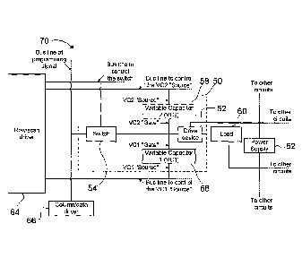
Figure 1 illustrates a threshold electrical stability compensation apparatus
or circuit
50, in accordance with an embodiment. In this embodiment, the electrical
stability
compensation apparatus 50 is shown in an array 70 in which common programming
signals
and a common power supply may be used among a plurality of electrical
stability
compensation apparatuses 50. The array 70 may represent a pixel array in a
light-emitting
display and the electrical stability compensation apparatus 50 may represent a
pixel element.
It will be understood that the electrical stability compensation apparatus 50
may also be
generalized to other applications where compensation for electrical
instability may be useful.
For example, the electrical stability compensation apparatus may be used with
inorganic LEDs of a wide band gap semiconductor material for ultraviolet (UV)
light
disinfectants for water purification. In the UV water purification example,
the apparatus is
intended to provide an optimal brightness for efficient antibacterial water
sanitation.
In a further example, the electrical stability compensation apparatus may be
used in a
piezoelectric device such as a membrane actuator for providing vibrational
motion. In the
piezoelectric device, the apparatus is intended to provide consistent
amplitude generation of
acoustic wave propagating devices such as micro-electro-mechanical systems
(MEMS).
In Figure 1, the array 70 includes a load 60 (e.g., a light-emitting device,
such as an
OLED). The apparatus 50 includes a drive device 52 (e.g., a transistor, such
as a TFT) to
control a drive signal (e.g., drive current) from a power supply 62. The drive
device 52
controls a characteristic (e.g., luminance) generated by the load 60. The
apparatus 50 also
includes a switch 54, a first variable capacitor 56 (VC1), and an optional
second variable
capacitor 58 (VC2). A gate of the first variable capacitor 56 is connected to
a gate of the
drive device 52. A gate of the second variable capacitor 58 is connected to
the gate of the
8
CA 02827959 2013-09-20
drive device 52. It will be understood that, for a color display, each pixel
may comprise a few
sub-pixels generating different colors.
The variable capacitor 56, 58 is a component with at least two terminals,
including a
gate and a source (as defined herein) of the variable capacitor 56, 58. The
variable capacitor
56, 58 has a threshold voltage (VT) and a gate-to-source voltage (Vgs). The
Vg, of the variable
capacitor 56, 58 is a voltage difference between the gate and source of the
variable capacitor
56, 58. Which terminal is the gate of the variable capacitor 56, 58 and which
terminal is the
source of the variable capacitor 56, 58 is defined such that the definition of
the Vg, of the
variable capacitor 56, 58 is in accordance to the following descriptions of
the dependence of
the capacitance of the variable capacitor 56, 58 on the Vg, of the variable
capacitor 56, 58.
The capacitance of the variable capacitor 56, 58 may be dependent on the Vgs
of the variable
capacitor 56, 58. For example, the capacitance of the variable capacitor 56,
58 when Vgs is in
a range whose lower boundary is higher than or equal to VT may be larger than
the one when
Vg, is in a range whose upper boundary is lower than or equal to VT. When
Vgs>VT, the
variable capacitor 56, 58 may be indicated as ON. When Vgs<VT, a variable
capacitor 56, 58
may be indicated as OFF. A charge stored in the variable capacitor 56, 58 may
vary with the
change of the characteristics (e.g. capacitance, VT, etc.) of the variable
capacitor 56, 58.
The array 70 includes row scan driver 64 and column data driver 66, which
control the
switch 54, and variable capacitors 56, 58. The electrical stability
compensation apparatuses
50 in the same row may be controlled by the same row driver 64, and the
electrical stability
compensation apparatuses 50 in the same column may be controlled by the same
column
driver 66. There are a few ways to drive the array 70. For example, electrical
stability
compensation apparatuses 50 may be programmed row-by-row: first, the
electrical stability
compensation apparatuses 50 in a row are configured into a programing phase by
the
corresponding row driver 64; then, they are programmed respectively by the
signals provided
by the corresponding column drivers 66. After the programming of one row of
electrical
stability compensation apparatuses 50 is completed, the corresponding row
driver 64
configures the electrical stability compensation apparatuses 50 in the row
into a driving phase
to let the electrical stability compensation apparatuses 50 generate their
respective drive
signals (e.g., drive currents) to control the loads 60 to generate their
respective characteristics
9
CA 02827959 2013-09-20
(e.g., luminance) as programmed in the programming phase. In the meantime, the
electrical
stability compensation apparatuses 50 in the next row are configured into the
programming
phase by the row driver 64 of the next row, and same cycle repeats.
In the array 70, bus lines of the switch 54 and the first and second variable
capacitors
56, 58, respectively, can be shared by electrical stability compensation
apparatuses 50 in the
same row and connected to the row driver(s) 64. Bus lines of the programming
signals can be
shared by the electrical stability compensation apparatuses 50 in the same
columns and
connected to the column driver(s) 66. The power supply 62 and ground
connections may be
shared by all electrical stability compensation apparatuses 50 in the array
70.
Figure 2 illustrates a threshold electrical stability compensation apparatus
or circuit
100, in accordance with an embodiment. In this example, the circuit 100 is a
pixel circuit for
use with a display. The pixel circuit 100 includes a drive transistor 102
(To), a switch
transistor 104 (Ti), a first variable capacitor 106 (T2), a second, optional,
variable capacitor
108 (T3), and a load 110 such as a light emitter, for example, an OLED. The
transistors 102,
104 may be implemented by using different types of transistors, for example, n-
type or p-type
thin-film transistors (TFTs).
One of, or both of the variable capacitors 106, 108 may be TFT-based metal-
insulator-
semiconductor (MIS) capacitors constructed by connecting a source and a drain
of n-type or
p-type TFTs, respectively. An n-type TFT with its source and drain being
connected together
is an example of a variable capacitor. In this case, the gate terminal of the
variable capacitor
106, 108 can be defined as the gate of the TFT; the source terminal of the
variable capacitor
106, 108 can be defined as the source of the TFT, which is connected to the
drain of the TFT.
As a particular example, when the gate-to-source voltage of the n-type TFT is
higher
enough than its threshold voltage, the total capacitance of the n-type TFT is
equal to the
channel capacitance plus the sum of the source and drain overlap capacitances.
When the
gate-to-source voltage of the n-type TFT is lower enough than its threshold
voltage, the total
capacitance of the n-type TFT is equal to the sum of its source and drain
overlap capacitances.
When the gate-to-source voltage of the n-type TFT is higher than its threshold
voltage, the
amount of the charge stored in the n-type TFT decreases with the increase of
its VT.
CA 02827959 2013-09-20
The drive transistor 102 is configured to control the load current 111 in a
driving
phase (I:17) from a power supply 112 (VDD) to the load 110. The switch
transistor 104 is
configured to control the access from an external programming voltage driver
114 (Vprog),
which may be included in a column data driver (e.g., the column data driver 66
of Figure 1),
to a node A 116 in the pixel circuit 100. The external programming voltage
driver 114
provides a programming signal to the node A 116 via the switch transistor 104.
In the programming phase, the first variable capacitor 106 releases a charge,
and the
second variable capacitor 108 stores a charge. In the driving phase, the first
variable capacitor
106 is configured to generate the compensation voltage to compensate for the
AVT of the
drive transistor 102 so as to stabilize the drain-to-source current 111. The
first variable
capacitor 106 provides compensation for the AVT of the drive transistor 102 by
drawing
charge from node A 116. The second variable capacitor 108 is configured to
inject charge
onto node A 116 and the gate of the drive transistor 102 to improve the load
current (or drain-
to-source current of the drive transistor) 111.
The gate voltage stress applied on the drive transistor 102 results in the AVT
of the
drive transistor 102. If the AVT of the drive transistor 102 is not
compensated, it causes the
change of the drain-to-source current 111.
Since the gate of the first variable capacitor 106 and the gate of drive
transistor 102
are stressed by the same voltage (i.e., the voltage on node A 116), the AVT of
the first variable
capacitor 106 tracks the AVT of the drive transistor 102. The AVT of the first
variable
capacitor 106 results in the change of the charge drawn by the first variable
capacitor 106
from the gate of the drive transistor 102 in the driving phase, and therefore
results in the
change of the gate voltage of the drive transistor 102 with the AVT of the
drive transistor 102.
Since the AVT of the first variable capacitor 106 tracks the AVT of the drive
transistor 102, in
the driving phase, the change of the gate voltage of the drive transistor 102
compensates the
AVT of the drive transistor 102. AVT of the drive transistor 102 is
compensated such that the
drain-to-source current 111 does not change with the AVT of the drive
transistor 102. The
stability of the drain-to-source current 111 in the driving phase is improved
by using the first
11
CA 02827959 2013-09-20
variable capacitor 106 to generate the compensation voltage so as to
compensate for threshold
voltage shift of drive transistor 102.
Optionally, the second variable capacitor 108 may be provided to inject charge
onto
the gate of the drive transistor 102 to improve the drain-to-source current
111. The second
variable capacitor 108 may be needed to improve the drain-to-source current
111 to the levels
that may be desirable in some practical designs.
Where the second variable capacitor 108 is not provided, the pixel circuit 100
can
generally compensate the AVT of the drive transistor 102. However, in this
case, the drain-to-
source current 111 may be relatively lower, which may be a drawback if higher
current levels
are desired. On the other hand, because the footprint needed for the second
variable capacitor
108 is saved, it may be possible to enlarge the area of the light-emitting
device and the
aperture ratio of display can be improved, which may be an advantage if higher
aperture ratio
is desired.
Figures 3 and 4 illustrate a driving scheme 200 and a method 201,
respectively, for
electrical stability compensation in accordance with an embodiment herein. The
driving
scheme 200 and method 201 illustrated each include one frame cycle and each
frame cycle
may include a programming phase 202 and a driving phase 204. The driving phase
204 is
typically much longer in duration than the programming phase 202. It will be
understood that
the driving scheme 200 and method 201 may also have other phases, for example,
an idle
phase and/or an intermediate phase.
When the programming phase 202 begins, the switch transistor 104 is turned on,
at
206, by a voltage VIII, connecting node A 116 to the programming voltage
driver 114. The
first variable capacitor 106 is turned OFF, at 208, by a voltage V2H such that
a charge is
released from the first variable capacitor 106. The second variable capacitor
108 is turned
ON, at 210, by a voltage V3L and thus stores a charge on its gate.
A gate charge of a transistor may be divided into a gate charge due to the
gate-to-
channel capacitance (Qch) and a total gate charge due to the overlap
capacitance between gate
and source/drain (Q.,). After voltages and/or currents reach the program set-
points, at 212,
the drive transistor 102 is in the saturation mode, the first variable
capacitor 106 is OFF, the
switch transistor 104 is in the triode mode, and the second variable capacitor
108 is ON. The
12
CA 02827959 2013-09-20
gate-to-channel capacitance of the drive transistor 102 can be expressed as
Equation 1 where
Ci is the channel capacitance per unit area, Wo, Lo, and VT,0 are the width,
length, and
threshold voltage of the drive transistor 102, is
is the set-point load voltage (for example,
OLED voltage), and Vdata is the data voltage provided by Vprog. For the same
expected
Vdata is provided with the same corresponding value, not changing with V1,0.
The coefficient
2/3 is used in Equation 1, as a typical assumed theoretical value, because the
drive transistor
102 is biased in saturation mode. The actual value of the coefficient may
depend on the
specific process technology and properties of the transistor.
QP"g 2/3C-W
ioLO (Vaa
dt ¨ V/9)27 D VT,0)
ch,0 Eq. 1
In the programming phase 202, the first variable capacitor 106 is OFF, so its
(XII is
zero. V11', V21, V3L Vdata, and VDD do not change with AVT,o. AVT,i and AV1,3
are negligible
when compared to AVT,o (see Equation 19 and 20 below). The AV caused caused
by VT,0 is
negligible (see Equation 17 below). Therefore, in the programming phase 202,
the Qch of the
switch transistor 104 and the second variable capacitor 108 (i.e., Q 7h7ig and
Q 7h7) as well as
the Q0, of all TFTs 102, 104, 106, 108 do not change with AVT,o, so they are
not included in
the analysis of the changes of the charge components with AVT,o=
In the driving phase 204, the switch transistor 104 is turned off, at 214, by
voltage V11'
,
isolating the node A 116 from the programming voltage driver 114. The first
variable
capacitor 106 is turned ON, at 216, by voltage V2L, providing AV1,0-
compensation. The
second variable capacitor 108 is turned OFF, at 218, by voltage V3H, injecting
a charge to
node A 116 to boost the gate voltage of the drive transistor 102 so as to
improve the load
drive current 111. To conserve the charge on node A 116, the switch transistor
104 is turned
OFF before switching V2 and V3.
While the switch transistor 104 is being turned off, a part of the switch
transistor's
channel electrons are injected to node A 116: Q 71,1ZA ¨13Q C7.p is close to
1/2 if V1 has a
high falling rate. Since Q fi does not change with AVT,o, QT7 is not included
in the
13
CA 02827959 2013-09-20
analysis of the changes of the charge components with AV1,0. After node
voltages settle
down, at 220, the drive transistor 102 is in the saturation mode, the first
variable capacitor 106
is ON, and the switch transistor 104 and the second variable capacitor 108 are
OFF. The Qeh
values of the drive transistor 102 and the first variable capacitor 106 can be
expressed as by
Equations 2 and 3 where V /To" is the set-point voltage on node A 116, and
Voctill is the set-
point voltage across the load 110 (for example, an OLED). Since the switch
transistor 104 and
the second variable capacitor 108 are OFF, their Qch values are zero.
Q driv 2 13CittroLo (Virjjv Vc(IrAD ¨ VT ,0)
cd:13 = eiT472L2 ¨ ¨ T .2)
Eq. 2, 3
The Q0, values of the transistors 102, 104, 106, 108 are given by Equations 4
to 7
where Co, is the unit-area source/drain overlap capacitance, L0 is the overlap
length between
the gate and source/drain, and QdriL is the gate charge of the switch
transistor 104 due to
the overlap capacitance on the side of node A 116.
Qdr tql/driv 17driv
ooi,ov
CovIVoLouv.,vG,0 voLED ¨ 1,TDD),
Q (vdri TiL\
v (v A,1
dyriv =__
1471 Lot, k v Gs) ¨ )1
Q
driv v L
odtr,i1 2C ov147 V
2¨ov \G,0 ¨ v2 I,
Q od rvi 3v = ry
W3Lov (Vgroiv 17,311) Eq. 4,
5, 6, 7
Where the pixel circuit 100 is switched from the programming phase 202 to the
driving phase 204, Equation 8 can be derived based on the charge conservation
on node A
116. c or. i of can be expressed as Equation 9. Although other charge
components may also
contribute to the charge conservation on node A 116, they may not vary with
AVT,oand thus
are not included in Equation 8.
d(2511 ______________________________ dC2deTit2 cl(2`011r,i1+0t
cli/T 0 d
= dV V
T,0 dVT,0 T.0
Eq. 8
ndr iv ndrivndriv ndriv _j_ rynvtri
ov ,T ot tcC ,0 A ov ,2 1
-4c Eq. 9
14
CA 02827959 2013-09-20
The current IDs of the drive transistor 102 when it operates in saturation
mode can be
expressed by Equation 10 where aSAT, p, 'Y, and VAA are device parameters.
W (VGS VT)7+2
a S AT itinLit
AA Eq. 10
Therefore, when VT,0 shifts, the condition required to stabilize /04/41 can be
expressed
as Equation 11.
,Tudriv ,
GS,0 1 (-6 v T,0 ¨ Eq. 11
Since Vs,o = VOLED and dV LErividvT,0 = 0 (see Equation 18, below), Equation
11 is
equivalent to Equation 12.
dudriv / v õ
u' G,0 m-
T,0 = 1 Eq. 12
When AVT,o is fully compensated by ZtVdas,70' = AVT,o, the channel charge of
the drive
transistor 102 in the driving phase 204 does not change with AVT,o which is
described by
Equation 13.
dQJ/dVT,0 =0 Eq. 13
Substituting Equation 13 into Equation 8 yields Equation 14.
A2cPiriog dQdriv dndriv
eh 2 ov,T ot
dVT,0 dV1,0 Eq. 14
Substituting Equations 1-7, and 9 into Equation 14 and then using the relevant
formulas presented below yields Equation 15, which gives the parameters that
specify the
width of the first variable capacitor 106, where Cov,n= CovWnLov (n = 0, 1, 2,
3).
2/ 3Ci WoLo 2Cov,o Coto + 2Cov
14/2 = /2CiL2 ¨ 2Cov-Lov Eq. 15
The AVT,0- compensation can be achieved by sizing the first variable capacitor
106 as
specified in Equation 15. For the variable capacitors 106, 108 fabricated by
using different
process technologies or facilities, and/or designed to have different
properties (for example,
CA 02827959 2013-09-20
=
different geometries, structures, shapes, features, etc.), the coefficient
values (e.g. 2/3) may be
adjusted according to the procedure as outlined above. The coefficient values
(e.g., 2/3, 1/2,
2, etc.) used in the above procedures may be process/technology-dependent
and/or design-
dependent. Although the coefficient value may be adjusted in a specific
design, the
procedures as outlined above may still be valid for circuit analysis and
design.
VT,0-compensation mechanism is explained by analyzing Equation 8, where VT,0
shifts but the change in VT,0 is compensated. ecr:: reduces when VT,0
increases (i.e., the
increase of VT,0 results in less channel charge stored in the drive transistor
102 in the
programming phase 202).
dru
To compensate for AVT,o, AV G,0 should be as large as AVT,o. Since Q :a,:
increases
with V d;:oiv, more charge may be needed to be provided to the gate-to-
source/drain overlap
capacitors which belong to transistors 102, 104, 106, 108 and connect to the
node A,
otherwise V dGr.olv may not be able to increase with VT,0. Since VT,2
increases faster than V Is";
Qdill' decreases when VT,0 increases.
ch,2
Designing W2 as specified in Equation 15 validates Equation 14. This means
that,
when VT,0 increases, the decrease of Q 2 is so large that it not only cancels
out the decrease
4riv
of Q yig but also provides the extra charge needed by the increase of Q As
a result, Q
does not change with VT,0, SO /337dosrlov is as large as AV1,0. Since AVT,0 is
fully compensated by
driV it does not affect I dra7
GS ,05 GLED=
To demonstrate the effectiveness of the pixel circuit 100, circuit simulations
were
carried out on the pixel circuit 100, which was driven by the drive scheme 200
and method
201. Simulations were carried out using a Cadence Spectre circuit simulator
and a-Si:H TFT
model where eff 0 .3CM2 N s, V inrit = 3V, Ci = 19nF/cm2, and C, = 16nF/cm2,
and the OLED
model fitted to the measured data of OLED I¨V characteristics. dr is the
transistor effective
mobility, and V IV is the VT for a fresh transistor before being electrically
stressed.
16
CA 02827959 2013-09-20
=
Parameter Value Parameter Value
Programming Phase (as) 120 Vdata (V) 10 ¨ 25
147o/Lo (pm) 100/25 VDD (V) 30
Wi/Li (pm) 50/25 Vi (V) 0 30
1412/L2 (Iim) 60/100 V2 (V) 2 ¨ 30
1/1/3/L3 (pm) 35/100 V3 (V) 2 , 30
Lot, (pm) 5 41)1ZID (pA) 0 ¨ 3
TABLE I
The parameter values of the simulated pixel circuit 100 are listed in Table I.
The
parameter values listed are exemplary values used in the simulation. It will
be understood
that other parameter values may be used. The minimum channel length was
selected as
25gm. Values as small as 0.5 gm to 1 mm may be used as minimum channel length.
The
minimum channel length of the transistors 102, 104, 106, 108 may be selected
as needed in a
specific design. Based on the simulation results, W2 := 60gm was determined as
a preferred
value for AVT,o-compensation in the simulated example of the pixel circuit
100. Values for
W2 may range from 0.5 gm to 1 mm. Transistors 102, 104 and/or variable
capacitors 106,
108 may be scaled up or down to any desirable level, and the scaling may not
affect AVT,o-
compensation. Where the transistors 102, 104 and/or the variable capacitors
106, 108 are
scaled down, their footprint may be reduced, such that the performance of the
pixel/display
may be improved, for example improved response speed, refresh rate,
resolution, power
consumption, display panel size, aperture ratio etc.
To verify the AVT,o-compensation, AVT,0 was varied in simulations, and AV1,2
was set
as AV1,2 = 3/2AV1,0. The degradations of the switch transistor 104, the second
variable
capacitor 108 and load 110 were neglected.
Figures 5 and 6 are graphs 500, 600, respectively, of simulation results of
the pixel
circuit 100 showing charge components 502, 602 versus AVT,0504, 604 (in
Equation 8) for
Vdata= 25V and 10V, respectively. When AVT,0 504 increases, AQ dc,Z; is so
large that it equals
AQ, AQ :;:so Qdcrh! (IL does not change with AVT,o504. Figure 6
illustrates, for Vdata =
17
CA 02827959 2013-09-20
10V, that AVT,0 604 is not always fully compensated. For AVT,0> 2.25V, Q
dcri:ov starts to drop,
indicating LW dGrs.'01; < AVT,o. This is referred to as the under-compensation
of AVT,o 604.
Figure 7 is a graph 700 showing LW 4G7s!c;* 702 versus Vdata 704 for different
AVT,0 706 of
the simulated pixel circuit 100. Figure 8 is a graph 800 of simulation results
of the pixel
circuit 100 showing IodLEril 802 versus Vdata 804 for different AVT 806.
Figure 7 illustrates that
for relatively high Vdata 704, LW dasr!av = AVT,0 706, so AVT,0 806 does not
affect I od t , as
illustrated in Figure 8.
Figure 9 is a graph 900 of simulation results of a conventional voltage
programmed 2-
transistor pixel circuit showing IodLrE'r 902 versus Vdata 904 for different
AVT 906. Figure 9
illustrates that since there was no AVT,o-compensation, I odult; 902 dropped
significantly with
the increase of AVT,0 906. The comparison between Figure 8 and Figure 9 shows
the
effectiveness of the pixel circuit 100 in AVT,0-compensation as compared to a
simulated
conventional voltage-programmed 2-transistor pixel circuit.
Figure 10 is a graph 1000 of simulation results of the detail of Figure 8
showing I oci 11
1002 versus Vdata 1004 for different AVT 1006. For lower Vdata 1004 and Iod ur
D' 1002, the
under-compensation of AVT,0 1006 appears at lower AVT,0 1006, as shown in
Figures 6, 7, 8,
and 10. This can be explained based on Equation 22, which indicates that VT,2
increases with
VT,(9. For a smaller Vdata, V acsril is also smaller, so the AVT,0 at which
VT,2 increases up to
Vdosr ,11; is smaller. Once VT,2 catches up with V dcZ, Q der; becomes zero
and thus stops
dr-it
decreasing with the increase of AVT,0, so Q cla starts to drop with the
increase of AVT,0 (see,
e.g., Figure 6). This indicates that V d;57 < AV T ,0 (i.e., AVT,0 is under-
compensated (see, e.g.,
Figure 7)). So 1od a starts to drop with the increase of AV1,0 (see, e.g.,
Figure 10). If AVT,0
18
CA 02827959 2013-09-20
is not too large, the under-compensation of AVT,0 exists only at the lowest
ill levels (see,
e.g. Figures 7 and 8), so it does not affect the overall stability of!
While dVT,2/dVT,0 3/2 was assumed, this approximation may have a discrepancy
up
to 10%. Discrepancy factor (Fd,$) is the factor defined to describe the
discrepancy of the
actual value of dVT,2/dVT,c, away from 3/2, which is the assumed theoretical
value of
dVT,2/dVT,O. Fdis is defined so that dVT,2/dVT,0 = (3/2)Fd1õ where Fdis is
within a range from
0.9 to 1.1. Correspondingly, Equation 15 becomes Equation 16.
2C0 +C,, 1 + 2G,3
11'2 =
(3/2Fdt, ¨ 1)C,L2 ¨ 2CorLor Eq. 16
Figure 11 is a graph 1100 of simulation results of the pixel circuit 100
showing
normalized simulation results of Ioda"'D 1102 versus AVT,o 1104 for \Idea =
25V. Figure 11
illustrates the impact of the variation in Fdis 1106 on the stability of 7 od
LEr I 1102 for a W2 value
driv
designed by assuming Fdis = 1. For Fdis > 1, AVT,0 1104 is over-compensated,
so I cnsz 1102
increases with AVT,0 1104. For Fdis < 1, the opposite trend exists. For Fdis e
(0.9, 1.1), the
instability of 70%1 1102 is within 8%. In design practice, the value of Fdis
1106 may be
extracted from measurement results and then used in Equation 16 to achieve a
more accurate
1\VT,0-compensation.
If the second variable capacitor 108 is not used, since the first variable
capacitor 106
draws charge from node A 116 after the driving phase 204 begins, V'Z'a,*vmay
be lower than
dev
what is needed by the ollevels desired in practical designs. Therefore, the
second variable
capacitor 108 may be used to improve I õtit; levels. In the programming phase
202, the
second variable capacitor 108 is turned ON at 210 by V31 and stores charge on
its gate. In the
driving phase 204, V3 is switched to V3H, at 218, to inject the charge from
the gate of the
second variable capacitor 108 onto node A 116, improving 1/ tr: and therefore
/ LEI. The
improvement I otrz, can be adjusted by varying the size of the second variable
capacitor 108.
Q 71,7 is the gate charge associated to the channel of the second variable
capacitor 108.
It is stored on the gate of the second variable capacitor 108 in the
programming phase 202 and
19
CA 02827959 2013-09-20
injected onto node A 116 in the driving phase 204. Since V3L is a fixed value
shared by all
pixels in the same row, Q .71 is determined by the specific Yam for the pixel.
QP,71 does not
change with AVT,o, so it does not affect AVT,o-compensation. The impact of the
usage of the
second variable capacitor 108 on AVT,o-compensation is due to C0,3. However,
this impact is
minor because C0v,3 is a parasitic component. Assuming Cov = C1, using the
geometries in
Table I, one can see that C0v,3 is 3.55% of the total capacitance on node A
116 in the driving
phase 204.
Figure 12 is a graph 1200 of simulation results of the pixel circuit 100
showing Igal
1202 versus Vdata 1204 for different W3. Figure 12 illustrates simulation
results which
confirm that increasing the size of the second variable capacitor 108 improves
I 1202
without significantly affecting AVT,o-compensation.
Figure 13 is a graph 1300 illustrating simulation results of the pixel circuit
100
showing VG,0(t) 1302 versus time 1304, for AVT,0 =OV and different initial
values of VG,0(t) in
a programming phase 202. Figure 13 illustrates the simulation results of
VG,0(t) in the
programming phase 202 to demonstrate the programming speed of the pixel
circuit 100. The
waveforms of VG,0(t) are dependent on the initial value of VG,0(t) in the
programming phase
202, which is in turn the value of VG,0(t) after it reaching the set-point in
the last driving phase
204 (denoted as V drtn. According to the simulation results shown in Figure
15, for AVT,o
= OV, VT: ranges from 6V to 18V, so the waveforms of VG,0(t) were simulated
for 17 drtoEcsr =
6V and 18V, respectively. Figure 13 shows that VG,o(t) settled down within 99%
of Vdata in
90 s. For the other corner AVT,0 = 5V, simulations verified the same
conclusion. If the sizes
of the devices (e.g., transistors, variable capacitors, or light-emitting
device) are scaled down,
the programming speed may increase.
Assuming the drive transistor 102 and load 110 (for example, OLED) have the
typical
sizes and the same stress conditions, referring to their degradation models
and data, one can
see that AVOLED is much smaller than AVT,o. Due to the steep OLED I ¨ V
characteristic, the
AV PcTLE 11, caused by AVT,0 is negligible as shown in Equation 17.
0.
Eq. 17
CA 02827959 2013-09-20
Figure 14 is a graph 1400 of simulation results of the pixel circuit 100
showing the
17Pr 9
following curves for G,0 = 16.7V: (1) the curve of load current 1402 versus
load voltage
1404 in the programming phase; and (2) the two curves of the drain-to-source
current 1402 of
the drive transistor (i.e., IDs,o) versus the source voltage 1404 of the drive
transistor (i.e.,Vs,o)
in the programming phase for AVT,0 = OV and AVT,0 = 5V, respectively. V
0PLE"re (i gisr, and
V Pf" (1Pmg r) are the load voltages (currents) in the programming phase 202
for AVT,0 = OV
OLEO OLED
and 5V, respectively, and AVPLccgz = (V ¨
V MP' For AVT,0 = 5V, Figure 14 shows that
AV Pr 91 = 0.292V, which is only 5.84% of AVT,o, so Equation 17 is reasonable.
OLED
In the driving phase 204, assuming AVT,0 is already fully compensated, for the
same
Vdata, :It does not change with AVT,o, so V odLrEi/ does not change with VT,O
as shown in
Equation 18.
dVMD /di/To = O.
Eq. 18
For a practical display with N rows of pixels, the total stress time spent in
the
programming phases 202 is only 1/N of that spent in the driving phases 204.
For a practical
refresh rate (for example 60Hz) the effects of negative pulse gate-to-channel
stress voltages
on AVT are much smaller than those of positive pulse gate stress voltages.
This implies that
only the AVT of the transistors 102, 104 and variable capacitors 106, 108
stressed by positive
gate-to-channel voltages in the driving phase 204 need to be considered.
Therefore, AVT,i and
AVT,3 can be considered as negligible when compared to AVT,0 and AVT,2 as
shown in
Equations 19 and 20.
0.
dt'T.,/,tvr,0
Eq. 19,20
Since the gates of the drive transistor 102 and the first variable capacitor
106 are
connected, their gate voltages are the same. Their source voltages in the
driving phase 204 can
be made approximately the same. V21- is a fixed value provided by the row
driver. V guril is
not fixed because it depends on Vdata. However, due to the steep OLED I ¨ V
curve, the
21
CA 02827959 2013-09-20
variation range of V a' is much narrower than that of V dGroic. V2L is
selected as a value close
to vsince v dcsrv (v _ odrcvd and v drt; = (v dzroicr V ,21,µ
) Equation 21 can be derived.
OLRE'
Va% VS; -
Eq. 21
Figure 15 is a graph 1500 of simulation results of the pixel circuit 100
showing Vd;olv
and VOLED driv 1502 versus Vdata 1504. Figure 15 justifies Equation 21 by
simulated results. V 21'
is selected as 2V to make it lower than but still close to the range of V od .
This is to provide
that V dGsn; > V 4;:si; to make VT,2 shift faster than V1,0 in the pixel
circuit 100.
Figure 16 is a graph 1600 of simulation results of the pixel circuit 100
showing
driviv driv
1602 versus Vdata 1604. Figure 16 shows that V 'L71'17 V drtv 1602 is around
or
C-1,2 CS,0 CS,2
lower than 1.1, so Equation 21 is justified.
AVT,0 and AVT,2 depend on the respective electrical stress history of the
drive
transistor 102 and the first variable capacitor 106. The transistor
degradations caused by
and VTT: can be neglected because of the short duration of the programming
phase 202. In
the driving phase 204, the drive transistor 102 is stressed in saturation
mode, but the first
variable capacitor 106 which is implemented, for example, as a TFT with the
source and drain
connected together, is stressed in triode mode. Since ilts"',=--'007;,1
Equation 22 is given.
dvi,advr, 2/3.
Eq. 22
Substituting Equation 21 and 22 into Equation 11 yields Equation 23.
2/3.
Eq. 23
Figure 17 illustrates an optical micrograph 1700 of a fabricated pixel circuit
having the
design of the pixel circuit 100, to verify AVT,0-compensation. In stress
tests, VDD = 20V and
Vdata = 15V were used. The low and high levels of the voltage signals VI, V2,
V3 were zero
and 20V, respectively. Since the primary test purpose was to verify AVT,o-
compensation, the
OLED mimic (i.e., the diode-connected transistor) was excluded by setting Vss
as open-
22
CA 02827959 2013-09-20
drtv
circuit. 105,0 was measured from pad Vs,o, whose level was kept at virtual
ground. The
driv
measured I Du before the stress test was 1.05pA.
Figure 18 is a graph 1800 of measurement results showing normalized IDdrs.t;
1802
versus stress time 1804 for the pixel circuit 100. For comparison, a stress
test was carried out
on another sample of the same pixel circuit design whose AVT,0-compensation
was disabled
by fixing V2 and V3 at 20V. Therefore, the sample acted like a conventional
voltage
programmed 2-transistor pixel circuit. To make the circuit also have the
initial I :";-=
1.05[tA, its Vdata was set to 15.5V. The environment temperature of the stress
tests was 40 C.
Figure 18 illustrates that the overall stability of the I V; with AVT,0-
compensation 1806 is
improved over the one of the circuit without AVT,o-compensation 1808. Note
that even with
AVT,0-compensation 1806, I 4,37; still has some residual instability. It could
be caused by some
second-order effects, including non-zero AVT,i and AVT,3, and/or minor
variations of
(AVT,2/AVT,o) throughout the test.
Figure 19 is a graph 1900 of measurement results of the capacitance 1902
versus
voltage 1904 (C-V) characteristics of the transistors 102, 104, and the
variable capacitors 106,
108 stressed with AVT,0-compensation, before and after the 240-hour stress
test. The upper
graph 1906 is for the C-V curves of the drive transistor 102 and the first
variable capacitor
106. The lower graph 1908 is for the C-V curves of the switch transistor 104
and the second
variable capacitor 108. The assumptions about the AVT of transistors used in
analysis were
verified by the measurement results. As shown in Figure 19, after a 240h-
stress test, AVT,o
2.15V and AVT,0 3.15V, which illustrates that the ratio is close to the
assumed 2/3. As
AVT,1 and AVT,3 are much smaller than AVT,0 and AVT,2, it may be acceptable to
neglect AVT,i
and AVT,3 in a first-order analysis.
Figure 20 is a graph 2000 showing a measured transfer curves of the drive
transistor
102 (i.e., IDS, 02002 versus Vcs, 02004) in the circuit 100 stressed with
AVT,0-compensation,
before and after the 240-hour stress test. The extracted VT,0 2V is close to
the result from
capacitance versus voltage (C-V) measurement. AVT,oresults in significant
Ips,0 drops if
AVT,o-compensation is not used.
23
CA 02827959 2013-09-20
Figure 21 is a graph 2100 showing a measured IDdrs; 2102 versus Vdata 2104 of
the
pixel circuit 100 stressed with VT,0-compensation, before and after the 240-
hour stress test.
Figure 21 shows that, when AVT7compensation is used, except for the lowest
ID420' levels, the
Id4ov differences caused by AVT,0 are insignificant. There is under-
compensation on the lowest
ILI levels (zero to 0.15gA).
Figure 22 is a graph 2200 of measurement results of V1 2202, V22204, V32206,
Vprog
2208 (switching from high level to low level (i.e., and low level to high
level (i.e.,
L--4I), respectively), and transient behavior of Ids,0 2210 in the pixel
circuit 100 before and
after applying a 240-hour stress test. As shown in Figure 22, the programming
speeds of the
pixel sample with AVT,0-compensation were measured before 2212 and after 2214
the 240h-
stress test, for Vprog going from 5V to 15V (Vprog L ---> H) and from 15V to
5V (Vprog : H -->
L). In all cases, Ips,0 2210 in the programming phase 202 settled down within
95% of the
final value in 25011s.
The AVT of the drive transistor 102 due to electrical stress is compensated by
the
change of gate-to-source voltage (AVgs) of the drive transistor 102 generated
by the AVT-
dependent charge transfer from the drive transistor 102 to the first variable
capacitor 106. The
charge injection from the second variable capacitor 108 to the gate of the
drive transistor 102
in driving phase 204 improves the load drive currents 111. Advantages include
that only one
transistor is in series with the load 110, reducing static power consumption.
The driving
scheme 200 allows fast programming speed, simple control signals, and simple
external
driver. Since the pixel itself compensates the AVT of the drive transistor
102, there is no need
for the compensation from an external driver, reducing the design complexity.
There may
also be no need for optical feedback, avoiding problems with photo-sensor
instability and
light interference. As each pixel has its own AVT-compensation, higher
resolution
compensation may be achieved.
The structure of the pixel circuit 100 could be less complex compared to other
compensation circuits and utilizes current manufacturing techniques. The
driving scheme 200
of the pixel circuit 100 is also generally simplified compared to similar
circuits intended for
similar purposes.
24
CA 02827959 2013-09-20
The pixel circuit 100 is intended to compensate for electrical instability of
the drive
transistor 102 with fast programming speed, simple control signals, simple
circuit structure,
and low static power consumption, which are desirable for commercialization of
various
systems, such as AMOLED technology. The pixel circuit 100 may provide more
uniform
display brightness over large screens (e.g., AMOLED Television) and longer
operational
lifetimes for displays while using lower power consumption and potentially
lower cost driver
electronics. The pixel circuit 100 may be used in devices such as televisions,
computer
monitors, mobile-phone displays, near-eye displays, cameras, personal media
players, medical
displays, flexible displays, transparent displays, etc.
The pixel circuit 100 may reduce the cost of AMOLED display products while
also
increasing the pixel lifetime of AMOLED displays by providing compensation
with faster
programming speed. It may also be possible to use mature low-cost fabrication
technology
(e.g. amorphous silicon TFT) to produce large-size AMOLED display panels using
this
technology. The cost impact is intended to be negligible as integration of the
pixel circuit 100
may not affect manufacturing or assembly costs.
The circuit 50 or 100 may be useful for any circuit in which a change of the
gate
voltage of a transistor is needed to compensate for
instability/degradation/variation of the
transistor.
Figure 23 illustrates a circuit 2300, in accordance with a further embodiment.
The
circuit 2300 differs from the circuit 100 of Figure 2 in that a load 2310
(e.g. an OLED) is
placed between a power supply (VDD) 2312 and the drive transistor (To) 2302.
The driving
scheme of the circuit 2300 is as described with reference to Figures 3 and 4.
With the circuit
2300, the OLED instability does not affect the operation of the drive
transistor 2302 so the
stability of a load driving current 2311 may be improved.
Figures 24 and 25 illustrate a circuit 2400 and a driving scheme 2500, in
accordance
with another embodiment. The circuit 2400 has a switch transistor (Ii) 2404
and a first
variable capacitor (T2) 2406 sharing a common control signal V1,2. The circuit
2400 saves
one bus line in the row direction, so the aperture ratio of a display panel
may be improved and
the design of row/scan driver may be further simplified.
CA 02827959 2013-09-20
Figures 26 and 27 illustrate a circuit 2600 and a driving scheme 2700, in
accordance
with yet another embodiment. The circuit 2600 has a drive transistor (To) 2602
and a second
variable capacitor (T3) 2608 sharing a common control signal VDD 2611. The
circuit 2600
saves one bus line for each row of pixels, so the aperture ratio of a display
panel may be
improved.
Figures 28 and 29 illustrate an array 2800 and a driving scheme 2900, in
accordance
with another embodiment. The array 2800 has every two neighboring rows of
pixels 2818,
2820 sharing V2 2822 and V3 2824. The circuit 2800 saves two bus lines for
every two rows
of pixels 2818, 2820, so the aperture ratio of a display panel may be
improved.
Figure 30 illustrates a circuit 3000, in accordance with another embodiment.
The
circuit 3000 includes a first capacitor 3026 (C2) and a second capacitor 3028
(C3) which are
respectively regulated by third and fourth transistors 3006, 3008. The first
and second
capacitors 3026, 3028 may be non-variable capacitors, metal-insulator-metal
capacitors, MIS
capacitors, or other types of capacitors. The driving scheme of the circuit
3000 is as
described with reference to Figures 3 and 4.
The first variable capacitor 56 in the electrical stability compensation
apparatus 50
may be implemented as a combination of the first capacitor 3026 and the third
transistor 3006.
In the combination of the first capacitor 3026 and the third transistor 3006,
a first terminal of
the first capacitor 3026 is connected to a source of the third transistor
3006. The source of the
third transistor 3006 is connected to node B 3312 in circuit 3000. A second
terminal of the
first capacitor 3026 is connected to a gate of the third transistor 3006. The
gate of the third
transistor 3006 is connected to node A 3016 in circuit 3000. The gate of the
first variable
capacitor 56 in the electrical stability compensation apparatus 50 may be
implemented as the
gate of the third transistor 3006. The source of the first variable capacitor
56 in the electrical
stability compensation apparatus 50 may be implemented as the drain of the
third transistor
3006, which is connected to V2 in circuit 3000.
The second variable capacitor 58 in the electrical stability compensation
apparatus 50
may be implemented as a combination of the second capacitor 3028 and the
fourth transistor
3008. In the combination of the second capacitor 3028 and the fourth
transistor 3008, a first
terminal of the second capacitor 3028 is connected to a source of the fourth
transistor 3008.
26
CA 02827959 2013-09-20
The source of the fourth transistor 3008 is connected to node C 3314 in
circuit 3000. A
second terminal of the second capacitor 3028 is connected to a gate of the
fourth transistor
3008. The gate of the fourth transistor 3008 is connected to node A 3016 in
circuit 3000. The
gate of the second variable capacitor 58 in the electrical stability
compensation apparatus 50
may be implemented as the gate of the fourth transistor 3008. The source of
the second
variable capacitor 58 in the electrical stability compensation apparatus 50
may be
implemented as the drain of the fourth transistor 3008, which is connected to
V3 in circuit
3000.
As the first capacitor 3026 is used, the channel area of the third transistor
3006 may be
much smaller without affecting the AVT,0 compensation capability. The channel
length of the
third transistor 3006 may be much shorter than the length of the first
variable capacitor 106 of
the circuit 100. Since the channel length of the third transistor 3006 may be
shorter, the
response speed of the first variable capacitor 56 in the electrical stability
compensation
apparatus 50 implemented as the combination of the first capacitor 3026 and
the third
transistor 3006 may be faster than that of the first variable capacitor 56 in
the electrical
stability compensation apparatus 50 implemented as the first variable
capacitor 106, so the
programming speed of the circuit 3000 may be faster than that of circuit 100.
Between a node
A 3016 and V2, the third transistor 3006 of the circuit 3000 has only one
overlap capacitor
(therefore, smaller overlap capacitance) when compared with the first variable
capacitor 106
of the circuit 100, which has two overlap capacitors (therefore, larger
overlap capacitance).
The impact of the overlap capacitance of the third transistor 3006 in the
circuit 3000 may
have less impact on the AVT,o-compensation than the impact on AVT,o
¨compensation from
the overlap capacitance of the first variable capacitor 106 in the circuit
100. Similarly, the
above analysis applies to the second variable capacitor 58 in the electrical
stability
compensation apparatus 50 implemented as the combination of the second
capacitor 3028 and
the fourth transistor 3008 of the circuit 3000.
A benefit of using the combination of the second capacitor 3028 and the fourth
transistor 3008 may be to avoid the VT -shift of the fourth transistor 3008
(AVT.3). In the
V drn
circuit 100, the second variable capacitor 108 is stressed by GS-3T,3in the
driving phase,
resulting in VT,3. Although VT,3 is much less significant than AVT,o, it may
have some
27
CA 02827959 2013-09-20
=
minor impact on AVT,o-compensation. However, in the circuit 3000, the fourth
transistor 3008
fir7t,
is stressed by GS.3 AVT,3, SO 1VT,3 is avoided.
Figure 31 illustrates a circuit 3100, in accordance with yet another
embodiment. The
circuit 3100 includes a first capacitor 3126, a third transistor 3106, and a
variable capacitor
3108 (T3). As described with reference to Figure 30, the circuit 3100 is
intended to have
similar advantages from the first variable capacitor 56 in the electrical
stability compensation
apparatus 50 implemented as the combination of the first capacitor 3026 and
the third
transistor 3006 transistor.
Figure 32 illustrates a circuit 3200, in accordance with still yet another
embodiment.
The circuit 3200 includes a first capacitor 3228, a fourth transistor 3208,
and a variable
capacitor 3206 (T2). As described with reference to Figure 30, the circuit
3200 is intended to
have similar advantages from the second variable capacitor 58 in the
electrical stability
compensation apparatus 50 implemented as the combination of the second
capacitor 3028 and
the fourth transistor 3008.
Figure 33 illustrates an asymmetrical transistor 3300 with an asymmetrical
drain and
source structure when used in the above embodiments. The transistor 3300, such
as a TFT,
may further reduce transistor overlap capacitances associated to node A so as
to decrease the
impact of the overlap capacitances on the AVT,o-compensation. At a drain side
3302, a shorter
channel width 3304 (i.e., the shorter perimeter of the circular electrode of
the drain terminal)
leads to smaller overlap capacitance associated to drain terminal 3302. At a
source side 3306,
a longer channel width 3308 (i.e., the longer perimeter of the circular
electrode of the source
terminal) provides the asymmetrical transistor 3300 with enough current
driving capability to
meet its design needs. Note that the asymmetrical transistor 3300 can also be
implemented
with other shapes such as square, rectangle, hexagonal, octagonal, etc. as is
known in the art.
The asymmetrical transistor 3300 may be used as the switch transistor (Ti) 104
of Figure 2 to
reduce the overlap capacitance of the switch transistor 104 associated to node
A 116, with the
drain terminal 3302 connected to node A 116, the source terminal 3306
connected to the bus
line of Vpmg 114, and a gate terminal 3310 connected to the bus line of VI.
The asymmetrical transistor 3300 may also be used as the third and/or fourth
transistors 3006, 3008, 3106, 3208 of the circuits 3000, 3100, 3200. Where the
asymmetrical
28
CA 02827959 2013-09-20
transistor 3300 is used as the third and/or fourth transistors 3006, 3008,
3106, 3208, the
source terminal 3306 is connected to node B 3312 (or node C 3314), the drain
terminal 3302
is connected to V2 (or V3), and the gate terminal is connected to node A 3016.
It will be understood that various other embodiments will be apparent to one
of skill in
the art after review of the example embodiments described with reference to
Figures 23-33.
In the preceding description, for purposes of explanation, numerous details
are set
forth in order to provide a thorough understanding of the embodiments.
However, it will be
apparent to one skilled in the art that these specific details may not be
required. In other
instances, well-known electrical structures and circuits may be shown in block
diagram form
in order not to obscure the understanding. For example, specific details are
not provided as to
whether the embodiments described herein are implemented as a software
routine, hardware
circuit, firmware, or a combination thereof.
Embodiments of the disclosure can be represented as a computer program product
stored in a machine-readable medium (also referred to as a computer-readable
medium, a
processor-readable medium, or a computer usable medium having a computer-
readable
program code embodied therein). The machine-readable medium can be any
suitable tangible,
non-transitory medium, including magnetic, optical, or electrical storage
medium including a
diskette, compact disk read only memory (CD-ROM), memory device (volatile or
non-
volatile), or similar storage mechanism. The machine-readable medium can
contain various
sets of instructions, code sequences, configuration information, or other
data, which, when
executed, cause a processor to perform steps in a method according to an
embodiment of the
disclosure. Those of ordinary skill in the art will appreciate that other
instructions and
operations necessary to implement the described implementations can also be
stored on the
machine-readable medium. The instructions stored on the machine-readable
medium can be
executed by a processor or other suitable processing device, and can interface
with circuitry to
perform the described tasks.
The above-described embodiments are intended to be examples only. Alterations,
modifications and variations can be effected to the particular embodiments by
those of skill in
the art without departing from the scope, which is defined solely by the
claims appended
hereto.
29