Note: Descriptions are shown in the official language in which they were submitted.
CA 02828403 2015-07-27
75089-112
A PROBE UNIT WITH AT LEAST SECTIONALLY COAXIAL CONSTRUCTION
=
The present invention relates to a probe unit with at least
sectionally coaxial construction. Especially, the invention
relates to a probe unit for an apparatus for capacitive or
conductive determining of at least one process variable of a
medium in a container. The process variable is, for example,
the fill level and/or the electrical conductivity and/or the
permittivity of the medium.
Measuring devices using the capacitive or conductive principles
are equipped, as a rule, with an essentially cylindrical probe
unit, which is introducible into the container. Known for fill
level measurement, on the one hand, are rod-shaped, probe units
reaching vertically into the container for continuous
determining of fill level, while known for limit level
measurement, on the other hand, are probe units introducible
into the wall of the container. Both variants have at least one
probe electrode. Especially in the case of the embodiment of
the probe unit for limit level registration, the probe electrode
is surrounded preferably at least in the region of the process
connection coaxially by a guard electrode, wherein the guard
electrode and the probe electrode are isolated from one another
by electrical insulation. Via the capacitance between container
wall and probe electrode and/or between medium and probe
electrode, the fill level of the medium in the container is
determinable. Methods for capacitive fill level measurement are
disclosed, for example, in the Offenlegungsschrifts DE 10157762
Al and DE 10161069 Al.
1
CA 02828403 2013-08-27
Known from the state of the art for contacting electrodes are,
on the one hand, cables with wires, wherein the wires are
soldered onto contacting elements and the cables terminate in a
shared plug. On the other hand, flexible circuit boards are
used for different applications. For example, EP 1378014 B1
describes a flexible circuit board for contacting piezoelectric
elements arranged in a stack. For this, the circuit board
includes a plurality of contact plates, which, by bending back
and forth, can be adhered between the piezoelectric elements.
This contacting method, indeed, saves space; the applying of the
contact plates, however, requires some time and dexterity.
An object of the invention is to provide a simple contacting
option for a probe unit having, at least sectionally, a coaxial
construction.
The object is achieved by a probe unit comprising a probe
housing, an at least sectionally rod-shaped, probe electrode, a
supplemental electrode, which surrounds the probe electrode at
least sectionally coaxially and is isolated from the probe
electrode by an electrical insulation, a first securement means,
by means of which the supplemental electrode is secured in the
probe housing, a contacting module, which is mountable on a rod-
shaped section of the probe electrode arranged in the probe
housing, and which has a flexible circuit board having at least
one first conductive trace for electrically contacting the probe
electrode and at least one second conductive trace for
electrically contacting the supplemental electrode, and a second
2
CA 02828403 2013-08-27
securement means for securing the contacting module on the probe
electrode.
The invention is, in principle, suitable for all probe units
having two elements to be contacted, which are arranged at least
sectionally in a coaxial construction. The invention is
especially suitable for probe units of apparatuses for
capacitive or conductive determining of at least one process
variable of a medium in a container. The electrode lying
inwardly in the coaxial construction serves, in such case, as
holder for the contacting module, for which, at least in a
section, whose length corresponds to the height of the
contacting module and a securement means, it is not surrounded
by the outer electrode.
The insulation between probe electrode and supplemental
electrode can be provided by an element of an electrically
insulating material, such as synthetic material, for instance a
plastic, or glass, or in the form of an air gap. A combination
of these two measures is likewise possible. The probe housing
is preferably metal and lies at ground potential.
In a first embodiment of the probe unit of the invention, the
contacting module includes, besides the circuit board, an
insulating sleeve and a module housing, wherein the insulating
sleeve has an essentially cylindrical, basic body for
accommodating a section of the rod-shaped, probe electrode and,
directed essentially orthogonally to the basic body, a 2-
dimensional bearing element, which divides the basic body in a
first section and a second section, wherein the circuit board
3
,
CA 02828403 2013-08-27
has in an end region a first contact region, in which the first
conductive trace terminates, and a second contact region, in
which the second conductive trace terminates, wherein the second
contact region can be made by folding over to coincide with the
first contact region, wherein the first contact region and the
second contact region each have a central hole, whose diameter
at least equals the outer diameter of the basic body of the
insulating sleeve, so that the first contact region is mountable
on the first section of the basic body and the second contact
region on the second section of the basic body, and wherein the
module housing holds the construction of bearing element and
contact areas of the circuit board together. The bearing
element serves to support the two contact areas of the circuit
board. At the same time, the bearing element assures the
electrical isolation between the two contact areas. These are
preferably ring-shaped and connected via a web with one another,
so that the two holes are positionable on top of one another by
folding over of the second contact area. The two sections, into
which the bearing element divides the basic body of the
insulating sleeve, can be equally or differently long. In order
to fix the positions of the two contact areas of the flexible
circuit board, the bearing element is placed in a module
housing. The module housing is manufactured of an electrically
insulating material, preferably of a synthetic material, such as
a plastic.
In an additional embodiment, the contacting module includes a
first contact plate, which is embodied in such a manner that it
is mountable on the first section of the basic body of the
insulating sleeve and electrically contacts the first conductive
4
CA 02828403 2013-08-27
trace in the first contact region. The first contact plate is
manufactured of a metal or a metal alloy and serves for
contacting the probe electrode. For this, either the first
contact plate contacts the probe electrode directly, or it
contacts an intermediate, electrically conductive element
connected with the probe electrode.
In the case of an additional embodiment, the contacting module
includes a second contact plate, which is embodied in such a
manner that it is mountable on the second section of the basic
body of the insulating sleeve and electrically contacts the
second conductive trace in the second contact region. The
second contact plate is manufactured of a metal or a metal alloy
and serves for contacting the supplemental electrode. The
second contact plate effects a safer contact between the
supplemental electrode and the second conductive trace and
represents additionally protection of the flexible circuit board
against damage upon the securing of the contacting module. The
shape of the contact plate is so matchable to the conductive
trace that the contact area is maximized. Additionally, the
contact plate as component of the contacting module is in solid
contact with the second conductive trace. In this way, the
production of a lasting conductive contact between supplemental
electrode and second conductive trace is simplified.
In a further development of the invention, the contacting module
includes a twist preventing element, which is introducible into
the module housing and prevents a twisting of the circuit board
upon tightening of the second securement means. The twist
preventing element is preferably arranged above the first
CA 02828403 2013-08-27
contact region of the circuit board or the first contact plate.
Preferably, the twist preventing element is not mounted on the
insulating sleeve, but, instead, has a hole diameter fitting the
rod-shaped section of the probe electrode, so that the twist
preventing element lies against the probe electrode after the
mounting of the contacting module. In an advantageous
embodiment, the twist preventing element is essentially ring-
shaped. In order to fulfill the function of twist prevention,
the twist preventing element includes at least one engagement
means protruding from the module housing, for example, in the
form of two hook-like structures, which engage the module
housing and, thus, prevent rotational movement of the twist
preventing element. In an embodiment, the twist preventing
element is so embodied that it simultaneously performs the
function of the first contact plate and, thus, replaces such.
In the case of an additional further development, the module
housing is embodied in such a manner that the additional
elements of the contacting module are capable of being snapped
or slid into the module housing. The terminology, snapped in,
means that the elements are introducible into the module housing
by the exertion of pressure, in contrast to introduction by just
sliding in; however, in the module housing there can still be
play in the radial direction. The module housing surrounds the
provided elements in a shell-like manner, but, however, not
completely. The opening of the module housing is sufficiently
large that the elements can be introduced into the module
housing. After introduction, however, they cannot fall out.
The insertable additional elements of the contacting module are
in the simplest case the insulating sleeve and the circuit
6
,
CA 02828403 2013-08-27
board, wherein the bearing element is essentially brought into
the module housing with the contact areas. Other, optionally
present elements of the contacting module are the first contact
plate, the second contact plate and the twist preventing
element.
In an embodiment of the invention, the probe electrode is free
of the supplemental electrode in an end region extending into
the probe housing, and the contacting module is mounted on the
probe electrode in such a manner that the second contact region
or the second contact plate lies at least partially on the
supplemental electrode. The contacting module lies then with an
underside on the outer electrode, so that the contacting is
produced upon the mounting of the contacting module on the probe
electrode.
An embodiment of the probe unit of the invention provides that
the first securement means is a nut, which is mounted on the
supplemental electrode and/or the second securement means is a
nut, which is mounted on the probe electrode.
Another embodiment provides that, between the contacting module
and the second securement means, a resilient element or a
simultaneously tightened, resilient locking means is provided
for resisting unscrewing. The resilient element is, for
example, a Belleville- or helical spring and assures that the
compressive pressure exerted by the second securement means on
the contacting module is always present. The simultaneously
tightened, resilient locking means for resisting unscrewing is
preferably a ring- or washer shaped element, for example, an
7
,
CA 02828403 2013-08-27
annular spring or a toothed washer, for protecting the second
securement means against unintended release.
In an additional embodiment, the first securement means has at
least one cavity and the contacting module has at least one
engagement means, which is introducible into the cavity.
Preferably, the first securement means is a castellated, or
slotted, nut. The slots represent the cavity. The module
housing has then preferably two engagement means, for example,
in the form of lugs, so that the module housing is at least
loosely affixable in the nut. This acts as a positioning aid,
in the case of the insertion of the module, and as a twist
prevention, in the case of the securing of the second securement
means, especially in case the second securement means is a nut
tightenable on the probe electrode.
A further development of the probe unit of the invention
provides that a plug for connection with an electronics unit is
secured on a second end region of the circuit board. The
electronics unit is arranged, for example, in an electronics cap
connected with the probe housing. In a further development
associated therewith, a socket is provided, via which the plug
is positionable in the probe housing.
According to the invention, the contacting of the two electrodes
is implemented in the form of a module. The contacting module
is embodied as a premountable, insertion part, so that the
contacting in the case of assembling the probe unit requires
only few steps. It is only necessary to put the contacting
module on the probe electrode and to apply and secure the second
8
' CA 02828403 2013-08-27
securement means. In given cases, a socket for affixing the
flexible circuit board and a plug mounted on the circuit board
for connection of the contacting module with an electronics unit
in the probe housing are then applied. The electrically
conductive contact between the conductive traces on the flexible
circuit board and the two electrodes is produced purely
mechanically, i.e. without adhesion or soldering, by compressive
pressure applied by means of the second securement means. In
this way, the risk of defective solder- or adhesive locations is
absent and a lasting electrical contact is assured.
Additionally, no cumbersome soldering in the probe housing is
required.
The module housing, as well as the, in given cases present,
contact plates, are preferably symmetrically embodied, so that,
in mounting the contacting module, its orientation is not a
concern. Preferably, the first and second contact plates are
additionally identically constructed, so that no mix up of the
two parts is possible. This simplifies and accelerates the
mounting of the contacting module.
The invention will now be explained in greater detail based on
the appended drawing, wherein equal parts are provided with
equal reference characters. The figures of the drawing show as
follows:
Fig. 1 the schematic construction of a probe unit in a
sectional illustration;
9
CA 02828403 2013-08-27
Fig. 2 an advantageous embodiment of a contacting module in an
exploded view;
Fig. 3 another sectional illustration of a probe unit with an
alternative form of embodiment of a contacting module;
Fig. 4 a plan view onto a flexible circuit board for a
contacting module;
Fig. 5 a modified probe unit.
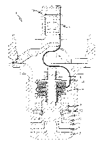
Fig. 1 is a schematic illustration of a probe unit 1 with
assembled contacting module 6. The components of the contacting
module 6 are made distinctive by double hatching. Probe unit 1
includes a probe electrode 3, which extends inwardly into the
probe housing 2 with a rod-shaped section. Probe electrode 3 is
isolated from a supplemental electrode 4 via insulation 5.
Supplemental electrode 4 coaxially surrounds the probe electrode
3. Supplemental electrode 4 is shorter than the probe electrode
3 in the direction of the housing interior, so that the probe
electrode 3 protrudes beyond the supplemental electrode 4 into
the probe housing 2. Such probe units 1 are used especially in
capacitive fill-level measuring devices. Probe electrode 3
serves, as a rule, for the actual measuring, while the
supplemental electrode 4 functions as a guard electrode. In
other words, the supplemental electrode 4 lies at the same
potential as the probe electrode 3 and improves accretion
insensitivity in the case of measuring accretion forming media.
CA 02828403 2013-08-27
Probe unit 1 can be introduced via the probe housing 2 into the
container with the medium. For this, the probe housing 2
includes, for example, a screw thread, via which it can be
screwed into the wall of the container in a receptacle with
matching thread. Probe housing 2 can serve, besides as
protection of the elements accommodated by it against
environmental influences such as condensation, also as a ground
electrode.
Probe housing 2 is sectionally tubular and includes a tapered
section, where the electrodes 3, 4 are secured. Probe electrode
3, insulation 5, supplemental electrode 4, tapered section and
an insulating unit 51 for electrical isolation between
supplemental electrode 4 and tapered section, respectively probe
housing 2, form an axial construction, wherein the longitudinal
axis of the probe housing 2 forms the axis. Located in the
probe housing 2 is a first securement means in the form of a nut
8, which is mounted on the tubular section of the supplemental
electrode 4 extending in the probe housing 2 and pulls the
section of the supplemental electrode 4 lying on the other side
of the tapered section against the tapered section. An
insulating unit 52 insulates the first nut 8 in electrically
conductive contact with the supplemental electrode 4 from the
probe housing 2. A second securement means in the form of a
second nut 9 is mounted on the rod-shaped section of the probe
electrode 3 arranged in the probe housing 2 and is tightenable
by means of a threaded engagement. Since the probe electrode 3
forms outside of the probe housing 2 the outermost element of
the axial construction, the securing of the second nut 9 effects
a tightening force directed toward the housing interior on the
11
CA 02828403 2013-08-27
elements of the axial construction and, thus, a fixed connection
of the individual elements.
The second nut 9 bears in the axial direction not only on the
supplemental electrode 4 with interpositioning of insulation,
such as would be the case when contacting the electrodes 3, 4
via solder connected cable. But here, a contacting module 6 is
arranged between the supplemental electrode 4 and the second nut
9. The second nut 9 presses the contacting module 6 against the
supplemental electrode 4. The individual elements of an
advantageous embodiment of the contacting module 6 are described
in connection with Fig. 2. Preferably located between the
contacting module 6 and the second nut 9 is a toothed washer 91.
Instead of the toothed washer 91, some other simultaneously
tightened, resilient element, or spring element, for example,
one or more Belleville springs or a helical spring, can be
mounted on the probe electrode 3. In this way, thermal
expansion effects in the axial direction are compensated,
whereby a continuous tightening force of the second nut 9 and,
thus, a lasting contact of the electrical connections produced
via the contacting module 6 are assured. The always present
compressive pressure prevents a shifting of the relative
position of contact region 71, 74 and contacting element, for
example, a contact plate 65, 66.
Via the cylindrical, basic body 64 of the insulating sleeve 62,
the contacting module 6 can in simple manner be slid onto the
probe electrode 3. Insulating sleeve 62 effects furthermore an
exact centering of the rod-shaped section of the probe electrode
3 in the tubular section of the supplemental electrode 4 and
12
,
' CA 02828403 2013-08-27
prevents damaging of the flexible circuit board 7 on the screw
thread provided in the rod-shaped section of the probe electrode
3. Additionally, the insulating sleeve 62 assures electrical
isolation of the supplemental electrode 4 from the probe
electrode 3.
The lugs 68 on the module housing 61 assure, in the case of
mounting the contacting module 6 on the probe electrode 3 a
better positionability and additionally a better holding of the
contacting module 6 upon the tightening of the second nut 9.
Because of the arising torque there would exist without the lugs
68 the danger that the module housing 61 would rotate and twist
the flexible circuit board 7. The lugs 68, which engage in
slots or cavities provided therefor in the first securement
means 8, bring about a resistance to the rotational movement, so
that the module housing 61 is locked in place and the second nut
9 is sufficiently solidly tightenable. The first nut 8 is
preferably a castellated, or slotted, nut, wherein the lugs 68
of the module housing 61 are so embodied that they engage in the
slots of the castellated, or slotted, nut. Preferably, there is
some space between module housing 61 and nut 8. Also, there is
play in the engagement of the lugs 68 in the slots of the nut 8.
The twist preventing element 67, the toothed washer 91 and the
second nut 9 are in solid contact with one another and are of an
electrically conductive material. The electrical contact
between the probe electrode 3 and the first conductive trace 72
on the flexible circuit board 7 is produced, thus, via the first
contact plate 65, the twist preventing element 67, the toothed
washer 91, and, above all, the second nut 9. The electrical
13
CA 02828403 2013-08-27
contact between the supplemental electrode 4 and the second
conductive trace 75 on the flexible circuit board 7 is produced
directly via the second contacting plate, which lies against the
end region of the supplemental electrode 4. Through the
engaging of the lugs 68, an opportunity is given for checking
that the second contact plate 66 is lying against the
supplemental electrode 4. When the second nut 9 is securely
tightened, a permanent, safe contacting is assured.
The two stage nature of the two nuts 8, 9 protects the
construction further against loosening of the nuts 8, 9, for
example, in the case of strong shakings or vibrations in a
process.
The flexible circuit board 7 is led out from the probe housing
2, so that an electronics unit can access it. To this end,
there is provided on the free (i.e. free of the insulating
sleeve 62) end region of the circuit board 7 a plug 10, which is
connectable with a corresponding counterpart of the electronics
unit. The plug 10 includes preferably sockets for contacting
the conductive traces 72, 75; it can, however, also have contact
pins. For affixing the plug 10 at a desired position, a base 11
is connected with the plug 10. For example, base 11 can engage
in a groove in the probe housing 2.
Fig. 2 shows an exploded view of an advantageous embodiment of a
contacting module 6. The insulating sleeve 62 forms the core of
the contacting module 6. Insulating sleeve 62 is composed of an
essentially cylindrical, basic body 64 and a bearing element 63,
which is washer shaped and oriented orthogonally to a surface of
14
CA 02828403 2013-08-27
the basic body 64. The cylindrical, basic body 64 is hollow, so
that it can be pushed onto the rod-shaped section of the probe
electrode 3. Bearing element 63 divides the basic body 64 into
two sections. The section, by which the insulating sleeve 62
extends into the supplemental electrode 4, is, in such case,
longer than the other section. In this way, after insertion of
the contacting module 6, the centering of the probe electrode 3
in the supplemental electrode 4 is assured.
Preferably, the insulating sleeve 62 is an injection molded or a
machined, plastic part. Bearing element 63 serves for bearing
the two contact areas 71, 74 of the flexible circuit board 7,
which are preferably likewise washer shaped. The circuit board
7 is, in such case, slid onto the insulating sleeve in such a
manner that the conductive trace 72, 75 to be contacted is
located, in each case, on that side, which faces away from the
bearing element 63. The insulating bearing element 63 located
between the two contact areas 71, 74 assures, in such case,
furthermore, that no short circuits can occur between the two
contact areas 71, 74.
Appliable against the circuit board 7 are then, respectively,
the contact plates 65, 66 mounted on the basic body 64 of the
insulating sleeve 62. In this embodiment, the first contact
region 71 is located on the short side of the basic body 64 and
the second contact region 74 on the long side. The first
contact plate 65 is mountable on the first section of the
cylindrical, basic body 64 and lies at least partially against
the first contact region 71. The second contact plate, which is
mountable on the second section of the basic body 64, is
CA 02828403 2013-08-27
advantageously embodied identically to the first contact plate
65. The contact plates 65, 66 are manufactured of an
electrically conductive material, for example, brass, copper, or
stainless steel. The shapes of the contact plates 65, 66 are
matched to the respective shapes of the contact areas 71, 74 of
the circuit board 7 and to that of the insulating sleeve 62, so
that the contact plates 65, 66 in this embodiment are likewise
washer shaped. Preferably, the contact plates 65, 66 possess in
an annular region around the central hole a greater thickness
than in the edge region. The thicker regions contact the
respectively to be contacted, conductive traces 72, 75, which in
the contact region 71, 74 are likewise ring shaped. Since the
second conductive trace 75 is led around the first conductive
trace 72 in the first contact region 71, the different
thicknesses of the first contact plate 65 assure that it only
contact the first conductive trace 72. Preferably, the contact
plates 65, 66 are symmetrical, i.e. the two side surfaces of
each have the raised portions around the center of the washer
shape.
The twist preventing element 67 is washer shaped and includes
two engagement means in the form of detents. The washer-shaped
part is insertable into the module housing 61. The detents are
embodied in such a manner that they extend out at least so far
from the module housing 61 and contact its wall or surround it
such that the twist preventing element 67 is not rotatable in
the module housing 61. Advantageously, the twist preventing
element 67 is manufactured of an electrically conductive
material. The twist preventing element 67 is not slid onto the
insulating sleeve 62, but, instead, has a central hole, whose
16
CA 02828403 2013-08-27
diameter is matched to the diameter of the probe electrode 3.
During mounting of the contacting module 6 on the probe
electrode 3, the twist preventing element 67 then contacts the
probe electrode 3 directly and not the insulating sleeve 62, so
that an electrically conductive contact between probe electrode
3 and first conductive trace 72 is produced via the twist
preventing element 67 and the first contact plate 65. The
thickness of the twist preventing element 67 is preferably
uniform.
The module housing 61 is manufactured of an insulating material,
wherein this is so selected that the insulating sleeve 62 with
the contact plates 65, 66, as well as the twist preventing
element 67 are capable of being snapped into the shell-like
module housing 61. The construction of bearing element 63,
unfolded circuit board 7 and contact plates 65, 66 is held
together by the module housing 61. For the section of the
circuit board 7, which represents the connection region between
the first contact region 71 and the second contact region 74, a
cavity is provided in the wall of the module housing 61, so that
a compression of this section of the circuit board 7 by the
module housing 61 is prevented. Furthermore, the module housing
61 has preferably at least two oppositely lying lugs 68 arranged
on its lower edge. The contacting module 6 is slid onto the
probe electrode 3 with the lower edge preceding. The lugs 68
serve, in such case, for positioning the module housing 61,
since they engage in corresponding cavities in the first
securement means 8.
17
CA 02828403 2013-08-27
In an advantageous embodiment, the upper edge of the module
housing 61 likewise has two lugs 68, so that the module housing
61 is symmetrical. The symmetry of module housing 61 and the
contact plates 65, 66 facilitates and accelerates the mounting
of the contacting module 6, since only upon the applying of the
circuit board 7 to the insulating sleeve 62 need the orientation
of the parts to be mounted be heeded.
Fig. 3 shows schematically a probe unit 1 having an alternative
form of embodiment of the contacting module 6. The second
contact plate 66 is omitted. Instead of that, the supplemental
electrode 4 contacts the second conductive trace 75 directly.
Also, the first contact plate 65 is omitted. Probe electrode 3
is electrically connected with the first conductive trace 72 via
the second nut 9, wherein the twist preventing element 67
produces the conductive contact between second nut 9 and the
first conductive trace 72. The twist preventing element 67
performs, thus, a double function as contacting aid and as
protection against twisting of the circuit board 7. In order to
enable the contacting of the first conductive trace 72, the
twist preventing element 67 is changed relative to that of the
example of an embodiment illustrated in Fig. 2 such that it has
different thicknesses in its interior region as compared with
its edge region. The outer section of the first contact area 71
is not contacted by the twist preventing element 67 because of
the smaller thickness in the edge region of the twist protection
element 67, so that the there extending, second conductive trace
75 is not contacted.
18
CA 02828403 2013-08-27
Fig. 4 shows a flexible circuit board 7 before mounting in the
contacting module 6. The circuit board 7 is essentially strip
shaped and possesses in an end region a first contact region 71
and a second contact region 74, which is connected with the
first contact region 71. The strip shaped section is here shown
shortened. The second contact region 74 can be brought to at
least partially coincide with the first contact region 71 when
the second contact region 74 is turned back 180 degrees toward
the first contact region. This also includes the case, in which
the contact areas 71, 74 have equal shape, but are, however, of
different size. The coinciding concerns, thus, essentially the
central holes. In this embodiment, the two contact areas 71, 74
are arranged one after the other. Arrangements next to one
another or at another angle are, however, likewise possible. In
order to match the washer shaped bearing element 63, the contact
areas 71, 74 are also washer shaped. The conductive traces 72,
75 in the contact areas 71, 74 are correspondingly ring-shaped.
The circular holes in the middle of the contact areas 71, 74 are
so dimensioned that the circuit board 7 is mountable via the
holes onto the insulating sleeve 62.
In this advantageous embodiment, the circuit board 7 has three
conductive traces 72, 751, 752. The first conductive trace 72
extends between the other two conductive traces 751, 752 and
terminates in the first contact region 71, where it surrounds
the circular hole with a ring-shape. The two outer conductive
traces 751, 752 can also be referred to as the second conductive
trace 75, since they both terminate in an annular structure
around the hole in the second contact region 74 and, thus, carry
the same potential. By embodying the second conductive trace 75
19
CA 02828403 2013-08-27
in the form of two tracks 751, 752 extending for the most part
parallel to one another, redundancy is created, so that the
provided electrical signal reaches the second contact region 74
even in the case of damage or a defective contacting of one of
the two tracks 751, 752. The second conductive trace 75 is led
via the edge region of the first contact region 71 to the second
contact region 74, so that the area of the first contact region
71 is somewhat greater than that of the second contact region
74. The line widths of the first conductive trace 72 and the
second conductive trace 75 are preferably essentially equal in
sections corresponding to one another.
In this embodiment, the internally lying conductive trace is
referred to as the first conductive trace 72. Thus, the contact
region, in which the internally lying conductive trace
terminates, serves for contacting the probe electrode 3.
Correspondingly, the circuit board 7, such as shown in Figs. 1-
3, is mounted on the insulating sleeve 62.
The alternative naming of the internally lying conductive trace
as the second conductive trace 75 is, however, likewise
possible, so that the contact region, in which the internally
lying conductive trace terminates, represents the second contact
region 74 for contacting the supplemental electrode 4. In this
case, the circuit board 7 is mounted correspondingly in such a
manner on the insulating sleeve 62 that the contact region, in
which the inner conductive trace terminates, is associated with
the longer section of the basic body 64 adjoining the
supplemental electrode 4 in the assembled state of the probe
unit 1.
CA 02828403 2013-08-27
Fig. 5 shows a probe unit 1 schematically. Probe unit 1 of Fig.
differs from the probe units 1 illustrated in Fig. 1 and 3
only in the lower portion, i.e. that lying below the tapered
section of the probe housing 2. The different embodiments of
the contacting module 6 can likewise be mounted in this form of
embodiment.
Probe housing 2 continues cylindrically after the tapered
section, wherein the central axis of the so formed hollow
cylinder coincides with the longitudinal axis of the probe unit
1. Also, the probe electrode 3, the supplemental electrode 4,
the insulation 5 between the two electrodes 3, 4 and the
insulating unit 51 between supplemental electrode 4 and probe
housing 2, terminate, in each case, with a cylindrical section.
The electrodes 3, 4 and insulation 5, 51 are in the radial
direction always surrounded by the cylindrical section of the
probe housing 2 and seal tightly against one another and the
probe housing 2, wherein the sealed connection is producible via
measures known to those skilled in the art. The electrodes 3,
4, insulation 5, 51 and the probe housing 2 end additionally
without offset on a shared surface. Such a probe unit 1 is
essentially installable flushly in a container. This is
especially advantageous in the case of applications, which must
fulfill high hygienic standards, since, with the flush
installation, there are less locations where bacteria can
accumulate.
21
CA 02828403 2013-08-27
List of Reference Characters
1 probe unit
2 probe housing
3 probe electrode
4 supplemental electrode
insulation
51, 52 insulating unit
6 contacting module
61 module housing
62 insulating sleeve
63 bearing element
64 basic body
65 first contact plate
66 second contact plate
67 twist preventing element
68 lug
7 circuit board
71 first contact region
72 first conductive trace
73 hole
74 second contact region
75 second conductive trace
751 outer conductive trace
752 outer conductive trace
8 first nut
9 second nut
91 toothed washer
plug
11 socket
22