Note: Descriptions are shown in the official language in which they were submitted.
CA 02829064 2013-09-04
WO 2012/120497
PCT/1L2012/000103
METHOD FOR SURFACTANT CRYSTAL GROWTH OF A
METAL-NONMETAL COMPOUND
FIELD OF THE DISCLOSED TECHNIQUE
The disclosed technique relates to crystal growth, in general,
and to methods and systems for growing crystals of a metal-nonmetal
compound using surfactants, in particular.
BACKGROUND OF THE DISCLOSED TECHNIQUE
Methods for growing crystals from a liquid melt are known in the
art. For example, US Patent No. 7,097,707, issued to Xu, entitled "GaN
boule grown from liquid melt using GaN seed wafers" is directed to
methods for making single crystal GaN boules. A first method comprises
the procedures of contacting a GaN seed wafer with a GaN source
environment under process conditions. The process conditions include a
thermal gradient in the GaN source environment for producing growth of
gallium nitride on the GaN seed wafer, thus forming the GaN boule. The
source environment can be selected from a gallium melt and a nitrogen
source or a supercritical ammonia containing solubilized GaN.
A second method comprises the procedures of providing a
gallium melt and contacting a GaN seed wafer with the gallium melt in the
presence of a nitrogen source and under a thermal gradient. This
produces the growth of gallium nitride on the GaN seed wafer, thereby
forming a GaN boule. The GaN seed wafer is attached to a rotatable rod.
The rotatable rod is rotated, thus rotating the GaN seed wafer, while
pulling the rod and the GaN seed wafer from the gallium melt during the
growth of the GaN boule. The nitrogen source comprises a nitrogen
plasma including atomic nitrogen, nitrogen ions and dinitrogen ions. Also
an ambient environment is formed of the gallium melt and the GaN seed
wafer. The nitrogen plasma is generated by a discharge technique
CA 02829064 2013-09-04
WO 2012/120497
PCT/1L2012/000103
selected from direct current discharge, radio frequency discharge and
microwave discharge. The temperature of the gallium melt is from about
900 C to about 1500 C. A GaN crust is formed on a surface of the
gallium melt, from the reaction between the nitrogen source and the
gallium melt. The thermal gradient comprises a temperature which is
higher at the GaN crust than at the GaN seed layer, whereby gallium
nitride is transported from the crust to the growth of gallium nitride on the
GaN seed wafer via dissolved atomic nitrogen in the gallium melt. The
GaN in the crust is decomposed into atomic nitrogen with an equilibrium
concentration at the temperature at the crust. The atomic nitrogen
equilibrium concentration is at supersaturation relative to the temperature
at the GaN seed wafer, thus producing homoepitaxial growth of GaN at the
seed wafer.
US Patent No. 7,892,513, issued to Fujiwara, et al., entitled
"Group III nitride crystal and method of its growth" is directed to a crystal
growth method. The method comprises the steps of preparing a substrate
having a principal face and including, at least on its principal face side, a
group III nitride seed crystal having the same chemical composition as a
group III nitride crystal. The average density of threading dislocations
along the principal face is 5x106 cm-2 or less. The method further
comprises the step of bringing a solution, in which a nitrogen containing
gas is dissolved into a group III metal containing solvent, into contact with
the principal face of the substrate, to grow the group III nitride crystal
onto
the principal face of the substrate.
SUMMARY OF THE PRESENT DISCLOSED TECHNIQUE
It is an object of the disclosed technique to provide a novel
method and system of crystal growth for growing high quality
metal-nonmetal compound crystals from a surfactant which rests above a
thin liquid metal wetting layer. In accordance with the disclosed technique,
-2-
CA 02829064 2013-09-04
WO 2012/120497
PCT/1L2012/000103
there is thus provided a method for crystal growth from a surfactant of a
metal-nonmetal (MN) compound, including the procedures of providing a
seed crystal and introducing atoms of a first metal to contact with the seed
crystal in order to form a thin liquid metal wetting layer on at least one
surface of the seed crystal. The method also includes the procedure of
setting a temperature of the seed crystal below a minimal temperature
required for dissolving MN molecules in the thin liquid metal wetting layer
and above a melting point of the first metal. Each one of the MN
molecules is formed from at least one atom of a second metal and at least
one atom of a first nonmetal. The method further includes the procedure
of introducing the MN molecules which form an MN surfactant monolayer,
thereby facilitating a formation of the thin liquid metal wetting layer
between the MN surfactant monolayer and the surface of the seed crystal.
The method finally includes the procedure of regulating a thickness of the
thin liquid metal wetting layer such that at least some of the MN molecules
of the MN surfactant monolayer couple with the surface of the seed
crystal, thereby growing an epitaxial layer of the MN compound on the
seed crystal.
In accordance with another aspect of the disclosed technique,
there is thus provided a method for crystal growth from a surfactant of a
metal-nonmetal (MN) compound, including the procedures of providing a
seed crystal and introducing atoms of a first metal in the vicinity of the
seed crystal in order to form a thin liquid metal wetting layer on at least
one surface of the seed crystal. The method also includes the procedure
of setting a temperature of the seed crystal below a minimal temperature
required for dissolving MN molecules in the thin liquid metal wetting layer
and above a melting point of the first metal. Each one of the MN
molecules is formed from at least one atom of a second metal and at least
one atom of a first nonmetal. The method further includes the procedure
of introducing the MN molecules which form an MN surfactant monolayer,
thereby facilitating a formation of the thin liquid metal wetting layer
-3-
CA 02829064 2013-09-04
WO 2012/120497
PCT/1L2012/000103
between the MN surfactant monolayer and the surface of the seed crystal.
The method finally includes the procedure of regulating a thickness of the
thin liquid metal wetting layer such that at least some of the MN molecules
of the MN surfactant monolayer couple with the surface of the seed
crystal, thereby growing an epitaxial layer of the MN compound on the
seed crystal.
In accordance with a further aspect of the disclosed technique,
there is thus provided a system for crystal growth from a surfactant of a
metal-nonmetal (MN) compound from a metal melt, including a growth
chamber, a pedestal and a motor. The pedestal is located inside the
growth chamber. The motor is coupled with the pedestal and is for moving
the pedestal in the growth chamber. A seed crystal is placed on the
pedestal such that a growth surface of the seed crystal faces opposite a
direction of the pedestal. The growth chamber is filled with the metal melt
such that the growth surface is covered by a thin layer of the metal melt. A
nonmetal gas is introduced into the growth chamber above a surface of
the metal melt. Particles of the nonmetal gas and particles of the metal
melt interact, thereby forming a MN surfactant monolayer. A distance
between the growth surface and the MN surfactant monolayer is regulated
such that molecules in the MN surfactant monolayer tunnel to the growth
surface, thereby epitaxially growing at least one crystal layer on the growth
surface.
In accordance with another aspect of the disclosed technique,
there is thus provided a system for crystal growth from a surfactant of a
metal-nonmetal (MN) compound from a thin film, including a growth
chamber, a first gas inlet and a second gas inlet. The first gas inlet is
coupled with the growth chamber and is for introducing a metal vapor into
the growth chamber. The second gas inlet is coupled with the growth
chamber and is for introducing a nonmetal vapor into the growth chamber.
A seed crystal is placed in the growth chamber. The growth chamber is
filled simultaneously with the metal vapor and the nonmetal vapor, such
-4-
= .
CA 02829064 2013-09-04
WO 2012/120497
PCT/1L2012/000103
that the metal vapor and the nonmetal vapor co-deposit on a growth
surface of the seed crystal, thereby forming a thin liquid metal wetting
layer from the metal vapor and a MN surfactant monolayer over the thin
liquid metal wetting layer. A concentration of the metal vapor is initially
higher than a concentration of the nonmetal vapor such that the thin liquid
metal wetting layer is formed. A thickness of the thin liquid metal wetting
layer is regulated such that MN molecules in the MN surfactant monolayer
tunnel to the growth surface, thereby epitaxially growing at least one
crystal layer on the growth surface.
-5-
CA 02829064 2013-09-04
WO 2012/120497
PCT/1L2012/000103
BRIEF DESCRIPTION OF THE DRAWINGS
The disclosed technique will be understood and appreciated
more fully from the following detailed description taken in conjunction with
the drawings in which:
Figure 1 is a schematic illustration of a method for growing
crystals of a metal-nonmetal compound from a surfactant, operative in
accordance with an embodiment of the disclosed technique;
Figure 2A is a first schematic illustration of the atomic structure
of a metal-nonmetal compound crystal grown using the method of Figure
1, constructed and operative in accordance with another embodiment of
the disclosed technique;
Figure 2B is a second schematic illustration of the atomic
structure of a metal-nonmetal compound crystal grown using the method
of Figure 1, constructed and operative in accordance with a further
embodiment of the disclosed technique;
Figure 2C is a third schematic illustration of the atomic structure
of a metal-nonmetal compound crystal grown using the method of Figure
1, constructed and operative in accordance with another embodiment of
the disclosed technique;
Figure 2D is a fourth schematic illustration of the atomic
structure of a metal-nonmetal compound crystal grown using the method
of Figure 1, constructed and operative in accordance with a further
embodiment of the disclosed technique;
Figure 3A is a schematic illustration of a system for growing a
metal-nonmetal compound crystal using the method of Figure 1,
constructed and operative in accordance with another embodiment of the
disclosed technique;
Figure 3B is a schematic illustration of another system for
growing a metal-nonmetal compound crystal using the method of Figure 1,
constructed and operative in accordance with a further embodiment of the
disclosed technique;
-6-
CA 02829064 2013-09-04
WO 2012/120497
PCT/1L2012/000103
Figure 4A is a schematic illustration of a crystal grown
epitaxially, constructed and operative in accordance with another
embodiment of the disclosed technique;
Figure 4B is a schematic illustration of a crystal grown epitaxially
exhibiting a Manhattan structure, constructed and operative in accordance
with a further embodiment of the disclosed technique; and
Figure 4C is a schematic illustration of a crystal grown epitaxially
exhibiting a nanowire structure, constructed and operative in accordance
with another embodiment of the disclosed technique.
-7-
CA 02829064 2013-09-04
WO 2012/120497
PCT/1L2012/000103
DETAILED DESCRIPTION OF THE EMBODIMENTS
The disclosed technique overcomes the disadvantages of the
prior art by providing a novel crystal growth method for growing high
quality metal-nonmetal compound crystals from a surfactant which rests
above a thin liquid metal wetting layer. According to the disclosed
technique, a thin liquid metal wetting layer is provided with nonmetal
atoms or metal-nonmetal particles which do not dissolve in the thin liquid
metal wetting layer. The nonmetal atoms and particles combine with metal
atoms and particles of the thin liquid metal wetting layer and adsorb on the
upper surface of the thin liquid metal wetting layer thus forming a
surfactant monolayer of metal-nonmetal molecules which includes a
specific orientation having a metallophobic side and a rinetallophilic side.
When brought in close proximity to a seed crystal which is to be grown into
a crystal, a physical mechanism enables the metal-nonmetal molecules of
the surfactant monolayer to jump, tunnel or diffuse and couple with the
seed crystal. A plurality of such jumps will form an epitaxial layer of the
metal-nonmetal molecules on the seed crystal, thus increasing its volume
and substantially growing a metal-nonmetal compound crystal on the seed
crystal. Regulating the distance between the growing seed crystal and the
upper level of the thin liquid metal wetting layer, with a continuous supply
of metal-nonmetal molecules in the surfactant monolayer, will epitaxially
grow the seed crystal into a metal-nonmetal compound crystal.
The disclosed technique relates to a general method for crystal
growth and is limited to crystals grown from compound materials. In
general, crystals grown using the disclosed technique are grown from a
precursor compound that includes at least one metal and at least one
nonmetal, herein abbreviated and referred to as an MN compound. In the
description of the disclosed technique, the term 'metal' is used to denote
any element in the periodic table of elements classified as either an alkali
metal, an alkaline earth metal, a transition metal, a lanthanide element, an
actinide element or an other metal. In the description of the disclosed
-8-
r"ririted: 0M4720:(6 PCT/IL 20 12
/0(PCl/11: 2012/0004031.3
- .1. it ..
uu. =µ; lc! =
&A, $.A./%1 I '1/4.11.J
=
003872Pc
technique, the term 'nonmetal is used to denote any element in the
periodic table of elements classified as a nonmetal or a halogen, such as
hydrogen (H), berea-(B), carbon (C), nitrogen (N), oxygen (0), Siii-60414&07
phosphorus (P), sulfur (S), afsenie--(As)7-selenium (Se), ea4imeny¨(S4
te14urn __________________________________________________ (-TOT-fluorine (F),
chlorine (Cl), bromine (Br) and iodine (I). As is
known to the worker skilled in the art the following elements in the
perioctic table of elements are classifiec as metalloids: boron (B), silicon
cS11,_germanium__(_Gel, arsenic (As), antimony (Sb), tellurium (Te) and
polonium (po). Metalloids exhibit certa!n properties which are similar to
both metals and nonmetals. As such in the description of the disclosed
technique,any element classified as a metalloid can be considered a
metal or a nonmetal depending_on which other element or elements it is
bonded. yvith.__ For example, in the com_p_ound germanium silicide_fGeSi),_
Ge acts as a metal and Si acts as a nonmetal. However in the compound
is silicon carbide (SiC_) Si acts as a metal, with C being the
nonmetal.
Examples of MN compounds that can be used as a precursor compound
include gallium nitride (GaN), alumint..m oxide (A1203), cadmium zinc
selenide (CdZnSe), indium gallium nitride (InGaN), Spinel (MgA1204),
yttrium barium copper oxide (YBa2Cu307) and the like.
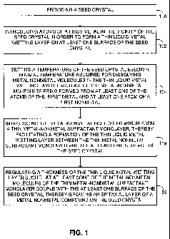
Reference is now made to Figure 1 which is a schematic
illustration of a method for growing crystals of a metal-nonmetal compound
from a surfactant, operative in accordance with an embodiment of the
disclosed technique. In a procedure 100, a seed crystal is provided. The
seed crystal represents the substrate upon which crystals of the MN
compound of the disclosed technique will be grown upon. The seed
crystal can have any kind of crystallographic structure and orientation and
is not limited in any manner. Examples of different crystallographic
structures are shown below in Figure 4A-4C. In addition, the seed crystal
= can be used to grow homogeneous crystals, where the elements
-9-
REPLACEMENT SHEET (ARTICLE 34)
Duration: 01.01.2013 16:04:31 - 01.01.2013 16:20:20. This page 8 of 24 was
completed at 01.01.2013 16:11:08
Received at the EPO on Jan 01, 2013 16:20:20. Page 8 of 24
el,f111
CA 02829064 2013-09-04 AMENDED SHEET
11-Q1-20-t3
CA 02829064 2013-09-04
Printed : 09-0422613 DESCI1AMD PCT/IL 2012
/0(PCT/IL 2012/000 10313
r i 11 'mu. V=J-i=J I i=J
I V I I I L. 4-$.0 I ea %A.A./ I %J..,
= , = =
= .
0038.12PC
comprising the seed crystal and the elements comprising the MN
compound are substantially similar. The seed crystal can also be used to
grow heterogeneous crystals, where the elements comprising the seed
crystal and the elements comprising the MN compound are substantially
5 different. The seed can further be a small crystallite which may be one
of
many polycrystalline seeds grown on an amorphous or crystalline
substrate. According to the disclosed technique, a variety of growth
environments is possible and depends upon the specific MN compound
crystal to be grown. Also, as described below the precursor materials
10 required to grow the MN compound crystals according to the disclosed
technique can be introduced in a selected growth environment using
known crystal growth methods such as chemical vapor deposition (herein
-9A-
REPLACEMENT SHEET (ARTICLE 34)
Duration: 01.01.2013 16:04:31 - 01.01.2013 16:20:20. This page 9 of 24 was
completed at 01.01.2013 16:11:32
Received at the EPO on Jan 01, 2013 16:20:20. Page 9 of 24
!WO:
/11 /1 1, rff11
2/2- AMENDED SHEET
012-012201.3
CA 02829064 2013-09-04
WO 2012/120497 PCT/1L2012/000103
abbreviated CVD), molecular beam epitaxy (herein abbreviated MBE),
liquid phase epitaxy (herein abbreviated LPE), vapor phase epitaxy (herein
abbreviated VPE) and the like. Therefore, in procedure 100, the seed
crystal which is provided is substantially placed in a suitable growth
environment, depending on the specific MN compound crystal to be grown
and the selected method for introducing the required precursor materials.
As a first example, in procedure 100, the seed crystal may be provided
and placed in a crucible for melting a 'metal, such as used in solution
growth or LPE. As a second example, in procedure 100, the seed crystal
may be provided and placed as a wafer in a high vacuum chamber, such
as used in MBE. As a third example, the seed crystal may be provided as
a polyseed layer deposited on a crystalline structure or on an amorphous
structure.
In a procedure 102, atoms of a first metal are introduced in the
vicinity of the seed crystal in order to form a thin liquid metal wetting
layer
on at least one surface of the seed crystal. In an alternative to procedure
102, atoms of a first metal are introduced to contact with the seed crystal
in order to form a thin liquid metal wetting layer on at least one surface of
the seed crystal. As mentioned above, the first metal may be similar to or
different than a metal in the seed crystal. In addition, the first metal may
be different than a metal in the seed crystal as well as a metal in the MN
crystal to be grown. In this respect, the metal forming the thin liquid metal
wetting layer may be different than both a metal in the seed crystal and a
metal in a metal-nonmetal molecule used as a precursor material for
growing an MN crystal according to the disclosed technique. In general,
the first metal might have specific attributes such as a low melting
temperature, a high evaporation temperature, being an inferior solvent of
MN molecules which are to deposit on the seed crystal as an MN crystal.
Examples of the first metal can include mercury (Hg), gallium (Ga), zinc
(Zn), tin (Sn), magnesium (Mg) and the like. Any known method in the art
may be used to introduce the atoms of the first metal in this procedure.
-10-
- .
CA 02829064 2013-09-04
WO 2012/120497
PCT/1L2012/000103
For example, the first metal atoms can be introduced as a vapor which will
eventually condense on at least one surface of the seed crystal, when the
first metal atoms are placed as a solid in a Knudsen cell which is then
heated to sublimate the first metal atoms as a vapor. The first metal
atoms can also be introduced as a liquid metal (i.e., a metal melt) which
surrounds the seed crystal on at least one of its surfaces. It is noted that
the first metal atoms may be introduced in procedure 102 as a compound,
including a metal element and a nonmetal element, in which the
compound is dissociated in the vicinity of the seed crystal thus releasing
the nonmetal atoms of the compound and condensing the first metal
atoms as a liquid on the seed crystal. It is also noted that the seed crystal
used in procedure 100 is selected such that the first metal atoms which
are introduced in the vicinity of the seed crystal, which eventually form a
thin liquid metal wetting layer on at least one surface of the seed crystal,
can exist in a liquid state on a surface of the seed crystal without
dissolving the seed crystal.
In a procedure 104, a temperature of the seed crystal is set
below a minimal temperature required for dissolving metal-nonmetal
molecules in the thin liquid metal wetting layer. This temperature can be
referred to as a liquidus temperature. As mentioned above, the disclosed
technique relates to growing MN compound crystals on a seed crystal.
Depending on the selected metal-nonmetal compound to be grown as a
crystal, the temperature of the seed crystal is set below the liquidus
temperature yet also higher than the melting point of the first metal atoms
which form the thin liquid metal wetting layer. It is
noted in one
embodiment of the disclosed technique that the metal-nonmetal molecules
referred to above are to be formed from at least one of atom of the first
metal and at least one atom of a first nonmetal. Therefore, the metal
referred to in the metal-nonmetal molecules in this procedure and the
metal which comprises the thin liquid metal wetting layer of procedure 102
are substantially the same. For
example, if gallium nitride (herein
-11-
CA 02829064 2013-09-04
WO 2012/120497
PCT/1L2012/000103
abbreviated GaN) crystals are to be grown on the seed crystal in
procedure 100, then in procedure 102, gallium (Ga) atoms are introduced
in the vicinity of the seed crystal, or are introduced to contact with the
seed
crystal, thereby eventually forming a thin liquid gallium wetting layer on a
surface of the seed crystal. In procedure 104, the temperature of the seed
crystal is set below the liquidus temperature, which is this example would
be below 1150 C. In general, it is known that MN compounds are not
easily soluble in liquid melts of the metal that forms the MN compound,
unless the MN compounds are subjected to very high temperatures and/or
very high pressures, according to their respective phase diagrams.
According to another embodiment of the disclosed technique,
the metal-nonmetal molecules referred to above are to be formed from at
least one of atom of a second metal and at least one atom of a first
nonmetal. Therefore, the metal referred to in the metal-nonmetal
molecules in this procedure and the metal which comprises the thin liquid
metal wetting layer of procedure 102 are substantially different. As noted
above, the first metal and second metal mentioned in this embodiment
may be different than the metal which constitutes the seed crystal.
According to the previous embodiment, silicon carbide (herein abbreviated
SIC) crystals, also known as carborundum, can be grown from a thin liquid
silicon wetting layer in which the seed crystal temperature is to be set
higher than 1400 C. According to this embodiment, SiC can be grown
from a thin liquid tin wetting layer in which the seed crystal temperature is
to be set at approximately 250 C. This embodiment can be used to grow
many other types of crystals such as quartz, rutile (Ti02) and the like.
In a procedure 106, molecules of a MN compound are
introduced into the growth environment of the seed crystal. The MN
compound may be introduced as molecules in which the metal and
nonmetal are already bonded. This introduction can be executed by
evaporating an MN compound, vaporizing an MN precursor or sputtering
-12-
CA 02829064 2013-09-04
WO 2012/120497
PCT/1L2012/000103
an MN compound target. The MN compound may also be introduced as
separate metal and nonmetal particles (for example, as atoms, ions,
radicals and the like) which combine in the growth environment to form MN
molecules. In it noted that in this second type of introduction, the metal
and nonmetal particles are to be co-deposited with the metal constituting
the MN molecules being the same as the first metal introduced in
procedure 102. For
example, in an additional optional procedure
occurring simultaneously as procedure 106 is executed, first nonmetal
atoms may be vaporized in the growth environment of the seed crystal
such that these first nonmetal atoms combine with the first metal atoms of
procedure 106, thus forming MN molecules and an MN surfactant
monolayer on a thin liquid metal wetting layer formed on the seed crystal.
In general, a surfactant refers to a soap-like substance that decreases the
surface tension of liquids, thereby spreading out the liquid and improving
wetting. As the MN molecules impinge upon a given surface of the seed
crystal, the MN molecules begin to form a thin metal-nonmetal surfactant
monolayer on the surface of the thin liquid metal wetting layer. In general,
the thin liquid metal wetting layer will form only if there are more metal
atoms than nonmetal atoms introduced into the growth environment. If
only MN molecules are introduced into the growth environment and
provided to the seed, vapor solid crystal growth will occur on the seed
crystal as known in the art. This MN layer is a monolayer in that it is
substantially the thickness of one molecule of the MN compound. The MN
monolayer also exhibits a two dimensional crystal-like structure in that the
monolayer includes a repeating structure of the MN molecules which
dwells on the upper surface of the thin liquid metal wetting layer and which
is substantially flat on that upper surface. The molecules in this MN layer
configure themselves to form a surfactant in which the metal atoms point
in a direction facing the thin liquid metal wetting layer and the nonmetal
atoms point in a direction facing away from the thin liquid metal wetting
layer. This is shown in greater detail below in Figures 2A-2C where the
-13-
CA 02829064 2013-09-04
WO 2012/120497
PCT/1L2012/000103
MN surfactant monolayer is shown to include a nnetallophilic side, facing a
thin liquid metal wetting layer and a metallophobic side, facing away from
the thin liquid metal wetting layer.
The MN surfactant monolayer facilitates the formation of the thin
liquid metal wetting layer which substantially forms between the MN
surfactant monolayer and the given surface of the seed crystal. In this
respect, the metal part of the MN surfactant faces into the thin liquid metal
wetting layer while the nonmetal part of the MN surfactant faces out, away
from the liquid metal wetting layer. As the temperature of the seed crystal
is set such that the MN molecules introduced will not dissolve as whole
molecules in the thin liquid metal wetting layer, the MN molecules
introduced substantially adsorb on the upper surface of the thin liquid
metal wetting layer as a surfactant monolayer. The MN surfactant
monolayer substantially flattens the thin liquid metal wetting layer.
In a procedure 108, a thickness of the thin liquid metal wetting
layer is regulated such that at least some of the MN molecules in the MN
surfactant monolayer couple with the given surface of the seed crystal,
thereby growing an epitaxial layer of a MN compound on the seed crystal.
According to the disclosed technique, if the thin liquid metal wetting layer
is substantially thin, for example, a few nanometers thick, then MN
molecules in the MN surfactant monolayer can substantially 'jump,' tunner
or 'diffuse' from the surfactant monolayer directly to the seed crystal and
couple with the seed crystal, thus growing another monolayer of the MN
compound on the seed crystal. In general, the particular thickness, or
range of thicknesses required for a MN molecule in the surfactant
monolayer to spontaneously join a crystal growing on the seed crystal is
dependent on the metal and nonmetal selected as the MN compound, the
choice of metal for the thin liquid metal wetting layer, the seed crystal
temperature as well as the energy with which the metal and nonmetal
precursor elements or compounds are introduced to the surfactant
monolayer. As such, for each type of MN compound grown as a crystal on
-14-
CA 02829064 2013-09-04
WO 2012/120497
PCT/1L2012/000103
the seed crystal, a particular thickness or range of thicknesses needs to
be regulated in this procedure to enable the MN molecules of the MN
surfactant monolayer to act as a precursor material for growing the MN
crystal on the seed crystal. If the thin liquid metal wetting layer becomes
too thin, then the wetting layer will dry up and growth of the crystal
epitaxially, layer by layer, will cease. If the thin liquid metal wetting
layer
becomes too thick, then MN molecules in the surfactant monolayer will not
be able to spontaneously 'jump,' tunner or 'diffuse' to the growing crystal
and crystal growth will cease entirely.
In procedure 108, the thickness of the thin liquid metal wetting
layer can be regulated using various techniques depending on how the
metal and nonmetal atoms which form, respectively, the thin liquid metal
wetting layer and the MN surfactant monolayer are introduced into the
growth environment. For example, if the MN molecules introduced in
procedure 106 are introduced using evaporation crucibles then the flow of
MN molecules can be regulated via an evaporation controller controlling
the rate of evaporation of the metal. Evaporation controllers in such
crystal growth environments can be embodied via an oscillating
piezoelectric quartz crystal coupled with a proportional-integral-derivative
(herein abbreviated PID) controller. If the MN molecules in procedure 106
are introduced as a plasma via at least one gas inlet, then the amount of
plasma entering the growth environment can be regulated using a gas inlet
manometer. A photo spectrometer can then be used to determine which
plasma species are present in the growth environment as well as their
relative density. Only certain plasma species will contribute to the MN
surfactant monolayer.
According to another embodiment of the disclosed technique,
regulation of the amount of plasma entering the growth environment can
be executed without the use of a gas inlet manometer and/or a photo
spectrometer. In this embodiment, a droplet criterion may be used as
follows. In general, if the MN molecules are introduced in the growth
- 1 5-
CA 02829064 2013-09-04
WO 2012/120497
PCT/1L2012/000103
environment as a plasma then a particular stoichiometric balance point
needs to be achieved between the metal and nonmetal species being
introduced in the growth environment. At this balance point, the ratio of
metal to nonmetal species is such that the thin liquid metal wetting layer is
of a thickness that enables molecules in the MN surfactant monolayer to
couple with the crystal growing on the seed crystal. In general, during
monolayer crystal growth, droplets of a particular precursor material may
form on the surface of the growing crystal. Using the example of growing
GaN crystals, Ga may be evaporated as a gas at a steady rate with
nitrogen plasma being introduced in the growth environment using a
plasmatron operating at high power. Reflection high-energy electron
diffraction (herein abbreviated RHEED) techniques can then be used to
detect an amorphous or polycrystalline material growing on the surface of
the seed crystal, which will appear on a RHEED monitor as high intensity
spots. As the power of the plasmatron is lowered, images on the RHEED
monitor will get darker as fewer spots are registered. Eventually, no spots
will be registered and at such a plasmatron power level, Ga droplets will
start to form on the surface of the seed crystal. By using trial and error,
the plasmatron power level can be further lowered and modified such that
no droplets form on the surface of the seed crystal. When no droplets
form on the surface of the seed crystal, the above mentioned balance
point is achieved such that the thin liquid metal wetting layer begins to
form on the surface of the seed crystal. Other trial and error methods are
possible for determining the proper amount of metal and nonmetal
particles for achieving the thin liquid metal wetting layer and MN surfactant
monolayer.
Referring back to procedure 104, the exact temperature which
the seed crystal is set at depends on a number of factors which can be
determined by trial and error and according to the metal and nonmetal
atoms which are selected to form the MN compound. For example, the
temperature of the seed crystal needs to be higher than the melting point
-16-
CA 02829064 2013-09-04
WO 2012/120497
PCT/1L2012/000103
of the at least one metal which is introduced in the MN compound. It is
noted that this temperature will depend on whether the metal introduced is
introduced as a pure metal or as a mixture of metals, since mixtures of
metals may have a eutectic melting point which is lower than the melting
points of the individual metals constituting the mixture. Higher
temperatures above the melting point of the metal may increase the
deposition rate of the atoms of the metal on the surface of the MN
surfactant monolayer, thus increasing the deposition rate or 'tunneling rate'
of molecules from the surfactant monolayer to the growing crystal on the
seed crystal. Even higher temperatures (although lower than the minimal
temperature described in procedure 104) may increase the tunneling rate
to such a rate that regulation of the stoichiometric balance point of the
metal and nonmetal particles forming the MN compound may be of
concern. In addition, at such higher temperatures, MN molecules forming
the surfactant monolayer may re-evaporate and MN molecules of the
grown crystal may dissociate from the current growing layer of the crystal.
Using trial and error, as is known to the worker skilled in the art, an
optimal
temperature for the seed crystal can be determined wherein the
incorporation rate of the MN molecules is maximized yet the stoichiometric
balance point of the metal and nonmetal precursor materials can be
regulated. It is also noted that trial and error may need to be used by a
worker skilled in the art to determine the rate at which the first metal atoms
and first nonmetal atoms are introduced into the growth environment (as
per procedures 102 and 106 above) since a high rate of introduction may
increase the rate at which epitaxial growth occurs on the seed crystal. At
the same time however, too high a rate of introduction may make it difficult
to maintain the stoichiometric balance point between the metal and
nonmetal precursor materials.
It is noted that the method described in Figure 1 is substantially
different than other prior art methods of crystal growth from a solution in
that the temperatures at which crystal growth is possible is significantly
-17-
CA 02829064 2013-09-04
WO 2012/120497
PCT/1L2012/000103
lower. For example, prior art methods for growing GaN crystals from a
solution usually require temperatures as high as 1400 C and a pressure
of 15000 bars, wherein according to the disclosed technique, GaN crystals
can be grown at temperatures as low as 35 C and at vacuum conditions.
Prior art methods of growing Spinel use temperatures as high as 2140 C,
whereas according to the disclosed technique, Spinel can be grown at
temperatures as low as 450 C. Growth of crystals at lower temperatures
can significantly increase the quality of the grown crystals as thermal
dislocations can occur when a crystal grown at high temperatures is
cooled to a useable temperature, such as room temperature. By reducing
the temperature difference between the growth temperature and the
useable temperature according to the disclosed technique, thermal
dislocations can be significantly reduced.
After procedure 108, an additional procedure can be executed in
which the first metal atoms of procedure 102 are no longer supplied to the
growth environment. As a result of the cessation of first metal atoms in the
growth environment, the thin liquid metal wetting layer formed in procedure
106 will dry up and the layer by layer epitaxial growth of the MN compound
crystal on the seed crystal in procedure 108 will cease. Since the
temperature of the seed crystal will still be below a temperature at which
MN molecules can dissolve in a thin liquid metal wetting layer, any crystal
growth of the metal-nonmetal compound on the seed crystal will occur
according to a vapor solid growth technique at low temperatures, as is
known in the art. Vapor solid growth of crystals on the seed crystal will
change the upper surface of the epitaxially grown MN compound crystals,
which exhibit a flat monocrystalline structure into crystals exhibiting a
polycrystalline structure. The polycrystalline structure can substantially be
considered a new seed crystal upon which the crystal growth technique of
Figure 1 can now be repeated. Therefore, after this additional procedure,
the method of Figure 1 can return to procedure 102 and epitaxial layer by
-18-
CA 02829064 2013-09-04
WO 2012/120497
PCT/1L2012/000103
layer growth of a MN compound crystal can resume again. It is noted that
in this manner different layers of MN compound crystals can be grown,
where each layer is constituted by a different metal and/or nonmetal. It is
also noted that if the original seed crystal of procedure 100 had a
pyramidal geometry, such that nanocolumns were grown from the seed
crystal, as shown below in Figure 4C, then when the polycrystalline
structure is formed in this additional procedure, the polycrystalline
structure may also exhibit a pyramidal geometry upon which additional
nanocolumns can be grown epitaxially according to the method of Figure
1. It is noted that when the thin liquid metal wetting layer is dried, the
temperature of the seed crystal as well as the rate of deposition of any
metal and/or nonmetal particles in the growth environment can be modified
to grow a particular type of polycrystalline crystal layer which buffers
between adjacent monocrystalline layers of epitaxial crystal growth. For
example, before a new thin liquid metal wetting layer is formed, a
deposition rate of a metal and/or nonmetal may be significantly increased
in order to grow a flat and thick polycrystalline crystal layer.
After procedure 108, a further procedure can be executed, either
after the aforementioned additional procedure or as an alternative to the
aforementioned additional procedure. In this further procedure, instead of
ceasing the supply of first metal atoms to the growth environment and
thereby drying up the thin liquid metal wetting layer, the supply of the first
nonmetal particles can be gradually slowed to substantially nil, thus
leaving a thin layer of the first metal atoms on the surface of the grown
crystal. This thin layer can then be evaporated by heating the seed crystal
or can be etched away using known wet chemistry or plasma chemistry
techniques. Removing this thin layer will result in a clean upper surface of
the grown crystal upon which other processes can be performed. If the
method of Figure 1 is used to grow a crystal having a Manhattan structure
or a crystal in the form of nanocolumns (respectively shown below in
Figures 4B and 4C), then after this further procedure, the upper surface of
-19-
CA 02829064 2013-09-04
WO 2012/120497
PCT/1L2012/000103
the grown crystals or nanocolumns can be cleaned by the techniques
listed above, thus leaving clean upper surfaces of the grown crystals
and/or nanocolumns. Any residue metal left between the grown crystals
and/or nanocolumns can also be removed by evaporation or via etching
using known wet chemistry or plasma chemistry techniques.
Reference is now made to Figure 2A which is a first schematic
illustration of the atomic structure of a metal-nonmetal compound crystal
grown using the method of Figure 1, generally referenced 150, constructed
and operative in accordance with another embodiment of the disclosed
technique. Figure 2A includes a solid phase 152, a thin liquid metal
wetting layer 154, an MN surfactant monolayer 156 and a gas phase 158.
In general, Figures 2A-2C show an atomic structure after procedures
100-106 (Figure 1) have been executed, i.e., after a thin liquid metal
wetting layer and a MN surfactant monolayer have been formed on top of
a seed crystal. The seed crystal may be solid phase 152 or a lower
portion of solid phase 152. Solid phase 152 represents a growing crystal
153. In this schematic illustration, a GaN crystal is shown which includes
a plurality of Ga atoms 160 and a plurality of N atoms 162. Whereas GaN
was selected as an example to illustrate the disclosed technique due to its
relatively simple structure and thus simplicity in graphic format, the general
atomic structure described in Figures 2A-2C applies to any MN compound
grown as a crystal using the method shown in Figure 1. As shown in
growing crystal 153, plurality of Ga atoms 160 and plurality of N atoms 162
are arranged in a crystallographic structure. Lower layers (not shown) of
growing crystal 153 may represent a seed crystal (not shown) upon which
growing crystal 153 was grown. As mentioned above, the seed crystal
may be homogeneous or heterogeneous with growing crystal 153. For
example, the seed crystal may be' a GaN seed, a sapphire seed or a
silicon seed. In addition, if growing crystal 153 was sapphire, then the
seed crystal may be a sapphire seed or a silicon seed. In the case that
the seed crystal and growing crystal 153 are heterogeneous, then the
-20-
CA 02829064 2013-09-04
WO 2012/120497
PCT/1L2012/000103
number of misfit dislocations due to differences in the respective
crystallographic structures of the seed crystal and the growing crystal is
substantially the reciprocal of the dimension of the seed crystal exposed to
growth. Therefore, a smaller dimension of seed crystal exposed to growth
will result in fewer misfit dislocations on the growing crystal when the two
are heterogeneous.
As described below in Figures 4A-4C, the seed crystal (not
shown) can have any suitable geometric structure that enables epitaxial
crystal growth. For example, the seed crystal may have a flat geometry in
which traditional, layer by layer epitaxy can occur, as shown here in Figure
2A-2C and below in Figure 4A. As another example, the seed crystal may
have a pyramidal geometry, as shown below in Figure 4C, from which
nanocolumns of crystals can be grown. The seed crystal can also be a
nanonneter sized crystalline seed or a bulky millimeter sized traditional
seed. The seed crystal can further be a wafer with at least one flat surface
or the tip of a crystalline fiber. It is also noted that seed crystal can be
coupled with a crystalline material (not shown) or an amorphous material
(not shown). One requirement of the seed crystal is that it does not
dissolve or melt in thin liquid metal wetting layer 154 or a metal melt (not
shown) which may surround solid phase 152. Also, any crystallographic
orientation of the seed crystal can be selected for the growth of growing
crystal 153 provided that the selected orientation is parallel to the
direction
of thin liquid metal wetting layer 154.
As described in greater detail below in Figures 3A and 3B, thin
liquid metal wetting layer 154 represents the metal which is part of the MN
crystal on the seed crystal. As shown in Figure 2A, thin liquid metal
wetting layer 154 includes a plurality of Ga atoms 160, although the Ga
atoms in thin liquid metal wetting layer 154 do not form a part of solid
phase 152. As described below in Figure 3A, thin liquid metal wetting
layer 154 can actually be a portion of a metal solution (not shown)
surrounding the seed crystal. The metal solution may be a mixture of
-21-
CA 02829064 2013-09-04
WO 2012/120497
PCT/1L2012/000103
metals. In such a case, the ratio of the constituents of the metal solution
should correspond to the molar ratio of the metal mixture to enable crystal
growth. For example, if the metal solution is a Spinel solution which only
includes the metal part of Spinel (i.e., Spinel has a chemical formula of
MgA1204, where MgAl2 represents the metal part of Spinel) then the
solution should have a molar ratio of 1 magnesium (Mg) atom to 2
aluminum (Al) atoms as per the chemical formula for Spinel. This example
shows the difference in required temperature for crystal growth of the
disclosed technique as compared with the prior art. Using a pure Spinel
solution of MgA1204 to grow crystals would require creating a Spinel melt.
The melting point of Spinel is 2135 C, thus requiring a high temperature
to create a Spinel melt and making crystal growth in such a high
temperature environment difficult. A metal mixture of magnesium and
aluminum has a eutectic melting point of 425 C, thereby enabling
significantly lower temperatures to be used to create the metal solution of
the disclosed technique. In addition, the temperature of the growth
environment also dictates the type of crucible material used, if crucibles
are used, as well as the type of heater used to generate the metal solution.
Lower temperatures enable a wider variety of crucible materials and
heaters to be used as well as being more cost effective.
In general, as described above in Figure 1, thin liquid metal
wetting layer 154 can be deposited on growing crystal 153 using a variety
of known techniques, such as vapor evaporation, MBE, CVD, VPE and the
like. Sputtering techniques can also be used to deposit thin liquid metal
wetting layer 154 on growing crystal 153 although in such techniques, care
needs to be taken regarding the purity of the thin liquid metal wetting layer
as well as its rate of deposition on growing crystal 153. As shown below in
Figures 3A and 3B, the thin liquid metal wetting layer may be a portion of a
metal melt or a thin film formed on a seed crystal or on a growing crystal.
Unlike prior art crystal growth methods, there is no requirement to dip the
-22-
CA 02829064 2013-09-04
WO 2012/120497
PCT/1L2012/000103
seed crystal, which may be a wafer, in a metal melt, although according to
some embodiments of the disclosed technique, the seed crystal may be
placed in a metal melt. In general, when atoms and particles are supplied
to the growth environment of growing crystal 153, the metal and nonmetal
atoms and particles which are precursors for growing crystal 153 are to be
co-deposited, i.e., are to be introduced into the growth environment
simultaneously. This co-deposition enables epitaxial growth of growing
crystal 153. Although not explicitly shown in Figure 2A, according to the
disclosed technique, different mixtures of metals may be introduced into
the growth environment over time, each mixture being deposited at its own
respective rate, to create a growing crystal having different layers of
constituents.
As described below in Figures 3A and 3B, growing crystal 153
may be grown using a system used for bulk crystal growth or using a
system for thin film epitaxial crystal growth. In either case, the nonmetal
constituent of growing crystal 153 comes from a gas as shown in gas
phase 158. As shown in Figure 2A, gas phase 158 includes plurality of N
atoms 162. The N atoms in gas phase 158 may actually be various
species of N particles, such as ions or radicals, depending on how the N
atoms are introduced into the growth environment. The nonmetal particles
of gas phase 158 may be supplied to the growth environment using a
variety of systems that depend on the particular nonmetal being
introduced. The nonmetal particles may either be introduced in a pure
form or as part of a mixture or compound which dissociates in the growth
environment. For example, if oxygen is to be introduced in gas phase 158,
then oxygen may be provided from an oxygen gas container. If boron is to
be introduced in gas phase 158, then decaborane may be provided which
is either activated by a plasma or cracked when it impinges on MN
surfactant monolayer 156. If carbon is to be introduced in gas phase 158,
then suitable hydrocarbons, such as methane may be provided which is
either activated by a plasma or cracked when it impinges on MN surfactant
-23-
CA 02829064 2013-09-04
WO 2012/120497
PCT/1L2012/000103
monolayer 156. Silane (SiH4) might be used as a precursor material for
introducing silicon in gas phase 158, while nonmetal elements of groups V
and VI having low melting points, such as P, As, Sb, S, Se and Te may be
introduced into the growth environment in gas phase 158 by being
evaporated from crucibles. Nitrogen may be introduced in gas phase 158
from a nitrogen gas container or as ammonia. Nitrogen may also be
introduced as nitrogen plasma or as cracked ammonia. In general, if the
nonmetal particles are introduced into gas phase 158 as a gas compound
having a relatively high temperature of dissociation, such as ammonia gas
which dissociates at around 750 C, then a radio frequency (herein
abbreviated RF) plasma or an electron cyclotron resonance (herein
abbreviated ECR) plasma can be used to supply the active nonmetal
particles. In other circumstances, the temperature of thin liquid metal
wetting layer 154 may be high enough to dissociate any gas compound in
gas phase 158. It is also noted as shown in Figure 2A, as well as in
Figures 2B and 2C, that according to the disclosed technique, growing
crystal 153 is grown in a growth environment which can be considered to
be 'metal-rich,' i.e., thin liquid metal wetting layer 154 includes more metal
particles than the nonmetal particles in gas phase 158.
As shown in Figure 2A, MN surfactant monolayer 156 forms the
upper part of thin liquid metal wetting layer 154 and represents an
interface between gas phase 158 and thin liquid metal wetting layer 154.
MN surfactant monolayer 156 includes a plurality of MN molecules which
forms a two dimensional liquid crystal above the surface of thin liquid
metal wetting layer 154. As shown in the example of Figure 2A, MN
surfactant monolayer 156 includes a plurality of GaN molecules 166,
including a first GaN molecule 168 and a second GaN molecule 170 which
are singled out for illustrative purposes in Figures 2A-2C. As shown by a
dotted line 164, plurality of GaN molecules 166 substantially flatten the
upper surface of thin liquid metal wetting layer 154 and are organized as a
self-assembled two dimensional lattice. This lattice includes only one
-24-
CA 02829064 2013-09-04
WO 2012/120497
PCT/1L2012/000103
layer of molecules, hence it is considered a monolayer. In addition,
plurality of GaN molecules 166 can 'float around' or 'wander about' MN
surfactant monolayer 156, in a similar fashion to a liquid crystal. As shown
in Figure 2A, the N atoms constituting plurality of GaN molecules 166 face
gas phase 158 whereas the Ga atoms constituting plurality of GaN
molecules 166 face thin liquid metal wetting layer 154. In this respect, as
mentioned above, plurality of GaN molecules 166 form a surfactant since
their metallophilic side, i.e., the Ga atoms, face thin liquid metal wetting
layer 154 and their metallophobic side, i.e., the N atoms, face gas phase
158.
In general, MN surfactant monolayer 156 serves two separate
functions. As an active surface agent, MN surfactant monolayer 156
lowers the surface tension of thin liquid metal wetting layer 154, thus
flattening it to resemble a 'sea' as shown in Figure 2A and enabling
epitaxial growth, as shown below in Figure 2B and 2C. In addition, as
shown below, MN surfactant monolayer 156 acts as the precursor material
for nourishing the growth of growing crystal 153. As mentioned above,
according to the disclosed technique, the distance between MN surfactant
monolayer 156 and growing crystal 153, as shown by a double headed
arrow 161, must be regulated and maintained in order to enable GaN
molecules in MN surfactant monolayer 156 to jump, tunnel or diffuse to
growing crystal 153. In addition, the thickness of MN surfactant monolayer
156 must also be regulated and maintained such that no more than two or
three monolayers (not shown) form above the surface of thin liquid metal
wetting layer 154. In
general, the aforementioned regulations are
dependent on a proper balance between the metal and nonmetal
constituents introduced into the growth environment shown in Figure 2A.
Reference is now made to Figure 2B which is a second
schematic illustration of the atomic structure of a metal-nonmetal
compound crystal grown using the method of Figure 1, generally
referenced 180, constructed and operative in accordance with a further
-25-
CA 02829064 2013-09-04
WO 2012/120497
PCT/1L2012/000103
embodiment of the disclosed technique. Similar elements in Figures 2A
and 2B are labeled using identical numbering. Figure 2B shows how first
GaN molecule 168 jumps or tunnels from MN surfactant monolayer 156 to
solid phase 152. In general, the temperature of growing crystal 153 is set
below a temperature in which thin liquid metal wetting layer 154 can
dissolve plurality of GaN molecules 166. Therefore, according to the
phase diagram (not shown) of a Ga metal melt (i.e., thin liquid metal
wetting layer 154) and GaN molecules (i.e., plurality of GaN molecules
166), GaN molecules are thermodynamically not allowed to be present in
thin liquid metal wetting layer 154. However, according to the disclosed
technique, if thin liquid metal wetting layer 154 is of a suitable thickness,
such as between one to three nanometers, then first GaN molecule 168
can jump, tunnel or diffuse from MN surfactant monolayer 156 to solid
phase 152, as shown by an arrow 182, in a similar manner to the tunneling
of electrons as is known in the theory of quantum physics. First GaN
molecule 168 may be prompted to jump or tunnel due to kinetic energy it
receives from one of plurality of N atoms 162, as shown by an arrow 184.
As the particles in gas phase 158 may have a high level of kinetic energy,
the bouncing and hitting of those particles on MN surfactant monolayer
156 may cause individual GaN molecules to jump or tunnel to solid phase
152. As growing crystal 153 is grown epitaxially, growing crystal 153 may
exhibit a stepped structure such as shown by a terrace 186 in growing
crystal 153. In general, terraces represent energy-favorable locations in a
growing crystal such that first GaN molecule 168 will be attracted to couple
with solid phase 152 specifically at terrace 186.
Reference is now made to Figure 2C which is a third schematic
illustration of the atomic structure of a metal-nonmetal compound crystal
grown using the method of Figure 1, generally referenced 200, constructed
and operative in accordance with another embodiment of the disclosed
technique. Similar elements in Figures 2A, 2B and 2C are labeled using
identical numbering. In Figure 2C, first GaN molecule 168 has coupled
-26-
CA 02829064 2013-09-04
WO 2012/120497
PCT/1L2012/000103
with solid phase 152 and joined growing crystal 153. As shown in Figure
2C, first GaN molecule 168 now has a crystallographic configuration to
match the crystallographic structure of growing crystal 153. Also shown in
Figure 2C, another GaN molecule 204 has been formed at MN surfactant
monolayer 156 and has taken the place of where first GaN molecule 168
was in Figure 2A. In addition, second GaN molecule 170 has begun to
jump and tunnel towards solid phase 152, as shown by an arrow 202.
Also, another Ga atom 206 is shown making its way to MN surfactant
monolayer 156 where it can couple with an N atom and form a further GaN
molecule to replace second GaN molecule in MN surfactant monolayer
156. Second GaN molecule 170 will be attracted to first GaN molecule
168 in growing crystal 153, as first GaN molecule is now situated at a
terrace (not labeled) in growing crystal 153. In general, once procedures
100-106 (Figure 1) are executed, procedure 108 (Figure 1) is executed
indefinitely to continuously grow layer upon layer of a crystal. As shown in
Figures 2A-2C, metal particles in thin liquid metal wetting layer 154 couple
with nonmetal particles in gas phase 158 to form MN molecules in MN
surfactant monolayer 156. The MN molecules in MN surfactant monolayer
156 then jump, tunnel or diffuse to solid phase 152, thus causing the
growth of growing crystal 153 epitaxially as precursor materials. Metal and
nonmetal particles then continue to combine into MN molecules in MN
surfactant monolayer 156 as growing crystal 153 continues to grow.
With reference back to Figure 2A, MN surfactant monolayer 156
and thin liquid metal wetting layer 154 must both be regulated and
maintained as thin layers to enable growth of the growing crystal 153
according to the disclosed technique. Thin liquid metal wetting layer 154
should not have a thickness greater than three nanometers and MN
surfactant monolayer 156 should include not more than two to three
monolayers, each having a thickness of approximately 0.3 nanometers. In
general, the closer MN surfactant monolayer 156 is to growing crystal 153,
the easier it should be for plurality of GaN molecules 166 to tunnel to
-27-
CA 02829064 2013-09-04
WO 2012/120497
PCT/1L2012/000103
growing crystal 153 and the frequency at which GaN molecules jump and
couple with solid phase 152 should increase. As the distance between the
upper layer (not labeled) of solid phase 152 and MN surfactant monolayer
156 increases, fewer GaN molecules will tunnel to solid phase 152. In
addition, particles in gas phase 158 may combine with particles in thin
liquid metal wetting layer 154 to form additional layers of metal-nonmetal
molecules on MN surfactant monolayer 156. For example, the thickness
of MN surfactant monolayer 156 may increase to two or three monolayers
(not shown in Figures 2A-2C) in this manner in which case it would be a
MN surfactant layer. It is assumed that at such a thickness of two or three
monolayers, the surfactant layer will still be elastic enough to form a stable
two dimensional liquid crystal and that molecules in the surfactant layer
can still tunnel to solid phase 152.
However, if the thickness of the surfactant layer were to further
increase, such as being four monolayers or greater, then the surfactant
layer may become unstable with crystallization spots appearing along the
surfactant layer. Such crystallization spots may appear in order to relieve
any stresses in the surfactant layer caused by uncommon angles formed
between molecules in the surfactant layer. These crystallization spots
may be relatively short in distance and may form non-right angles between
adjacent atoms and molecules in the surfactant layer. This in turn may
lead to an increase in density of atoms and molecules in selected portions
of the surfactant layer which may lead to avalanche crystallization. The
surfactant layer may then get stiffer, flaws may appear in its structure and
it may ultimately break. A polycrystalline layer embedded with droplets
may then appear at the level of the surfactant layer which may cease
epitaxial growth of growing crystal 153. Related consequences are
assumed as well regarding the thickness of thin liquid metal wetting layer
154. If thin liquid metal wetting layer 154 becomes too thick, since too
many metal particles were introduced into the growth environment, then
epitaxial growth of growing crystal 153 from molecules in the surfactant
-28-
CA 02829064 2013-09-04
WO 2012/120497
PCT/1L2012/000103
layer may cease and the surfactant layer may turn into a polycrystalline
layer as mentioned above. In addition, if thin liquid metal wetting layer 154
becomes too thin, epitaxial growth of growing crystal 153 may cease due
to a drying of thin liquid metal wetting layer 154. As mentioned above, the
thicknesses of both thin liquid metal wetting layer 154 and MN surfactant
monolayer 156 need to be regulated to ensure that epitaxial growth of
growing crystal 153 from molecules in the surfactant layer continues.
It is also noted that MN surfactant monolayer 156 may serve an
additional function of preventing the formation of droplets on growing
crystal 153. In prior art crystal growing methods where crystals are grown
using vapor-solid growth techniques, metal vapor deposited on a wafer or
substrate causes the formation of droplets on the wafer or substrate
surface which can lead to defects in the grown crystal. According to the
disclosed technique, MN surfactant monolayer 156 substantially forms as
thin liquid metal wetting layer 154 is formed. MN surfactant monolayer
156 acts as an active surface agent which neutralizes the surface energy
of thin liquid metal wetting layer 154 and thus prevents the formation of
droplets. This is due to the amphiphilic nature of the molecules forming
MN surfactant monolayer 156. Unlike prior art methods of thin film epitaxy
where droplets are expected during the growth process and steps need to
then be taken once droplets form in order to eliminate them, according to
the disclosed technique the formation of droplets is avoided due to the
presence of the MN surfactant layer. The metal and nonmetal particles
substantially form the molecules of the surfactant layer which substantially
prevents the formation of droplets.
Regarding gas phase 158, it is noted that a mixture of gases
may be supplied to gas phase 158 thus forming different constituents and
precursor materials in MN surfactant layer 156 for growing crystal 153.
Thus different materials may constitute the various layers of growing
crystal 153. It is understood however by the worker skilled in the art that
different mixtures of gases will have different levels of efficiency in
-29-
CA 02829064 2013-09-04
WO 2012/120497
PCT/1L2012/000103
incorporating MN molecules, formed from the mixtures of gases, into
growing crystal 153. Different mixtures of gases may also affect the ease
at which MN molecules can jump and tunnel into solid phase 152.
Reference is now made to Figure 2D which is a fourth schematic
illustration of the atomic structure of a metal-nonmetal compound crystal
grown using the method of Figure 1, generally referenced 210, constructed
and operative in accordance with a further embodiment of the disclosed
technique. Figure 2D includes a solid phase 212, a thin liquid metal
wetting layer 214, an MN surfactant monolayer 216 and a gas phase 218.
Figure 2D shows an atomic structure after procedures 100-106 (Figure 1)
have been executed, i.e., after a thin liquid metal wetting layer and a MN
surfactant monolayer have been formed on top of a seed crystal in which
the metal constituting the thin liquid metal wetting layer is different than
the
metal in the MN surfactant monolayer. Solid phase 212 represents a
growing crystal 211. In this schematic illustration, a SiC (silicon carbide)
crystal is shown which includes a plurality of Si (silicon) atoms 213 and a
plurality of C (carbon) atoms 215. As shown in growing crystal 211,
plurality of Si atoms 213 and plurality of C atoms 215 are arranged in a
crystallographic structure. As shown, thin liquid metal wetting layer 214
includes a plurality of Sn (tin) atoms 217. MN surfactant monolayer 216
includes a plurality of SiC molecules 220 arranged in a two dimensional
crystallographic orientation as a surfactant, as shown by a line 222. Gas
phase 218 includes a plurality of SiC molecules 224.
The atomic structure shown in Figure 2D can be prepared as
follows. Solid phase 212 may be a SiC wafer seed. The SiC wafer seed
is introduced into a radio frequency (herein abbreviated RF) spuftering
reactor (not shown). An argon plasma (not shown) is then used to clean
the upper surface (not labeled) of the SiC wafer seed while the
temperature of the SiC wafer seed is raised to 250 C. ft is noted that this
temperature is above the melting point of Sn yet below the liquidus
temperature of SiC such that SiC molecules will not dissolve in the tin
-30-
CA 02829064 2013-09-04
WO 2012/120497
PCT/1L2012/000103
wetting layer. By biasing the SiC sputtering target with RF waves, argon
atoms will sputter SiC molecules off the SiC sputtering target, shown as
plurality of SiC molecules 224. Simultaneously, a tin effusion cell (not
shown), coupled with the RF sputtering reactor, is opened such that tin
vapor (not shown) is emitted for long enough, for example for a minute,
such that thin liquid metal wetting layer 214 forms on the surface of solid
phase 212. Thin liquid metal wetting layer 214 may have a thickness of
approximately one nanometer. As mentioned above, the wetting layer is a
thin liquid tin wetting layer. A portion of plurality of SiC molecules 224
adsorb on the upper surface of thin liquid metal wetting layer 214, thereby
flattening plurality of Sn atoms 217 and forming MN surfactant monolayer
216, shown as plurality of SiC molecules 220. As shown in Figure 2D,
each one of plurality of SiC molecules 220 has its metallophilic side,
constituting plurality of Si atoms 213, facing plurality of Sn atoms 217, and
its nrietallophobic side, constituting plurality of C atoms 215, facing gas
phase 218.
Without changing the sputtering conditions of the RF sputtering
reactor, SiC molecules in gas phase 218 will knock and impinge upon
plurality of SiC molecules 220 which are part of MN surfactant monolayer
216. SiC molecules in MN surfactant monolayer 216 which are knocked
into thin liquid metal wetting layer 214 may jump, tunnel or diffuse to solid
phase 212, thus joining growing crystal 211, such as a SiC molecule 219,
which has already joined growing crystal 211, or a SiC molecule 221,
which is en route to joining growing crystal 211, as shown by an arrow
223. Once a SiC molecule leaves MN surfactant monolayer 216, a SiC
molecule in gas phase 218 may take its place in MN surfactant monolayer
216.
Reference is now made to Figure 3A which is a schematic
illustration of a system for growing a metal-nonmetal compound crystal
using the method of Figure 1, generally referenced 230, constructed and
operative in accordance with another embodiment of the disclosed
-31-
CA 02829064 2013-09-04
WO 2012/120497
PCT/1L2012/000103
technique. System 230 includes a growth chamber 232, a pedestal 234
and a motor 236. Motor 236 is coupled with pedestal 234. Growth
chamber 232 may be a crucible. Motor 236 can lower and raise pedestal
234 in growth chamber 232, for example as shown by an arrow 248, motor
236 can lower pedestal 234. Motor 236 can also rotate pedestal 234 (not
shown in Figure 3A). System 230 represents a system for growing bulk
crystals from a bulk liquid metal. A seed crystal 238 is placed on pedestal
234. Seed crystal 238 may be itself be placed on a substrate (not shown)
which is placed on pedestal 234. Seed crystal 238 is placed on pedestal
234 such that a surface 250 upon which crystals are to be grown is facing
an opposite direction of pedestal 234. Growth chamber 232 is filled with a
metal melt 240 such that metal melt 240 covers surface 250. Many known
techniques can be used for filling growth chamber 232 with metal melt 240
and for continuously supplying metal melt 240 to growth chamber 232. It
is noted that if growth chamber 232 is embodied as a crucible then the
material of growth chamber 232 needs to be properly selected to contain
metal melt 240 such that metal melt 240 will not dissolve the crucible at
the melting temperature of metal melt 240.
A nonmetal gas 242 is then provided to growth chamber 232
above the surface of metal melt 240. Particles of nonmetal gas 242 and
metal melt 240 will interact thereby forming a metal-nonmetal surfactant
monolayer 246 above surface 250 of seed crystal 238. MN surfactant
monolayer 246 substantially flattens the upper layer of metal melt 240. As
shown in Figure 3A, the distance between surface 250 and MN surfactant
monolayer 246, shown as a line 244, is regulated to be within a few
nanometers such that MN molecules in MN surfactant monolayer 246
jump and tunnel to surface 250 and begin forming a crystal on seed crystal
238. The distance as shown by line 244 can be regulated by lowering or
raising pedestal 234 as well as by regulating the amount of metal melt 240
supplied to growth chamber 232. For example, pedestal 234 can be
lowered at a rate which corresponds to the rate at which MN molecules
-32-
CA 02829064 2013-09-04
WO 2012/120497
PCT/1L2012/000103
from MN surfactant monolayer 246 join surface 250 of seed crystal 238
and grow a crystal (not shown) epitaxially, thereby maintaining the
distance shown by line 244.
System 230 can be used to grow bulk crystals which have
substantially no defects as only the surface of seed crystal 238 which
faces MN surfactant monolayer 246 is used to grow crystals. For
example, suppose system 230 is used to grow single GaN crystals. In
such an example, metal melt 240 will be a gallium melt and nonmetal gas
242 will be nitrogen gas or a nitrogen plasma. Seed crystal 238 will be a
defectless nanopillar having at least two types of surfaces, a first type of
surface referred to as an m-plane and a second type of surface referred to
as a c-plane. A surface 250 represents one of six m-planes of seed
crystal 238 whereas a surface 252 represents one of two c-planes of seed
crystal 238 which may be a nanopillar. In this example, the seed crystal is
placed on pedestal 234 such that one of its m-planes is parallel to MN
surfactant monolayer 246. GaN strip crystals can then be grown on that
m-plane of seed crystal 238. The thin strip of crystals grown on one of the
m-planes of the nanopillar can then be rotated 90 degrees and growth can
continue on one of the c-planes of the seed crystal. The above described
procedures can be repeated at desired planes of the seed crystal until a
sufficiently large seed crystal is attained. Depending on the amount of
time GaN crystals are grown on seed crystal 238 on one of its m-planes, a
single GaN crystal which is substantially defect free can be grown.
Placing this square sheet of single GaN crystals on one of its c-planes, a
substantially endless bulk of GaN crystals can then be grown. As
mentioned above, the temperatures of seed crystal 238 and metal melt
240 are below the minimum temperature required for dissolving GaN
molecules in a Ga melt, therefore according to this example, bulk GaN
crystals can be grown at a substantially low temperature as compared with
prior art techniques for growing bulk GaN crystals, for example at 300 C.
-33-
CA 02829064 2013-09-04
WO 2012/120497
PCT/1L2012/000103
Reference is now made to Figure 3B which is a schematic
illustration of another system for growing a metal-nonmetal compound
crystal using the method of Figure 1, generally referenced 260,
constructed and operative in accordance with a further embodiment of the
disclosed technique. System 260 includes a growth chamber 262, a first
gas inlet 264 and a second gas inlet 266. Growth chamber 262 may be a
high vacuum growth chamber. System 260 represents a system for
growing crystals from a thin film, also known as thin film epitaxy. A seed
crystal 272 is placed in growth chamber 262. Seed crystal 272 may itself
be placed on a substrate (not shown) which is placed in growth chamber
262. Growth chamber 262 is filled simultaneously with a metal vapor,
shown by an arrow 268 and a nonmetal vapor, shown by an arrow 270.
Metal vapor 268 and nonmetal vapor 270 co-deposit on the upper surface
(not labeled) of seed crystal 272, thereby simultaneously forming a thin
liquid metal wetting layer 274 and an MN surfactant monolayer 276
including metal-nonmetal molecules formed from metal vapor 268 and
nonmetal vapor 270. According to the disclosed technique, the MN
molecules in MN surfactant monolayer 276 tunnel towards the surface of
seed crystal 272 thereby growing a MN crystal on seed crystal 272.
Known methods can be used to regulate the amount of metal vapor 268
and nonmetal vapor 270 in growth chamber 262. In general, according to
the disclosed technique, the concentration of metal vapor 268 at the start
of growth procedures used in system 260 should be higher than the
equivalent concentration of nonmetal vapor 270 in growth chamber 262,
such that thin liquid metal wetting layer 274 is formed. For example, if a
one nanometer thick liquid metal wetting layer is desired then an additional
metal deposition rate of 0.1 angstroms per second for 100 seconds needs
to be supplied at the start of the growth procedures. Thereafter a
stoichiometric balance point between the metal vapor and the nonmetal
vapor can be returned to. As mentioned above, the thickness of thin liquid
metal wetting layer 274 needs to be regulated such that its remains
-34-
CA 02829064 2013-09-04
WO 2012/120497
PCT/1L2012/000103
generally constant as per the disclosed technique during crystal growth.
As is known to those skilled in the art, at high temperatures thin liquid
metal wetting layer 274 may slowly return to a vapor state, therefore any
loss in thickness of thin liquid metal wetting layer 274 must be
compensated for by an incremental addition of metal vapor 268 to growth
chamber 262.
Reference is now made to Figure 4A which is a schematic
illustration of a crystal grown epitaxially, generally referenced 300,
constructed and operative in accordance with another embodiment of the
disclosed technique. Figure 4A shows how crystals grown according to
the disclosed technique grow in monolayers in which individual molecules
couple with a growing crystal. Figure 4A shows a crystal (not labeled)
being grown epitaxially in four different stages. The four different stages
are labeled sequentially 302A, 302B, 302C and 302D. Each crystal is
shown as being comprised of a plurality of squares 304, where each
square 304 represents a repeated pattern in the composition of the crystal.
Each square 304 may represent a molecule which couples with the crystal.
As shown in stage 302A, the crystal exhibits a terrace 306 which is an
energy favorable site for a molecule to couple with the crystal and in
particular to tunnel from a surfactant monolayer (not shown) to the crystal.
In stage 302B, a molecule 308 has coupled with the crystal at terrace 306.
In stage 302C, a molecule 310 has coupled with the crystal at the next
available terrace (not labeled). In stage 302D, a molecule 312 has
coupled with the crystal at the next available terrace (not labeled). As
shown, the crystal is formed molecule by molecule as molecules in the
surfactant monolayer tunnel towards the surface of the growing crystal.
This enables a crystal to grow epitaxially with substantially no defects.
Reference is now made to Figure 4B which is a schematic
illustration of a crystal grown epitaxially exhibiting a Manhattan structure,
generally referenced 330, constructed and operative in accordance with a
further embodiment of the disclosed technique. Figure 4B shows a crystal
-35-
CA 02829064 2013-09-04
WO 2012/120497
PCT/1L2012/000103
(not labeled) being grown epitaxially in three different stages. The three
different stages are labeled sequentially 332A, 332B and 332C. Each
crystal is shown as being comprised of a plurality of squares 346, where
each square 346 represents a repeated pattern in the composition of the
crystal. Each square 346 may represent a molecule which couples with
the crystal. As shown in stage 332A, the crystal includes a plurality of
peaks 334 and a plurality of troughs 336. The crystal can be etched or
scribed using known techniques to give it the structure shown in stage
332A. According to the disclosed technique only sections of the crystal
which are substantially close to an upper level of a thin liquid metal wetting
layer (not shown) will continue to grow by molecules tunneling from a
surfactant monolayer (not shown). In stage 332B, a plurality of peaks 340
has grown another molecule high whereas a plurality of troughs 338 has
not since plurality of troughs 338 are too far from the upper level of the
thin
liquid metal wetting layer to have a molecule tunnel to the crystal at that
section. In stage 332C, a plurality of peaks 342 has grown a further
molecule high whereas a plurality of troughs 344 has not since plurality of
troughs 344 are too far from the upper level of the thin liquid metal wetting
layer to have a molecule tunnel to the crystal at that section. As
mentioned above, the thin liquid metal wetting layer is regulated to be
slightly above the top of plurality of peaks 334, 340 and 342. As shown
clearest in stage 332C, the disclosed technique enables a crystal to be
grown to form a Manhattan structure which includes a plurality of high
peaks, or thin walls, interspersed by a plurality of open vias or 'streets.'
The crystal of Figure 4B may exhibit a mesa structure (not shown).
Reference is now made to Figure 4C which is a schematic
illustration of a crystal grown epitaxially exhibiting a nanowire structure,
generally referenced 360, constructed and operative in accordance with
another embodiment of the disclosed technique. Figure 4C shows a
substrate 361 upon which a plurality of seed crystals 364 are grown.
Figure 4C shows three different stages of growth, sequentially labeled
-36-
CA 02829064 2013-09-04
WO 2012/120497
PCT/1L2012/000103
362A, 362B and 362C. Substrate 361 may be crystalline or amorphous in
structure, while plurality of seed crystals 364 is crystalline in structure.
Substrate 361 initially exhibits a pyramidal geometry, as shown in stage
362A, where a plurality of short pyramids are shown representing plurality
of seed crystals 364. Substrate 361 can be etched or scribed to generate
the seed crystal geometry shown in stage 362A. According to the
disclosed technique, the plurality of short pyramids represents an energy
favorable site for molecules from a surfactant monolayer (not shown) to
join plurality of seed crystals 364. The entire upper surface of substrate
361 is covered by a thin liquid metal wetting layer (not shown) yet only the
peaks of plurality of seed crystals 364 will grow as they are the closest to a
surfactant monolayer (not shown) which rests on top of the thin liquid
metal wetting layer. As shown in stages 362B and 362C, plurality of seed
crystals 364 has grown into a plurality of nanowires 366 and 368
respectively, wherein regulation of the thin liquid metal wetting layer
encourages molecules from the surfactant monolayer to only couple with
the peaks of the plurality of short pyramids. As in Figure 4B, the growth of
the peaks of the plurality of short pyramids leaves a plurality of
interspersed troughs (not labeled) or open vias.
With reference back to Figures 1 and 2A-2C, the disclosed
technique provides for a number of novel uses and crystal structures that
can be grown. For example, the disclosed technique can be used to grow
a monocrystalline structure on non-regular substrates, such as substrates
that exhibit curved or rounded surfaces. The method of Figure 1 can be
used with an intermediate pressure CVD growth chamber to grow epitaxial
layers on curved surfaces like crystalline fibers or seeded optical quartz
crystal fibers as a uniform pressure will exist throughout the CVD growth
chamber including the curved surfaces. Using the method of Figure 1, on
a crystalline fiber, a selected metal sheet co-deposited with a nonmetal
component can be grown for wetting the surface of the crystalline fiber
(procedures 102 and 104, both of Figure 1). Thereafter, by modifying the
-37-
CA 02829064 2013-09-04
WO 2012/120497
PCT/1L2012/000103
rate of deposition of the selected metal a stoichiometric balance point for
the growth of a buffering surfactant layer can be achieved (procedure 106
of Figure 1), thus enabling epitaxial layer by layer growth of a crystal on
the crystalline fiber. As another example, a YBa2Cu307 high temperature
(herein abbreviated HTc) superconductor can be grown on a sapphire
crystalline fiber using the disclosed technique at a low temperature, as the
metal mixture of Y (yttrium), Ba (barium) and Cu (copper) may have a
relatively low eutectic melting point. As a further example, in the case of
quartz fibers, a seed layer can be grown on a quartz fiber at vapor solid
conditions without a metal sheet. Then, using the method of Figure 1, a
metal deposition rate can be increased to higher than a stoichiometric
balance point thus forming a metal sheet and metal wetting layer on the
seed layer. Afterwards, the metal deposition rate can be reduced to the
stoichiometric balance point thus enabling nanocolumns to grow and
extend out of the quartz fiber in a radial direction.
As mentioned above, the disclosed technique enables crystals
exhibiting a monocrystalline structure to be grown at significantly lower
temperatures that prior art methods for monocrystalline growth. The
growth temperature used in the disclosed technique can in principle be
only slightly higher than the melting temperature of the metal or metal
mixture introduced in procedure 102 (Figure 1). For example, sapphire,
which is an aluminum oxide crystal, is grown using the prior art
Czochralski method at 2050 C while according to the disclosed technique
can be grown at 680 C.
In addition, the disclosed technique enables only a specific plane
of a seed crystal to be grown such that a particular crystallographic
orientation of growth can be selected. As explained above in Figures
2A-2C, the precursor material for crystal growth according to the disclosed
technique is substantially MN molecules in an MN surfactant monolayer
which is situated at a relatively close distance to the surface of a seed
-38-
CA 02829064 2013-09-04
WO 2012/120497
PCT/1L2012/000103
crystal. Therefore, only the plane of the seed crystal which is relatively
close to the MN surfactant monolayer will undergo crystal growth
according to the disclosed technique. In prior art methods of crystal
growth, like crystal growth from a metal melt or crystal growth from a
solution, a seed crystal is immersed in a liquid such that precursor
molecules approach the seed crystal from all sides. In these prior art
methods, the crystal grows according to the natural, thermodynamically
prescribed growth rate of each surface or plane of the seed crystal. Using
the disclosed technique, reactive precursor molecules are
thermodynamically not allowed to approach the growing crystal from any
side except for the side, or plane that is in close proximity to the
surfactant
monolayer. This difference enables specific planes of a crystal to be
grown which may be useful for specific crystal applications. For example,
the m-plane of GaN is particularly useful in the construction of transistors
since it does not exhibit any piezoelectric properties which can attract high
electrical fields that are detrimental for carrier mobility. According to the
disclosed technique, a seed crystal can be cut and prepared in such a way
that the desired plane, such as the m-plane in GaN, will be parallel and in
close proximity to the surfactant monolayer. In the case of prior art MBE
methods for crystal growth, even though precursor materials are supplied
from only one direction and crystals are grown in that specific direction,
when nanocolumns are grown using known MBE methods, approaching
metal atoms can couple with the growing crystal indiscriminately and can
deposit between the nanocolumns in the troughs. This may result in side
crystal growth as well as in a thickening of the nanocolumns. Very high
temperatures may avoid this issue in these prior art MBE methods.
According to the disclosed technique, crystal growth in the troughs of
nanocolumns is avoided, even at lower temperatures, since the precursor
materials only deposit on the upper surface of the nanocolumns that are in
close proximity to the surfactant monolayer.
-39-
CA 02829064 2013-09-04
WO 2012/120497
PCT/1L2012/000103
The disclosed technique enables crystals to be grown at ideal
conditions for high quality crystals having substantially no defects or
dislocations. In general, crystal growth in a liquid is substantially calmer
and less temperature dependent than other methods of crystal growth,
such as MBE, since approaching precursors molecules can drift and float
on the crystalline surface of the growing crystal to an optimal site for their
incorporation into the growing lattice of the crystal structure. This optimal
placement of precursor materials in the growing lattice results in high
quality monolayers of crystal growth and thus ultimately in a superior
crystal. The disclosed technique enables crystals to be grown in a liquid,
as described above, as well as to be grown in an environment where a
stoichiometric balance point is achieved between the precursor materials.
In general, a stoichiometric balance point is more easily achieved in a
liquid, as provided by the disclosed technique. As is known, highest
quality electro-optical GaN films and nanocolumns are grown in
gallium-rich environments which can be better controlled in a liquid growth
environment.
Also according to the disclosed technique, complex alloys can
be used in crystal growth and grown crystals can also be doped. For
example, ternary alloys such as indium gallium nitride and cadmium zinc
selenide can be used as precursor materials for crystal growth at low
temperatures since metal mixtures tend to have low eutectic melting
points. The nonmetal atoms and particles used as a precursor material
can also be complex according to the disclosed technique, such as gallium
phosphor arsenide or zinc oxide telluride. As such, the disclosed
technique provides for a method of crystal growth using very uncommon
metal and nonmetal compounds. Furthermore, the proximity of the
precursor materials to the growing surface of the crystal makes it much
easier to dope the growing surface, which may be a semiconductor film,
with n-type or p-type impurities. In addition, doping the growing surface at
low temperatures substantially reduces the thermal budget of the crystal
-40-
CA 02829064 2013-09-04
WO 2012/120497
PCT/1L2012/000103
which normally causes a high diffusion distance of the dopants and also
affects the desired concentration of the dopants.
According to another embodiment of the disclosed technique,
different layers in a grown crystal can include different compositions as
well as different gradients or transitions of precursor materials from one
layer to the next. For example, a seed crystal of A1203 (aluminum oxide)
can be used to grow a first layer of AIN (aluminum nitride) followed by a
second layer of GaN using the disclosed technique. Each layer may be
transitioned to another layer by controlling the deposition rate of each
metal, thus the AIN layer may be gradually transitioned to the GaN layer or
may be transitioned in a sharp manner by changing the deposition rate of
aluminum or gallium. In
general, the only restriction regarding this
embodiment of the disclosed technique is that the various layers grown
should have a similarity in lattice structure thereby avoiding misfit
dislocations in the grown crystal. In accordance with this embodiment, the
surfactant monolayer which serves as the precursor material for crystal
growth can be gradually altered to enable the growth of thin films with a
graded composition. The metal and nonmetal precursor materials which
constitute the surfactant monolayer can be altered by changing the
deposition rate of each. Such thin films with a graded composition may be
used to construct a graded direct bandgap semiconductor. Such a
semiconductor may be used to collect solar energy over a wide spectrum
of solar emissions where each color present in a solar emission is
collected by a layer in the semiconductor having a corresponding
bandgap. Examples of such layers may include monolayers having
generalized formulas such as InxGai_xN, AlxGai_xAs, GaAsxN1_, and the
like. In other embodiments of the disclosed technique, the various layers
grown should have a similarity in lattice structure yet misfit dislocations
may be encouraged in order to grow nanocolumns.
The disclosed technique further enables uncommon crystal
structures to be grown at low and steady temperatures. For example,
-41-
CA 02829064 2013-09-04
WO 2012/120497
PCT/1L2012/000103
when depositing InGaN (indium gallium nitride) by MBE methods, care has
to be taken regarding the growth temperature of the system since GaN
dissociates at 800 C whereas InN (indium nitride) dissociates at 550 C.
At low temperatures, epitaxy will not occur whereas at high temperatures
InN will not be incorporated into a growing lattice since it will dissociate.
Using the disclosed technique, InGaN can be grown at 50 C. Therefore,
according to the disclosed technique, new precursor materials not
considered for crystal growth may be used in crystal growth as
temperature incompatibilities of certain alloys and mixtures can be
avoided.
The disclosed technique also enables heterocrystalline
structures to be grown, as the disclosed technique can be used to grow
crystals heteroepitaxially. For
example, regarding thin film growth
systems, as shown above in Figure 3B, a thin liquid metal wetting layer
can be provided with various types of nonmetal particles at different times,
such as first nitrogen, then phosphorus and finally arsenide. The varying
nonmetal particles will change the composition of the surfactant monolayer
which in turn will change the composition of the grown crystal, thus
enabling heteroepitaxy. As another example, the thin liquid metal wetting
layer of a given metal can be dried according to the disclosed technique
and a new thin liquid metal wetting layer, composed of a different metal,
can then be deposited on the growing crystal. Alternatively, different
metals can be introduced into the growth environment while the thin liquid
metal wetting layer is being deposited on the seed crystal to enable
heteroepitaxy. As mentioned above, various layers of crystal growth
grown on the seed crystal can be dried upon which new layers of crystals
can be grown or a given crystal layer can have its composition changed by
changing the precursor MN molecules of the surfactant monolayer.
As described above in Figures 4B and 4C, the disclosed
technique enables novel structures of crystals to be grown, such as
-42-
CA 02829064 2013-09-04
WO 2012/120497
PCT/1L2012/000103
nanocolumns or Manhattan structures. Using prior art crystal growth
techniques, when precursor materials in a liquid or gas state are deposited
as a thin film on a seed crystal having a non-flat surface, the thin film
usually conforms to the topology of the non-flat surface and results in a
non-flat grown crystal. As described above, MBE methods and CVD
methods can result in crystal growth exhibiting a pyramidal geometry and
can lead to the growth of nanocolumns although as more atoms and
particles are deposited using such methods, any nanocolumns grown start
to thicken and troughs between grown nanocolumns begin to fill up.
According to the disclosed technique, troughs between grown
nanocolumns are kept clean of particle deposits since precursor molecules
will only jump or tunnel to adjacent surfaces in the vicinity of the
surfactant
monolayer.
It will be appreciated by persons skilled in the art that the
disclosed technique is not limited to what has been particularly shown and
described hereinabove. Rather the scope of the disclosed technique is
defined only by the claims, which follow.
-43-