Note: Descriptions are shown in the official language in which they were submitted.
CA 02829331 2013-08-14
WO 2012/109724
PCT/CA2011/000154
3D MICROFLUIDIC DEVICES BASED ON OPEN-THROUGH THERMOPLASTIC
ELASTOMER MEMBRANES
Field of the Invention
The present invention is related to open-through thermoplastic elastomer (TPE)
membranes, to methods of producing open-through TPE membranes and to three-
dimensional microfluidic devices based on such membranes.
Background of the Invention
The accurate deposition and patterning of biological probes on a solid support
is
of critical importance to numerous bioassays. For
example, protein and DNA
microarrays, which offer the interesting possibility to study concurrently the
interaction
between a target sample and a large number of different biological probes,
have become
key components of drug discovery, clinical diagnostics, and gene sequencing.
However,
microarrays still largely depend on detection techniques such as fluorescence
labeling or
surface plasmon resonance which are difficult to apply in point-of-care
applications.
Recently, new detection techniques involving integrated sensors with
microfabricated
biosensing elements have emerged, including: nanowires, field-effect-
transistors, optical
sensing waveguides, and electrochemical sensors. This new
generation of
microfabricated biosensor arrays creates a pressing need for the development
of
techniques that allow the high-quality immobilization of various biological
probes with high
positional accuracy on the micron-size sensing elements of the chips.
Numerous techniques have been developed for the immobilization of DNA,
proteins, cells or other biological probes on a solid surface, including: pin
printing, inkjet
printing, microstamps, and microfluidics. Pin printing, in which solid metal
pins are
pressed on a surface to transfer minute amount of liquid, is still a widely
used technique
due to its relative simplicity and the possibility to pattern arrays with
thousands of spots.
However, accurate positioning and registration of the spots are difficult to
control and
require costly and sophisticated tools. Also, rapid and uncontrolled drying of
the liquid
deposited can lead to non-uniform spots and denaturing conditions, especially
when the
dimensions of the spots are decreased below about 80 pm.
Microfluidics provides a simple path to better control the immobilization
conditions
as well as the dimension, positioning, and uniformity of the deposition zone.
Microfluidic
immobilization devices generally consist of a network of channels patterned in
polydimethylsiloxane (PDMS), a thermoset elastomer that can create a
reversible
1
CA 02829331 2013-08-14
WO 2012/109724
PCT/CA2011/000154
conformal sealing to most solid supports. The biological probes are then flown
in the
device, incubated, and washed, thus giving rise to immobilized patterns
matching the
geometry of the channels. With this technique, the dimension of the spots is
precisely set
by the geometry of the channels (spot width of less than 1 pm has been
demonstrated)
and better control of the immobilization conditions is achieved, which is of
critical
importance for sensitive biomolecules such as proteins. On the other hand,
simple
microfluidic devices having a 2D network of channels are inherently limited to
pattern
continuous features and cannot be used to form an array of isolated spots, as
it would be
required, for example, to immobilize biological probes only on the sensing
elements of a
microfabricated biosensor array. Also, because the biological probes are in
contact with
the activated substrate over the entire length of the 2D microfluidic device,
a rapid
depletion of the immobilization solution is typically observed during the
transport in the
channels.
To overcome these limitations, various more complex designs based on a 3D
geometry have been proposed. In these designs, the channels are typically
embedded
inside the microfluidic device and the liquid is brought in contact with the
substrate only
on the desired locations using open-through holes (e.g. "vies") (Chiu 2000;
Griscom 2001;
Juncker 2002; Juncker 2005; Kloter 2004; Wang 2006), channels oriented
perpendicularly to the substrate (Chang-Yen 2006; Eddings 2008; Natarajan
2008a;
Natarajan 2008b; Eddings 2009), or flow confinement effects (Hofmann 2002;
Juncker
2005; Eddings 2009).
3D microfluidic immobilization devices have first been demonstrated by Chui et
al.
who reported the patterning of up to three types of proteins or cells on
isolated regions by
using a thin PDMS membrane with open-through holes to make connections between
two
layers of channels (Chiu 2000). Junker at al. also reported 3D microfluidic
devices made
by etching open-through holes in silicon wafers with deep reactive ion etching
(Juncker
2002; Juncker 2005; Kloter 2004). Capillary phenomena were then used as the
driving
force to pattern of up to 11 independent 50 pm size protein spots on a PDMS
substrate.
Recently, Gale's and Myszaka's groups designed a multi-layer 3D patterning
system
based on channels oriented perpendicularly to the substrate allowing up to 48
independent biological probes to be immobilized on isolated spots of about 400
pm size
(Chang-Yen 2006; Eddings 2008; Natarajan 2008a; Natarajan 2008b; Eddings
2009).
Sudarsan et al. describes the fabrication of microfluidic devices made of a
TPE
consisting of a home-developed mixture of SEBS and mineral oil prepared by
heating the
constituents in vacuum overnight (Sudarsan 2004a, Sudarsan 2004b, Sudarsan
2005).
2
CA 02829331 2013-08-14
WO 2012/109724
PCT/CA2011/000154
Although a device made from few layers of this TPE was briefly described, no
method
was unveiled to fabricate devices with a dense array of vies with TPE or to
create
microscopic open-through holes in such material. In the only example
presented, the
fluidic connection between the layers was made by simply punching a
macroscopic hole
.. manually. This method cannot be used to create complex devices with 3D
network of
channels.
Stoyanov et al. used thermoplastic polyurethane foils TPU (a specific type of
TPE)
to fabricate solvent resistant microfluidic devices for the use with a surface
acoustic wave
sensor chip (Stoyanov 2005; Stoyanov 2006). The foils were patterned by hot
embossing
.. and open-through holes were demonstrated. However, no 3D microfluidic
devices were
demonstrated or discussed. Only two rather large (greater than 300 pm) open-
through
holes were patterned on the devices and they were used only as an inlet and
outlet (not
as 3D interconnects or vias). Also the TPU grade used for the experiment
(WalopurTM
2201 AU) has shore hardness higher than 85A, which is too high to provide
reversible
and conformal sealing on a surface or to allow the demolding of undercut
profiles. Also, a
high pressure (50-120 bar) was needed to correctly pattern the TPU foils,
which
prevented the use of low cost photoresist molds and required metallic molds.
Despite these recent developments, many challenges must still be solved before
microfluidics can be accepted as a universal biological patterning tool.
Existing
processes are typically very challenging, labor-intensive, and/or inherently
serial. Also,
the properties of the materials used in such 3D devices are typically far from
ideal. As a
consequence, the compatibility of the devices is often limited to only the
most standard
solvents and complicated and costly steps are required for the patterning and
bonding of
the multiple layers from which the devices are built. These drawbacks have
relegated 3D
microfluidics to relatively simple academic prototyping and have largely
dissuaded
researchers and industries from further research on these methods. As a
consequence,
despite more than ten years of research since the concept of 3D microfluidics
was first
demonstrated, microfluidic devices are still today almost exclusively based on
network of
channels patterned on a single 2D plane.
The most critical issue arguably arises from the intrinsic need to use the
microfluidic patterning devices only once to avoid cross-contamination issues.
Under
such circumstances, the development of high-throughput mass-production
processes to
achieve low-cost per device is of critical importance. Unfortunately, almost
all previous
designs of microfluidic patterning devices have relied on PDMS, which is not
very
amendable to low-cost mass-production. Other drawbacks of PDMS are discussed
3
CA 02829331 2013-08-14
WO 2012/109724
PCT/CA2011/000154
below. It is also noteworthy that many of the 3D microfluidic designs proposed
to date
require the precise and difficult alignment of many elastomeric layers over
large areas
and the use of costly and lengthy post-processing procedures to punch the
numerous
access holes and cut the devices in final shape.
Approaches to fabricating 3D microfluidic devices can be divided into three
categories: (i) layered PDMS microfluidics; (ii) layered microfluidic devices
made from
hard materials; and, (iii) 3D molding.
Layered PDMS Micro fluidics
The most common method of achieving 3D devices involves the fabrication and
stacking of several thin open-through layers of PDMS (polydimethylsiloxane), a
soft
thermoset elastomer. Each individual layer is fabricated either by spin
casting uncured
PDMS prepolymer on a mold (so that the highest features of the mold breach
through the
PDMS layer) or by clamping a drop of PDMS prepolymer between a mold and a top
plate.
The thin PDMS layers are then cured, peeled off from the mold, oxidized in 02
plasma,
aligned, and bonded into a 30 microfluidic device.
PDMS is the standard and most widely used material for both 2D and 3D
microfluidics. Although it has some very attractive properties such as high
transparency,
low hardness, elasticity, and relatively low cost, it also shows some serious
drawbacks,
which have precluded industry adoption of PDMS for mass production. Firstly,
as PDMS
is a thermoset, it requires lengthy curing and degassing steps, which makes
its use very
unpractical for mass production. This problem becomes critical for the
fabrication of
layered 3D devices, as many layers need to be degassed and cured independently
for
the fabrication of a single device. The thermosetting properties of PDMS also
prevent the
use of simple techniques such as thermal bonding to assemble the final
devices. Indeed,
the bonding of PDMS layers typically involves a plasma oxidation step that
must be
rapidly (less than 1 min) followed by the alignment and bonding of the layers.
Another
problem is the intrinsic porosity of PDMS and its relatively high gas
permeability. As a
result, water tends to evaporate quickly through PDMS, which limits the
maximum length
of an assay and can be critical for applications where osmolality must be
carefully
monitored (e.g., cellular studies, etc.). This problem is also strongly
exacerbated in 3D
layered devices due to the use of thin layers of PDMS (typically about 100
pm).
The fabrication of layered 3D devices from PDMS also typically requires manual
peeling of the membrane from the molds. This process is not only inherently
serial but is
4
CA 02829331 2013-08-14
WO 2012/109724
PCT/CA2011/000154
also very problematic due to the rather low mechanical strength of PDMS. The
PDMS
membranes can thus break or deform very significantly during their
manipulation, which
makes alignment difficult or even impossible. Finally, PDMS is not compatible
with a
large number of solvents and is thus relegated mostly to water-based
chemistry. For
example, PDMS will absorb not only hydrocarbon solvents but also some analytes
with a
slight lipidic character.
Thus, although PDMS is very relevant for prototyping and academic
demonstration of concepts, its use for the mass production of complex 3D
layered
devices is far from ideal.
Layered Micro fluidic Devices made from Hard Materials
A similar layered approach has also been used to fabricate 3D microfluidic
devices from the following hard materials: silicon, glass, ceramic, metal,
hard
thermoplastics, biodegradable polymers, photo curable polymers, photoresists,
and
paper. Although the fabrication techniques vary greatly depending on the
material of
interest, they all involve the production of open-through layers and their
bonding into a 3D
device. Depending on the material, the open-through holes have been obtained
by
techniques such as drilling, etching, punching, photopatterning, hot
embossing, and laser
cutting. The layers then have to be bonded into functional 3D devices by using
techniques such as thermal bonding, chemical bonding, photoresist curing, or
double-
sided adhesive tape.
The use of hard materials for layered 3D microfluidics can alleviate some of
the
problems encountered with PDMS. They however have their own limitations. The
most
important drawback comes from the rigid nature of these materials. Contrary to
elastomeric soft materials, hard materials do not allow reversible and
conformal sealing
on an arbitrary surface and do not offer the possibility of creating easily
implementable
valving schemes. Some of materials involved in the fabrication of 3D devices
are also not
transparent (silicon, ceramic, wax, paper, etc.).
Fabrication of multi-layers 3D devices with hard materials is also typically
more
problematic than with PDMS. The patterning of inorganic materials such as
glass, silicon,
metal, and ceramics cannot be performed with low cost rapid prototyping tools.
The
production costs with these materials are thus generally too high to produce
single-use
complex 3D devices at reasonable price. The patterning of hard thermoplastics
is
generally much easier than for hard inorganic materials, but it also presents
some issues.
5
CA 02829331 2013-08-14
WO 2012/109724
PCT/CA2011/000154
It is indeed very challenging to create microscopic open-through holes
reliably in hard
thermoplastics. For example, with hot embossing, both high pressures and
temperatures
are required to correctly transfer the pattern of the mold and to punch
through a plastic
sheet. Under these conditions, it is not possible to use low cost photoresist-
based molds
(as typically used in PDMS molding), and costly metallic molds must be
prepared. The
rigid nature of hard thermoplastics also makes demolding difficult or even
impossible
when high aspect ratio features are required. Various strategies must also be
implemented to avoid the presence of a thin residual layer at the top of each
open-
through hole. The typical scheme requires the use and alignment of a receptor
mold with
holes corresponding to the protruding features of the embossing mold. It is
also possible
to use a polymeric sacrificial layer so that the mold features protrude in
this second layer
and leaves open-through holes in the thermoplastic part.
Finally, it must be stressed that bonding is a difficult problem for most hard
materials. It is generally achieved by pressing together the various layers
under a
specific force and temperature. However, due to the high rigidity of these
materials,
microscopic defects, surfaces irregularities, or non ideal bonding conditions
can easily
result in partially bonded section and leaks. As the probability of defect
increases with
the number of bonded layers, it can be very challenging to produce complex 3D
devices
in a reliable manner from hard materials. Consequently, bonding techniques are
still a
very active research area in 3D microfluidics. For example, approaches using
double
sided tape, or partially cured photoresists have been recently proposed to
improve the
bonding reliability. Nevertheless, due to their rigid nature, hard materials
are not
compatible with applications requiring reversible and conformal sealing on
arbitrary
surfaces.
3D Molding and Direct 3D Fabrication
The third and last approach involves the fabrication of a 3D sacrificial mold
containing directly the desired final geometry for the network of channels.
The
microfluidic device is then fabricated from this 3D mold by using techniques
such as
metal electroforming or casting of a prepolymer or an epoxy. The final
microfluidic device
is then released by melting or dissolving the mold. It is to be noted that the
mold has to
be sacrificed and cannot be reused as soon as the design contains suspended
features.
The molds are generally fabricated by solid object printing of low fusion
temperature
materials such as wax. Alternatively, the microfluidic devices can also be
fabricated
directly by 3D fabrication techniques similar to that used for the fabrication
of the 3D
sacrificial molds (e.g. stereolithography).
6
CA 02829331 2013-08-14
WO 2012/109724
PCT/CA2011/000154
The main advantage of 3D molding and direct 30 fabrication is to eliminate the
alignment and bonding steps required in layered fabrication. However, the
lengthy and
costly process of fabricating either a complex sacrificial 3D mold for each
device or each
3D microfluidic device in a serial manner limits this technique to device
design and early
prototyping. The printed 3D molds also typically have high roughness and a
relatively low
resolution (about 100 microns). Finally, some types of features, such as long
suspended
channels, are difficult to create with this approach.
Although proof of concept for microfluidic immobilization of biological probes
was
obtained more than a decade ago, none of the microfluidic devices proposed to
date can
clearly combine all the characteristics necessary for widespread adoption of
the
technology. There remains a need for new methods to build complex 3D
microfluidic
devices using simple techniques and materials that have appropriate properties
for the
targeted applications.
Summary of the Invention
The present invention provides a new technique for patterning open-through
membranes for use in the design and fabrication of 3D microfluidic devices.
Thus, there is now provided a process of providing open-through holes in a
thermoplastic elastomer (TPE) membrane comprising: (i) providing a mold having
protruding features for producing open-through holes in the TPE membrane; (ii)
providing
a counter-plate to the mold; (iii) providing sufficient TPE material in the
mold such that,
after processing, the mold cavity is properly filled with the TPE material;
(iv) heating the
TPE material to a temperature above the softening temperature of the TPE
material to
soften the TPE material; (v) applying a compressive pressure between the mold
and the
counter-plate for a sufficient length of time to form and pattern the TPE
membrane from
the TPE material without permitting the protruding features of the mold to
come into
contact the counter-plate, thereby ensuring that an excess layer of the TPE
material
remains between the protruding features and the counter-plate; (vi) cooling
the TPE
membrane; and, (vii) demolding the patterned TPE membrane whereby the
demolding
results directly in removal of the excess layer from the TPE membrane to
produce the
open-through holes in the TPE membrane, the removal of the excess layer being
controlled by controlling adhesion between the TPE and the mold or counter-
plate.
7
CA 02829331 2013-08-14
WO 2012/109724
PCT/CA2011/000154
There is further provided a thermoplastic elastomer (TPE) membrane without
significant defects or deformations produced by a process as defined in any
one of claims
1 to 19 and having micrometric-sized open-through holes.
There is further provided an open-through thermoplastic elastomer (TPE)
membrane comprising open-through holes having a size of 1-200 pm and having 1
or
less defects or deformations for every 10 open-through holes in the membrane.
There is yet further provided a 3D microfluidic device comprising a
thermoplastic
elastomer (TPE) membrane of the present invention.
There is yet further provided use of a thermoplastic elastomer (TPE) membrane
of
the present invention in a 3D microfluidic device.
Any type and grade of TPE material is useable in the present process. It is an
advantage of the present process that low cost commercial grades of TPE that
are
particularly well adapted to the mass production of layered 3D microfluidic
devices can be
used. Some examples of suitable TPE materials are styrene-ethylene/butylene-
styrene
block copolymers (SEBS, e.g. VersaflexTM CL30), ethylene-vinyl acetate
copolymers
(EVA, e.g. EvataneT"), styrene-isoprene-butadiene block copolymers (SIBS),
ionomeric
TPE, single phase melt processable TPE and blends thereof. The TPE material
may
further comprise one or more additives, for example, oils (organic or
inorganic), tackifiers
or mixtures thereof. Oils and/or tackifiers are preferably present in an
amount of less that
40% w/w based on the weight of the TPE material. The TPE material may be
provided in
the mold in any suitable form, for example, an extruded film, pellets, etc.
Preferably, the
TPE material is provided in the mold as an extruded film. Extruded TPE films
provided in
the mold have a thickness slightly greater than the height of the protruding
features in the
mold to ensure the mold cavity is properly filled with TPE.
Due to their low hardness and elastomeric nature, TPE materials can achieve
reversible and watertight bonding on most surfaces, and are easily implemented
in
complex valving schemes. Compared with PDMS, TPE materials offer the
additional
advantages of lower processing time (no need for curing), high compatibility
with high-
throughput mass production tools such as hot embossing and injection molding,
much
lower porosity and gas permeability, easily implementable thermal bonding of
multiple
layers, better compatibility with hydrocarbon solvents and analytes, higher
mechanical
strength, higher elasticity, stronger reversible bonding, and ease of storage
and use on
demand (no need to mix and degas prepolyrners just before the fabrication of
devices).
8
CA 02829331 2013-08-14
WO 2012/109724
PCT/CA2011/000154
The mold may comprise other features in addition to the protruding features
for
producing open-through holes. Other features may include, for example,
features for
forming channels, chambers, alignment marks, valves, pumps, mixing regions,
etc.
Molds may be made of any material suitable for use in the molding of TPE, for
example,
metal, metal alloy, polymer, polymer composite, etc. Molds comprising
polymeric
materials are preferred. It is an advantage of the present process that molds
can be
made of relatively inexpensive polymeric materials, for example photoresist
materials
(e.g. SU8 photoresist), epoxy polymers, polyimides, elastomeric polymers, etc.
The mold
may be fabricated with appropriate features by any suitable method depending
on the
mold material, for example, machining, stamping, die tooling,
stereolithography,
photolithography, etc.
The counter-plate preferably comprises a hard material, for example metal,
metal
alloy, silicon, epoxy polymer, polyimide or a heat-resistant plastic that will
preferably not
deform significantly during the patterning process. Counter-plates comprising
silicon are
relatively cheap, have very smooth surfaces, and are excellent heat
conductors. For
large production runs, polished metal counter-plates may be advantageously
used. The
counter-plate may also comprise a layer of flexible, heat resistant material,
for example,
polytetrafluoroethylenes. The counter-plate may be flat or it may be
structured to achieve
double-sided patterning.
The counter-plate may also comprise an elastic layer having a softening
temperature above the temperature at which the TPE membrane is formed and
patterned. Such an elastic layer is in direct contact with the TPE material
during
patterning and has sufficient elasticity to transfer a uniform compressive
force on the TPE
membrane during cooling. This elastic layer is not permanently deformed during
processing, but is rather deformed elastically. During patterning, this
elastic layer will be
elastically (i.e., reversibly) compressed by the processing pressure. This
elastic
compression will be released locally (i.e. where there is no open-through
features) during
cooling to compensate for shrinkage of the TPE. The amount of elastic
compressive
deformation of the elastic layer during processing is generally significantly
higher than the
amount of shrinkage that the TPE will experience. Thus, the strain in the TPE
will always
remain compressive, which reduces defects associated with shrinkage. Too high
a
degree of elastic compression will result in a high local deformation of the
TPE membrane
around the open-through features. Thus, a thick and soft elastic layer reduces
the
presence of defects but maximizes deformation around the openings, while a
thin and
harder elastic layer increases the risk of defect formation but minimizes
deformation.
9
CA 02829331 2013-08-14
WO 2012/109724
PCT/CA2011/000154
Therefore, the ideal characteristics of the elastic layer (e.g. Young's
modulus and
thickness) depend on many parameters including grade of TPE, processing
temperature,
density of open-through holes, etc.
The presence of the elastic layer thus helps to reduce localized shrinkage of
the
TPE membrane during cooling, which reduces the appearance of defects, such as
sink
marks, in the TPE membrane. The elastic layer has a Young's modulus that is
low
enough to provide enough local elastic deformation to fully compensate for the
shrinkage
of the TPE. Preferably, the Young's modulus of the elastic layer is in a range
of from 0.01
MPa to 100 MPa. The elastic layer preferably comprises a thermoset rubber
(e.g.
polydimethylsiloxane (PDMS)) or a thermoplastic elastomer having higher
softening
temperature than the temperature at which TPE patterning is carried out. The
elastic
layer is preferably relatively thin compared to the rest of the counter-plate,
although in
some applications it is possible to replace the counter-plate with a bulk
layer of elastic
material directly in contact with the TPE. Preferably, the elastic layer has a
thickness of
about 300 pm or less, more preferably about 25-300 pm, for example about 100
pm.
Preferably, the adhesion force between the elastic layer and TPE is controlled
to facilitate
removal of the excess layer from the TPE membrane during demolding, while
still
enabling easy removal of the molded TPE membrane.
It is well known in the art that a thick (several mm) layer of rubber can be
placed in
contact with one (or both) of the metal plates of an embossing system to
compensate for
misalignment or permanent bending/non-uniformities of the tool. This layer of
rubber
ensures that such permanent deformations of the tool do not significantly
affect the
embossing process. The presently described use of an elastic layer is
significantly
different compared to the previous prior art. Contrary to the present
invention, the prior
art layer of rubber is not in contact with the thermoplastic material being
patterned, but is
rather placed either between the counter-plate and the tool or between the
mold and the
tool. It is thus impossible to compensate for local shrinkage of TPE with this
prior art
technique. Also, in the present process, the elastic layer is generally not
thick enough to
compensate for macroscopic deformation of the tool, but rather provides
compressive
force locally to the TPE membrane.
To form and pattern the TPE material in the mold, the TPE material is heated
to a
temperature above the softening temperature (glass transition temperature (TO)
of the
TPE material in order to soften the TPE material. Preferably, processing
temperature is
lower than the decomposition temperatures of the TPE material. Also, for
block
copolymer TPE, processing temperature is preferably 30 C or more above Tg of
the soft
CA 02829331 2013-08-14
WO 2012/109724
PCT/CA2011/000154
rubbery phase of the TPE, while for random copolymer TPE, processing
temperature is
preferably 5 C or more above the Tg of the TPE. After softening the TPE
material
sufficiently, a compressive pressure is applied between the mold and the
counter-plate for
a sufficient length of time to form and pattern the TPE membrane from the TPE
material
without permitting the protruding features to come into contact the counter-
plate. The
compressive pressure may be applied with any suitable equipment, for example,
a metal
tool assembly, a hydraulic source, from pressurized fluid (air or liquid),
etc. Hot
embossing equipment and techniques may be used (e.g. an EVG520, EVG750 systems
(EV Group, Scharding, Austria) using standard levels of applied force (e.g. 1-
100 kN) and
ambient pressure (e.g. 10-3 to 10-1 mbar). At no time do the protruding
features of the
mold penetrate all the way through the TPE to counter-plate. A thin excess
layer of TPE
is left between the protruding features and the counter-plate. This excess
layer is
preferably less than 11.1M thick, for example 0.01-1 pm.
Adhesion of TPE to the mold and counter-plate may be controlled, if desired,
by
surface treating the mold and/or counter-plate with one or more adhesion
modifiers (e.g.
adhesion inhibitors) to ensure that the membrane stays on the counter-plate
(or the mold
if desired) during initial demolding. Adhesion inhibitors include, for
example,
fluoropolymers (e.g. polytetrafluoroethylenes), silanes (e.g. 1H,1H,2H,2H-
perfluoro-
octyltrichlorosilane), cytop, etc. Surface treatment may be accomplished by
any suitable
means, for example, spin-coating, spray coating, dip coating, self-assembled
monolayer,
vapor deposition, reactive ion etching, sputtering and electron-beam, followed
by
annealing if required. In a preferred embodiment, the mold is treated with an
adhesion
inhibitor so that the TPE membrane sticks to the counter-plate during initial
demolding.
When demolding is completed by removing the TPE membrane from the counter-
plate,
adhesion of the thin excess layer to the counter-plate will result in the
removal of the
excess layer from the open-through holes of the TPE membrane. When an elastic
layer
is included in the counter-plate, the thin excess layer of TPE will adhere to
the elastic
layer when the TPE membrane is removed from the elastic layer. In another
embodiment,
the TPE membrane can stick to the mould rather than the counter-plate during
initial
demolding. Adhesion of the thin excess layer can also occur to either the top
of the
protruding features of the mould or to the counter-plate plate so as to result
in the
removal of the excess layer from the open-through holes when the TPE membrane
are
removed from the mould or the counter-plate.
Open-through thermoplastic elastomer (TPE) membranes of the present invention
comprise open-through holes (e.g. vies, inlets, outlets, etc.) and other
features (e.g.
11
CA 02829331 2013-08-14
WO 2012/109724
PCT/CA2011/000154
channels, chambers, valves, etc.) of micrometric size. The open-through holes
and other
features may be of any size and can be advantageously as small as about 1000
pm or
less, about 1-500 pm or even about 1-200 pm without having significant defects
or
deformations. Sizes of about 1-50 pm without significant defects or
deformations are
possible. The number of defects or deformations in the membrane is
advantageously 1
or less for every 10 open-through holes or other features in the membrane, and
may be 1
or less for every 50, or even may be 1 or less for every 100, or even may be 1
or less for
every 500. Advantageously, the number of defects or deformations noted above
may be
based on the number of open-through holes or other features having a size of
about 200
pm or less. Membrane thickness may also be micrometric. Membrane thickness may
be
about 1000 pm or less, for example about 1-500 pm or about 1-200 pm. Aspect-
ratio of a
hole or other feature is a ratio of height to width. For open-through holes,
hole height is
essentially the same as membrane thickness. Aspect-ratios (i.e. ratio of
height to width)
of the open-through holes and other features may be in the range of about
200:1 to
1:1000, for example about 1:10 to 10:1. Long narrow holes or other features
have aspect
ratios of about 200:1 to 1:1, while short wide holes or other features have
aspect ratios of
1:1 to 1:1000. It is an especial advantage of the present invention that long
narrow open-
through holes or other features can be formed without significant defects or
deformations.
Open-through hole and other feature density may be similarly in the
micrometric
range. Thus, arrays of open-through holes and other features having spacing on
the
order of about 1-50 pm, or even about 1-20 pm, for example about 5-10 pm, is
possible.
Open-through holes and other features can have any desired shape (e.g. round,
ellipsoidal, triangular, square, rectangular, polygonal, etc.) and profile
(e.g. undercut,
overcut, irregular, etc.). Due to the high elasticity of the TPE membranes,
porosity of the
open-through membrane and shape of the open-through holes and other features
in the
membrane may be reversibly tuned by stretching the TPE membrane. Such tuning
is
possible over a large range (up to 1000%) after initial patterning of the
membrane by
appropriate use of mechanical, electrical or magnetic forces.
Open-through thermoplastic elastomer (TPE) membranes are particularly suitable
for use in microfluidic devices, especially 3D microfluidic devices.
Microfluidic devices
comprising such membranes include, for example, microfluidic immobilization
devices,
microfluidic spotters, mixing devices, check valves, concentration gradient
generators,
inertial focusing devices, magnetic trapping devices, polymerase chain
reaction devices,
devices with a high density of inlets or outlets, etc. Such devices find
application in a
variety of domains, including, detection of toxics gases, explosives, and
pathogens,
12
CA 02829331 2013-08-14
WO 2012/109724
PCT/CA2011/000154
biomarker discovery, fabrication of microarrays (e.g. DNA, RNA, proteins,
cells, etc.),
combinatorial chemistry, clinical and medical diagnostics, and environmental
and food
safety. Open-through thermoplastic elastomer membranes also find application
in various
other fields, for example for soft lithography (shadow masking, patterning of
materials,
biomolecule and cells, patterned electrodeposition, etc.), filtration (e.g.
filters pore sizes
that can be tuned by stretching the membranes), stretchable scaffolds (e.g.
for the
alignment of tubes or optical fibers), etc.
The present process permits rapid, reliable and efficient patterning of
densely
packed and arbitrarily placed micrometric open-through holes and channels of
high
aspect-ratio and any shape or wall profile in thin TPE membranes. The process
can be
integrated readily into existing hot embossing processes to permit mass
production of
complex 3D microfluidic devices at low cost in a single or successive
fabrication steps,
while ameliorating one or more of the material compatibility and mass
production issues
discussed above. Advantageously, the present process is single step, and does
not
require alignment of the mold and counter-plate. This contrasts with the
patterning of
open-through holes in most hard thermoplastics (TP) where complicated hot-
embossing
setups, alignment procedures, and post-processing steps are typically required
to punch
holes (e.g. see Worgull 2009). Further, the TPE patterning process described
herein can
be readily integrated into a single process for the fabrication and assembling
of open-
through membranes into 3D layered microfluidic devices.
Indeed, during the patterning of a TPE membrane by a process of the present
invention, the thickness of the excess layer that is present at the top of
each open-
through hole is rapidly reduced to the point where the excess layer separates
systematically during demolding. Thus, open-through holes can be achieved in
TPE at
pressures and temperatures that are compatible with low cost photoresist-based
molds
and without the use of a receptor mold (Mazzeo 2007) or of a sacrificial layer
of polymer
(Heckele 2001; Heckele 2006; Schift 2006). The high elasticity and low elastic
modulus
of TPE ease demolding of high aspect-ratio and undercut features and protects
the molds
from the thermal stress present in the patterned membranes. This process thus
enables
the fabrication of micrometric open-through holes with arbitrarily wall
profiles which can
also be easily changed by an elastic deformation of the TPE materials. This
provides a
key advantage for the fabrication of 3D layered microfluidic devices with
interconnects of
arbitrary shape and adjustable porosity. Further, the present process can be
performed
in a highly parallel fashion and requires no manual manipulation of the TPE
membranes
to fabricate and assemble 30 microfluidic devices.
13
CA 02829331 2013-08-14
WO 2012/109724
PCT/CA2011/000154
The use of thermoplastic elastomers (TPE) rather than thermosetting polymers
such as PDMS presents some significant advantages for the fabrication and
assembly of
open-through membranes. For example, the starting material (i.e., either
pellets or pre-
extruded rolls of TPE) can be stored for extend periods and used on demand
while
thermosetting materials require incessant preparation (mixing, degassing,
casting, etc.) of
new prepolymer solutions. These extra processing steps, combined with the
extra time
required for the curing of the prepolymer, complicate significantly the use of
thermosets in
mass-production of microfluidic devices. Also, either reversible or permanent
bonding of
a TPE membrane to another TPE material or another material can be easily
achieved
without pre-treatment of the membranes. The stickiness of TPE permits bonding
of two
TPE membranes that may then be pealed apart. Alternatively, by rapid (a few
minutes)
and pressure-free thermal bonding, a permanent bond may be formed, while for
PDMS,
an 02 plasma treatment typically needs to be performed immediately before the
two
membranes are aligned and pressed together in order to form a bond.
Alternatively,
proper selection of TPE materials permits permanent bonding of TPE membranes
to TPE
or other materials at room-temperature in a few hours without applying
pressure. Finally,
the surfaces of TPE membranes may be made permanently hydrophilic allowing
self-
sustained fluid flow and fluid connection between multiple fluidic levels.
Further features of the invention will be described or will become apparent in
the
course of the following detailed description.
Brief Description of the Drawinos
In order that the invention may be more clearly understood, embodiments
thereof
will now be described in detail by way of example, with reference to the
accompanying
drawings, in which:
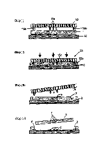
Fig. 1 is a side-view schematic diagram depicting an embodiment of the
patterning
process of the present invention for providing open-through holes in a TPE
membrane;
Fig. 2A depicts a scanning electron microscopy (SEM) side view cross-section
micrograph of a 90 pm thick TPE membrane with an array of 30 pm wide and 90 pm
tall
square-shaped open-through holes produced in the membrane by a process of the
present invention;
Fig. 2B depicts a scanning electron microscopy (SEM) top view micrograph of
one
of the open-through holes depicted in Fig. 2A;
14
CA 02829331 2013-08-14
WO 2012/109724
PCT/CA2011/000154
Fig. 3A depicts a scanning electron microscopy (SEM) side view cross-section
micrograph of a 90 pm thick TPE membrane with an array of 10 pm diameter and
90 pm
tall round open-through holes produced in the membrane by a process of the
present
invention;
Fig. 3B depicts a scanning electron microscopy (SEM) top view micrograph of
one
of the open-through holes depicted in Fig. 3A;
Fig. 4A and Fig. 4B depict SEM micrographs of an SU8 mold after two hot
embossing runs, where the mold has both thick protruding features used to
pattern open-
through holes and thin features to pattern channels;
Fig. 40 is a SEM micrograph depicting a bottom view of a TPE membrane with
open-through holes made by a patterning process of the present invention with
the mold
depicted in Figs. 4A and 4B;
Fig. 40 is a SEM micrograph depicting a top view of a TPE membrane with open-
through holes made by a patterning process of the present invention with the
mold
depicted in Figs. 4A and 4B;
Fig. 5A depicts a schematic diagram showing patterning of TPE without open-
through features;
Fig. 5B depicts a schematic diagram showing the patterning of TPE with open-
through features where stresses caused by shrinkage of TPE membrane during
cooling
causes defects;
Fig. 5C depicts a SEM micrograph showing an example of the defects that can
appear during cooling after patterning open-through TPE membranes;
Fig. 50 depicts a schematic diagram showing the patterning of TPE with open-
through features where a 100 pm thick elastic layer of PDMS is used to relieve
stresses
caused by shrinkage of TPE membrane during cooling;
Fig. 5E depicts a SEM micrograph showing an example of the an open-through
TPE membrane obtained from the process shown in Fig. 5D;
Fig. 6 is a schematic diagram depicting a process to fabricate and assemble
open-through membranes in 3D layered microfluidic spotting devices;
CA 02829331 2013-08-14
WO 2012/109724
PCT/CA2011/000154
Fig. 7 is a CAD schematic of one of the 3D layered microfluidic spotting
devices
fabricated by the process depicted in Fig. 6;
Fig. 8 depicts selected SEM micrographs illustrating the fabrication of the 3D
layered microfluidic spotting devices schematically depicted in Fig. 6 where:
(a) depicts
SU8 mold used for the fabrication of the bottom TPE membrane; (b) depicts a
top-side
view of the bottom TPE membrane; (c) depicts a bottom-side view of the bottom
TPE
membrane; (d) depicts the SUB mold used for the fabrication of the top TPE
membrane;
(e) depicts an overview of the top TPE membrane; and (f) depicts a close-up
view of the
top TPE membrane, in which scale bars in the insets of (a), (b), (c) and (d)
correspond
respectively to 50 pm, 2p pm, 10 pm and 200 pm. And the images shown in (d)
and (e)
were assembled from several SEM micrographs to achieve the desired field of
view;
Fig. 9 depicts photographs of the assembled 3D layered microfluidic spotting
device where (a) depicts the device before filling with dyes, (b) depicts the
device after
filling with red (R) and green dye (G), and (c) depicts a selected optical
microscope image
of the resulting red-green pattern obtained in the central region of the
device;
Fig. 10 depicts is a schematic drawing showing the mode of operation of a 3D
layered microfluidic spotting device of the present invention;
Fig. 11 depicts immobilization of Cy5-labeled DNA probes on a Zeonor substrate
with 3D layered microfluidic spotting devices of the present invention where
(a) depicts an
.. optical microscope image showing channels filled with the DNA solution,
(b)¨(c) depicts
fluorescence microscopic images of the immobilized DNA on the Zeonor
substrate, and
(d) depicts fluorescence intensity profile of the image shown in (c); and,
Fig. 12 depicts immobilization and hybridization of proteins on a Zeonor
substrate
with 3D layered microfluidic spotting devices of the present invention where
(a) depicts
.. optical microscope image showing channels filled with the rabbit IgG and
mouse IgG
solutions where the letters M and R shown in (a) indicate respectively the
position of
mouse IgG and rabbit IgG solutions, (b) depicts fluorescence microscopic image
of the
Zeonor substrate after hybridization with Cy5-labeled goat anti-rabbit IgG,
and (c) depicts
fluorescence microscopic image of the Zeonor substrate after subsequent
hybridization
with Cy3-labeled sheep anti-rabbit IgG where red (R) and green (G) colors in
(c) denote
respectively the Cy5 and Cy3 channels of the fluorescence microscope.
16
CA 02829331 2013-08-14
WO 2012/109724
PCT/CA2011/000154
Description of Preferred Embodiments
Materials and Methods:
Membranes and microfluidic devices described in the Examples were fabricated
either in VersaflexTM CL30 (from GLS corporation, McHenry, IL, USA), a melt-
processable elastomer based on styrene-ethylene/butylene-styrene block
copolymer, or
in EvataneTM 42-60 (from Arkema corporation, Colombes, France) a melt-
processable
elastomer based on ethylene-vinyl random copolymer. Throughout the Examples,
the
term TPE refers to either VersaflexTM CL30 or EvataneTM 42-60. VersaflexTM
CL30 and
Evatane TM 42-60 pellets as received were extruded at a temperature of 165 C
and 120 C,
.. respectively, to form films several meters long with thicknesses of about
90 pm, 140 pm
or 240 pm.
Molds were prepared by patterning one or two layers of spin-coated SU8
photoresist (3M1060 and GM1075; Gersteltec, Pully, Switzerland) on 100 mm
diameter
silicon wafers using standard photolithography processes (Geissler 2009b).
Photoplotted
films printed at a resolution of 65,000 dpi (Fineline Imaging, Colorado
Springs, CO, USA)
were used as the photolithography masks. After the patterning of the SU8
features, an
anti-adhesive treatment was applied on the molds by spin-coating a thin layer
of Teflon T"
AF (DuPont, Wilmington, DE, USA) and post-annealing at 200 C for 2h.
For the fabrication of the microfluidic devices, a piece of TPE was cut from
the
extruded film with scissors and placed between the mold and a counter-plate.
The
counter-plate comprised a silicon wafer coated with either 1H,1H,2H,2H-
perfluoro-
octyltrichlorosilane (Sigma-Aldrich, St. Louis, MO, USA) deposited from the
vapor phase
under reduced pressure, or a thin elastic layer of PDMS (SylgardTM 184, Dow
Corning
Corp., Midland, MI, USA) deposited by spin-coating a degassed prepolymer
solution and
curing at 200 C for 2h as a flexible layer. Hot-embossing was performed with
an EVG520
system (EV Group, Scharding, Austria) at a temperature of 170 C for
VersaflexTM CI30
and 110 C for Evatane TM 42-60, an applied force of 10 kN, and a ambient
pressure of 10-2
mbar. The oxygen plasma treatments (PlasmalabsT" 80plus, Oxford Instruments,
Bristol,
UK) were performed for 4 min at a pressure of 50 mTorr and 02 flow rate of 20
sccm.
Scanning electron microscopy (SEM) images were acquired with a Hitachi S-4800
(Hitachi High-Technologies Canada, Toronto, ON) and optical micrographs with a
Nikon
Eclipse L150 microscope (Nikon Instruments, Melville, NY). Microfabrication
steps and
device assembly were performed in class 1000 clean room facility.
17
CA 02829331 2013-08-14
WO 2012/109724
PCT/CA2011/000154
Numerical simulations were performed using a home-developed code based on
the Lattice-Boltzmann method with a two-phase three-dimensional D3Q19 scheme
driven
by a Shan¨Chen-type mesoscopic potential (Chen 1998; Clime 2009). The contact
angle
of the liquid with the surface of the spotting devices was set to a value of
about 56 by
adjusting the solid-liquid interaction potential. No external force was
applied on the liquid.
Protein and DNA immobilization assays were performed on Zeonor 1060R (Zeon
Chemicals, Louisville, KY) substrates fabricated by an injection molding
process. Before
the immobilization assays, the Zeonor slides were exposed to an ozone
treatment for
about 15 min using an Ozo 2vtt ozone generator (Ozomax, Shefford, QC, Canada).
They
were then incubated in a freshly prepared solution of 17 pM N-
hydroxysuccinimide (NHS;
Sigma-Aldrich) and 42 pM 1-ethyl-3-[3-dimethyl-aminopropyl]carbodiimide
hydrochloride
(EDC; Sigma-Aldrich) for 90 min, rinsed and blown dry with a stream of
nitrogen. As
received amino-modified 27-mer oligonucleotide solutions labeled with Cy3 or
Cy5
fluorophore (Integrated DNA Technologies, Coralville, IA) were first diluted
to 40 pM in
H20. This solution was then diluted 1:1 v/v with dimethyl sulfoxide (DMSO;
Sigma-
Aldrich) for the DNA immobilization assays. Mouse immunoglobulin G (IgG),
rabbit IgG,
Cy3-labeled sheep anti-mouse IgG, and Cy5-labeled goat anti-rabbit IgG were
purchased
from Jackson ImmunoResearch Laboratories (West Grove, PA) and were diluted to
their
final concentration in phosphate buffered saline (PBS, pH 7.4, Sigma-Aldrich).
For the immobilization assays, fabricated 3D layered TPE microfluidic spotting
devices were first placed on freshly activated Zeonor slides. The TPE
microfluidic devices
were found to conform spontaneously to most flat surfaces, thus providing a
reversible
watertight sealing to the Zeonor substrates without the need to apply
additional pressure
or heat. The immobilization solutions were placed on the selected inlets of
the fabricated
microfluidic devices using a pipette. After 2 h of incubation in humid
environment at room-
temperature, the Zeonor substrates were first immerged in a solution of 0.1%
sodium
dodecyl sulfate (SOS; Sigma-Aldrich) in PBS in which the microfluidic devices
were
peeled-off from the substrate. The Zeonor substrate was then washed in a new
bath of
0.1% SDS in PBS for 5 min and rinsed in water. The microfluidic devices were
used only
once to avoid cross-contamination issues. Before hybridization, the Zeonor
substrates
were blocked using a solution of 1 mg/ml bovine serum albumin (BSA; Sigma-
Aldrich) in
PBS for 15 min at room-temperature. For the hybridization, a 10 pl drop of the
target
solution was spread on top of the Zeonor substrate using a glass cover slip.
After
incubation times of respectively 5 min and 30 min for the protein and the DNA
assays, the
cover slip was removed and the Zeonor substrate was rinsed in PBS and water.
An
18
CA 02829331 2013-08-14
WO 2012/109724
PCT/CA2011/000154
Eclipse TE2000-U inverted fluorescence microscope (Nikon Instruments) equipped
with
an EM-CCD camera (Hamamatsu, Bridgewater, NJ) was used to characterize the
immobilized DNA and proteins labeled with Cy3 or Cy5 fluorophores.
Example 1: Fabrication of TPE membranes with micrometric open-through holes
Fig. 1 illustrates schematically a process of the present invention for the
fabrication of TPE membranes with open-through holes. As shown in Fig. 1 step
(i), pre-
extruded sheet 1 of TPE is first placed between mold 10 and flat counter plate
20. The
TPE sheet has a thickness that almost matches or exceeds slightly that of
highest
features 15a,15b of the mold. The highest features include features 15a for
producing
open-through holes in the membrane and features 15b for cutting the membrane
produced during hot embossing. As shown in Fig. 1 step (ii), assembly 30 is
then heated
to a temperature where the TPE is sufficiently softened and then pressed until
the highest
features of the mold nearly reach the counter plate, leaving only a submicron
thick excess
layer 8 of TPE between the highest features and the counter-plate. The
thickness of
excess layer 8 in Fig. 1 is exaggerated for clarity. As shown in Fig. 1 steps
(iii) and (iv),
on demolding, since this TPE excess layer 8 is thin enough, it detaches and
separates
systematically when formed TPE membrane 3 is removed from counter-plate 20,
thus
giving rise to open-through features 5 in membrane 3. Different surface
treatments
applied on the mold and counter-plate ensures that the open-through TPE
membranes
remain on the counter-plate during demolding (Fig. 1 step (iii)). The mold can
thus be
immediately used for another run and the counter-plate can then provide a hard
carrier to
facilitate the manipulation of the membranes in subsequent post-processing
steps. As
illustrated in Fig. 1, this technique also permits the cutting of the
membranes during the
patterning step by placing features 15b around each device on the mold. Using
a 100
mm diameter mold, it is possible to routinely pattern and precisely cut up to
32 TPE
membranes of 1x1 cm, each having multiple open-through holes, in a single step
process.
Fig. 2A shows a scanning electron microscopy (SEM) micrograph of an array of
pm wide and 90 pm tall square-shape open-through holes patterned in TPE by the
30 above process
using a mold fabricated with SU8 photoresist. The open-through holes
have a 3 to 1 aspect-ratio. Fig. 2B shows a top view of one of the open-
through holes.
The features of the membrane are well defined and no visible excess TPE layer
or
deformation is seen around the open-through holes.
19
CA 02829331 2013-08-14
WO 2012/109724
PCT/CA2011/000154
Fig. 3A shows a scanning electron microscopy (SEM) micrograph of an array of
pm diameter and 90 pm tall round open-through holes patterned in TPE by the
above
process using a mold fabricated with SUB photoresist. The open-through holes
have a 9
to 1 aspect-ratio. Fig. 3B shows a top view of one of the open-through holes.
The
5 features of the membrane are well defined and no visible excess TPE layer
or
deformation is seen around the open-through holes.
Fig. 4A and Fig. 4B show an SU-8 mold with 100 pm thick and 50 pm wide pillars
and 10 pm thick channels. The corresponding open-through TPE membrane after
two hot
embossing runs and demolding is shown in Fig. 4C and Fig. 4D. No damage is
seen on
10 the mold despite the significant undercut profile of the pillars,
therefore, this mold could
be reused for numerous hot embossing runs of open-through TPE membranes
despite
the significant undercut profile of the pillars.
By using a TPE sheet of the appropriate thickness as the starting material, it
is
possible to obtain open-through holes in less than 10 minutes embossing time
by
applying a relatively low force of 10 kN on the 100 mm diameter mold. Although
shorter
dwell time could be achieved at higher forces, this low force permits to use
repeatedly the
SU8 photoresist-based molds, thus eliminating the need for preparation of
costly metallic
molds. This demonstrates that a dense array of high aspect-ratio open-through
holes in
TPE membranes can be achieved with low-cost molds based on SU8 photoresist.
Example 2: Reducing appearance of defects in open-through TPE membranes during
fabrication
Although the present process provides considerable benefits to the ease of
patterning TPE, further improvement with respect to systematically improving
the quality
of the open-through TPE membranes would be beneficial. Stresses caused by the
relatively high shrinkage (1-2%) of the TPE membrane during the cooling step
can cause
the appearance of defects when open-through holes are punched in the
membranes.
This is in contrast to hot embossing of TPE where open-through holes are not
produced.
Fig. 5A depicts a schematic diagram showing the patterning of TPE without open-
through
features. Stresses produced by shrinkage of TPE membrane 40 during cooling are
.. relieved by vertical movement of counter-plate 41. In contrast, Fig. 5B
depicts a
schematic diagram showing the patterning of TPE with open-through features
where
counter-plate 45 cannot compensate for shrinkage of TPE membrane 44 during
cooling
and the stresses caused by this shrinkage leads to defects 46. Fig. 5C depicts
a SEM
CA 02829331 2013-08-14
WO 2012/109724
PCT/CA2011/000154
micrograph showing an example of the defects that can appear during cooling
after
patterning open-through TPE membranes.
As shown in Fig. 5D, to reduce the appearance of these defects, thin elastic
layer
57 of a thermoset rubber (e.g. a 100 pm thick layer of PDMS) can be placed
between
counter-plate 55 and TPE membrane 54, with the elastic layer in direct contact
with the
TPE membrane. The presence of this elastic layer helps to compensate for the
shrinkage
of the TPE membrane during cooling, which reduces the appearance of defects in
the
TPE membrane. Fig. 5E depicts a SEM micrograph showing an example of an open-
through TPE membrane obtained from the process shown in Fig. 5D. The membrane
shown in Fig. 5E does not have defects.
The process disclosed herein is significantly different than known processes
for
producing open-through holes in hard thermoplastic polymers (TP). As described
on
pages 152-161 of Worgull 2009, many techniques have been developed to pattern
open-
through holes in hard thermoplastics by hot embossing. For example, a polymer
layer and
.. a metal film, with the metal film in contact with the polymer being molded
can be placed
on the counter-plate plate. As Worgull indicates, by this technique it is
possible to keep
the residual layer in large contact surfaces, for example, at the margin
regions of the mold
insert, and to break the residual layer in small contact areas (e.g. the
features for making
open-through holes) so as to displace it completely into the layers placed on
the counter-
plate. These techniques thus rely on the permanent deformation of the layers
placed on
the counter-plate to break and remove the residual layer above each open-
through hole.
In the process disclosed herein, the adhesion of TPE to the counter-plate is
rather used
to directly break the residual layer during demolding without the need to
create
permanent deformation in layers placed on the counter-plate. This has several
advantages compared to previous art. First, in the previous art, one problem
arises from
the deformation of the flexible layer and the metal foil during the molding
process. The
mold inserts leave markers on the metal foil after successful molding of
through-holes,
which makes it impossible to use the metal foil twice. Also, the polymer layer
(e.g., PTFE
or PVDF) tends to deform under high load by flow processes. The second problem
is in
guaranteeing the demolding by adhesion of the residual layer on the substrate
plate.
Because of the missing adhesion of the typically thin residual layer on the
metal foil, the
replicated part has to be demolded manually, which can damage the structures.
The
process of the present invention suffers from neither of these two problems of
the prior
art.
21
CA 02829331 2013-08-14
WO 2012/109724
PCT/CA2011/000154
The use of an elastic layer on the counter plate is also significantly
different from
the previous art. As the elastic layer is made of a thermoset rubber and the
patterning
process does not result in the highest features of the mold actually punching
all the way
through the TPE into the elastic layer, the elastic layer is not deformed
permanently or
damaged during the process and can thus be reused for several runs. Also, the
permanent and irreversible plastic deformation that occurs in the layers used
in previous
art cannot provide the required uniform compressive force to the TPE layer, so
that
defects caused by TPE shrinkage could still be observed in the TPE membranes.
By
contrast, the elastic compression of the elastic layer can be released locally
(i.e. where
there is no open-through features) during cooling to compensate for shrinkage
of the
TPE.
Example 3: Fabrication and assembly of open-through TPE membranes in a 3D
layered
microfluidic device
A highly integrated 3D layered microfluidic spotter provides an example of a
3D
microfluidic device based on open-through TPE membranes. The 3D micrometric
patterning capability of the present process was used to produce a device that
can bring
liquid in contact only at some specific regions of a given substrate and that
integrates a
high density of inlet and outlets on a small footprint.
Fig. 6 is a schematic diagram summarizing an overall process for producing
several 3D layered microfluidic spotters in one process. In the process, first
open-
through TPE membrane 100 is produced to contain elements that function as
applicator
heads for the spotter. Fabrication steps for the first membrane are shown on
the left side
of Fig. 6 (Steps 1-5). Second open-through TPE membrane 200 is produced to
contain
elements that function as spotting holes for the spotter and is fabricated in
a similar
manner as the first membrane. Fabrication steps for the second membrane are
left out of
Fig. 6 for clarity. After producing the membranes, the first and second
membranes are
surface treated (if desired), aligned and assembled (Steps 6-9 in Fig. 6) to
form 3D
layered microfluidic spotters 300.
In more detail with reference to Fig. 6, to fabricate first open-through
membrane
100, a mold assembly is provided in Step 1. The mold assembly comprises mold
101,
counter-plate 107 and extruded TPE sheet 105 to be formed and patterned
between the
mold and counter-plate. The mold comprises SU8 photoresist and contains
features for
making open-through holes and features required to pattern several devices
simultaneously (e.g. wall features). The mold is covered with an anti-sticking
coating of
22
CA 02829331 2013-08-14
WO 2012/109724
PCT/CA2011/000154
Teflon T". The counter-plate comprises hard silicon wafer 102, flexible high
Tg heat
resistant Teflon T" sheet 103 and thin elastic PDMS layer 104. PDMS layer 104
is in
direct contact with TPE sheet 105. The TPE sheet is pre-extruded and has a
thickness
close to the highest features of the mold.
In Step 2 in Fig. 6, the TPE sheet is formed and patterned by heating the TPE
sheet to softening and applying pressure between the mold and counter-plate
until the
features of the mold for making open-through holes have almost punched through
the
TPE sheet (Step 3) leaving a thin excess layer of TPE between the features for
making
open-through holes and the thin PDMS layer of the counter-plate. In Step 4,
the TPE
sheet is demolded with the TPE sheet staying with the counter-plate. The low
adhesion
force between the TPE membrane and the anti-sticking coating on the mold
ensures that
the TPE membrane sticks on the PDMS layer. The mold can then be reused
immediately
for another run and the counter-plate is used to support the TPE membrane
during the
next steps.
In Step 5, extra TPE from open-through membrane 100 is peeled off from around
the parts of the membrane that will be formed into the spotters. In Step 6,
first and
second open-through TPE membranes 100,200 may be surface treated if desired,
for
example, to permanently change the surface from hydrophobic to hydrophilic. In
Step 7,
the hard silicon wafer of the counter-plate against which the second membrane
was
patterned is replaced with transparent hard plate 210 so that the first and
second
membranes can be properly aligned. In Step 8, the transparent plate is removed
and the
flexible sheet used in the production of the second membrane is peeled off the
aligned
membranes together with the thin PDMS layer. Further layers of the spotter can
be built
up, if desired, by repeating Steps 6-8 with one or more further open-through
membranes.
In Step 9, when all of the open-through membranes are aligned, they can be
bonded
permanently (for example by heating them for a few minutes) to form 3D
microfluidic
spotters 300. Contrary to hard thermoplastics, glass, and most other hard
materials, a
permanent thermal bond between TPE membranes can be obtained without applying
any
pressure. Further, for some TPE grades, the membranes will also create an
irreversible
and permanent bond when left in contact at room temperature for few hours. The
assembled 3D microfluidic spotters can then be stored and used individually at
a later
time. The process described in Fig. 6 can be performed in a highly parallel
fashion and
requires no manual manipulation of the TPE membranes to fabricate and assemble
the
3D microfluidic devices.
23
CA 02829331 2013-08-14
WO 2012/109724
PCT/CA2011/000154
Example 4: Design elements and operation of a 3D layered microfluidic spotter
Design elements:
As seen in Fig. 7, the 3D microfluidic spotters produced in Example 3 are
patterned with an array of 192 open-through holes, which are used as the
inlets and
outlets of the device. The spotter is based on two open-through TPE membranes.
The
top membrane defines the 96 inlets and 96 outlets while the bottom membrane is
patterned with both (i) a 10x10 array of 50 pm spotting holes located
centrally and (ii) 96
independent channels that connect the inlets, spotting holes, and outlets. The
spotter is
thus designed as a fluidic concentrator where the liquid dispensed in the
inlets is
transported by the channels and converge to the center of the spotter where
the actual
immobilization takes place on micron-size regions defined by the spotting
holes. The
dimensions of the spotters are kept to a low value of 1x1 cm in order to
increase the
number of spotters that can be patterned per run, but also to facilitate their
integration
with various detection systems where the area available to attach the spotter
is limited (as
for e.g. on microfabricated biosensor chips).
A rather high density of channels is required to address each of the spotting
holes
independently, which impose channel dimensions and inter-channel spacing in
the 5 to
10 pm range. Four of the 96 channels are connected to two spotting holes to
account for
the smaller number of inlets than spotting holes. To facilitate the manual
filling of the
spotters, the 96 inlets are kept as large as possible (500 pm diameter) and
are dispersed
evenly across the surface of the spotter, while the 96 outlets (150 pm
diameter) are
distributed across the edge of the spotter. The design of the spotters has
also been
optimized for the use of capillary action to drive the liquid in the channels.
It would be
unpractical to interface such a highly-integrated spotter with an external
pumping system.
The channels placed under the inlets are patterned in a "star-shape" to ensure
the correct
filling of the spotter by capillary action in the eventuality that the
dispensed liquid is not
distributed evenly in the inlet. The shape of the channels around the spotting
holes has
also been optimized to facilitate the filling of the holes by capillary
action.
In previous 3D microfluidic immobilization devices, isolated spots were
typically
obtained by transferring liquid back and forth from channels embedded inside
the device
to channels in contact with the substrate by using open-through holes (Chiu
2000;
Juncker 2002; Juncker 2005; Kloter 2004; Wang 2006). This geometry implies
that the
24
CA 02829331 2013-08-14
WO 2012/109724
PCT/CA2011/000154
area patterned on the substrate is larger than the open-through holes, as two
"vies" are
required to create each isolated spots. The immobilization of biological
probes on small
area thus critically depends on the fabrication of very small open-through
holes, which is
technically challenging. Also, in this layout, very high alignment accuracy is
required to
register properly the two layers of channels, which is particularly difficult
for elastomeric
materials (Chiu 2000). In the present spotter a single layer of channels is
used and the
biomolecules are immobilized directly by filling the open-through holes. With
this
geometry, the tolerance for the alignment between the top and bottom membranes
of the
device is relaxed to about 70 pm (while accuracy in the 5 to 10 pm range would
have
been required with the previous layout). Also, with this new design, spot size
of 50 pm
can be patterned without the need to punch open-through holes of smaller
dimensions.
The present design thus facilitates greatly the fabrication and assembly of
the spotters,
which is important when production at low-cost is being considered.
On the other hand, careful design of the channels around the spotting holes is
needed to reduce the possibility of trapping air bubbles above the spotting
holes during
assays. This is particularly challenging as the deep wells formed by the
spotting holes
naturally act as capillary valves that block the liquid front. To facilitate
the filling of the
spotters by capillary action, the layout of the channels was optimized with
the help of 3D
numerical simulations based on the Lattice-Boltzmann method (Chen 1998; Clime
2009).
Thus, the width of the channels leading to the spotting holes is increased
from 10 pm to
60 pm just before the 50 pm spotting hole is reached. The larger width of the
channel
permits the liquid to surround the spotting hole, which reduces the radius of
curvature of
the liquid front in the plane of the device. This, in turn, increases the
force exerted by the
capillary action, which helps filling the spotting holes. Both simulations and
experiments
indicate that it takes considerably longer to fill the spotting holes than the
surrounding
channels. Consequently, air bubbles are trapped if the liquid in the
surrounding channel
is not held in place until the hole is properly filled. The channel is thus
reduced abruptly
on the right hand side of the spotting hole to ensure that that the liquid
cannot reach the
exit channel before the hole is properly filled. Air bubbles can be trapped
when the width
of the channel is reduced gradually rather than abruptly after the spotting
hole. However,
for most practical purposes, air bubbles, although undesirable, were not
necessarily
highly problematic as they typically disappear after about 30 min incubation
time.
Fig. 8 shows SEM micrographs of a SU8/Si molds used for the fabrication of the
TPE membranes for the spotters. The mold for the bottom membrane comprises two
SU8 layers, one being an 8 pm thick layer to define the channels and the other
being a
CA 02829331 2013-08-14
WO 2012/109724
PCT/CA2011/000154
100 pm thick layer patterned in a 10x10 array of pillars to create the open-
through holes.
Figs. 8(b) and 8(c) show images from the corresponding bottom TPE membrane
after
patterning. Fig. 8(b) shows the top side of the bottom TPE membrane where both
the
channels (that will be embedded inside the final spotters) and the top of the
spotting holes
are seen. In Fig. 8(c), the bottom TPE membrane has been flipped to reveal the
openings that will be in contact with the substrate during immobilization
assays. Both the
channels and spotting holes are seen to be replicated very accurately. Even
the
submicron roughness of the SU8 molds is accurately reproduced in the TPE layer
(not
shown). The elastomeric nature of the TPE facilitates demolding and prevents
the
formation of defects resulting from undercut features, sidewall roughness, or
shrinkage
(which are commonly observed for the hot embossing of hard thermoplastics
(Worgull
2009)).
Fig. 8(d) shows one of the 32 regions of the SU8 mold (200 pm thick, 100 mm
diameter) used to pattern the top TPE membranes of the spotters. In addition
to the
pillars used to punch the inlets and outlets, the SU8 wall surrounding each of
the
individual regions is also visible. The SEM micrographs of Fig. 8(e) and 8(f)
show the
corresponding open-through TPE membranes. These images highlight how the
present
invention can be used not only to pattern microscopic vies and spotting holes,
but also to
punch in a highly parallel manner the large number of inlets and outlets
required in the
proposed design and to effortlessly cut each of the individual membranes with
very high
accuracy.
After the patterning by hot embossing, the bottom and top TPE membranes were
exposed to 02 plasma to render their surface hydrophilic. This treatment was
performed
while the membranes were still attached to the hard counter-plate, thus
allowing
numerous membranes to be treated simultaneously with a minimum of
manipulation.
Alignment of the top and bottom membranes was achieved by placing an x-y-z
manipulator on top of the x-y-z-theta stage of an optical microscope. The top
membrane
was placed facing down on a transparent sheet of Teflon TM attached to the x-y-
z
manipulator, while the bottom membrane was placed on a substrate that was
deposited
on the microscope stage. When acceptable alignment was achieved, the x-y-z
manipulator was lowered until the two membranes were touching. Due to the
rather weak
attachment force between TPE and Teflon TM, the top membrane could be easily
transferred and attached to the bottom membrane. No other bonding steps were
necessary to operate the spotters due to the reversible watertight sealing
capability of
TPE.
26
CA 02829331 2013-08-14
WO 2012/109724 PCT/CA2011/000154
General Operation:
Fig. 9 shows an assembled spotter attached to a transparent plastic substrate.
Despite the relatively small dimensions and high inlet density of the
spotters, a trained
user can fill reliably the inlets by hand using a pipette. For example, Fig.
9(b) shows a
spotter where every inlet is filled with either a red dye R or green dye G.
The dyes have
been positioned in the inlets so as to from the red-green chessboard pattern
seen in Fig.
9(c), thus demonstrating the possibility of individually addressing the
spotting holes.
Since the liquid tends to align itself on the cavities formed by the inlets,
the dispensed
droplets can be placed quite accurately on the surface of the devices despite
the
positional error introduced by hand pipetting (see Fig. 3(b)).
Fig. 10 depicts a schematic drawing showing the general mode of operation of
the
spotter. In operation, substrate 400 to be spotted is surface activated as
depicted in Step
1 to form activated region 401. Spotter 410 is applied on the substrate in
Step 2. In Step
3, the reagents to be spotted are introduced in liquid form into inlets 411
and the liquid is
.. drawn through channels 412 by capillary action to exit through outlets 413
whereupon
spots 420 of the reagents are formed on substrate 400.
Example 5: Use as a 3D layered micro fluidic spotter for immobilization of
biological
probes
Fig. 11 shows an example of a typical DNA immobilization assay in which the 3D
microfluidic spotting devices of the present invention have been used to
pattern amino-
modified Cy5-labeled DNA probes on an activated Zeonor plastic substrate. As
seen in
Fig. 11(a), some of the channels of the spotter have been filled selectively
with the DNA
solution so as to pattern the letters "IMI" while the other channels were left
empty. Fig.
11(b) shows a fluorescence image of the Zeonor substrate after immobilization,
removal
of the spotter, and washing. The 50 pm Cy5-labeled DNA spots corresponding to
the
channels filled during the assay are clearly seen. The edges of the spots are
sharply
defined and their relative positioning is controlled very accurately. As seen
in Fig. 11(c)
and 11(d), the uniformity of each spot is also excellent with an rms variation
in
fluorescence intensity of only 2%. This result contrasts with the uniformity
typically
obtained by techniques such as pin spotting, where it is challenging to
achieve high spot
uniformity at this scale. On the other hand, as visible on Fig. 11(b), spot-to-
spot
variations of the fluorescence intensity on the order of 20% rms were observed
even if the
same analyte was used to pattern each spot. This variation may arise from the
partial
27
CA 2829331 2017-07-07
evaporation of the liquid deposited in the inlets during the filling of the
spotters and from the
difficulties in controlling precisely the volume dispensed in each inlet.
An immobilization and hybridization assay performed with proteins is also
shown on
Fig. 12. For this assay, solutions of unlabeled mouse IgG and rabbit IgG (5
mg/m1) were
dispensed to selected inlets of the devices according to the layout shown in
Fig. 12(a) for
the immobilization on an activated Zeonor substrate. As the biological probes
were
unlabeled in this assay, the Zeonor substrate showed no significant
fluorescent signal after
immobilization of the IgG proteins. The substrate was then sequentially
exposed to Cy5-
labeled goat anti-rabbit IgG (10 .pg/m1) and Cy3-labeled sheep anti- mouse IgG
(10 pg/m1).
Fig. 12(b) shows the fluorescence signal recorded after hybridization with
only the Cy5-
labeled goat anti-rabbit IgG. As expected, a strong Cy5 fluorescence signal is
measured
only on the spots patterned with rabbit IgG. Relatively high hybridization
selectivity was
obtained; the measured Cy5 fluorescence intensity was about 150 times lower on
the
mouse IgG spots than on the rabbit IgG spot. Fig. 12(c) shows a Cy3 (green, G)
and Cy5
(red, R) combined fluorescence image obtained after subsequent hybridization
of the
Zeonor substrate with Cy3-labeled sheep anti- mouse IgG. Hybridization of the
anti-mouse
IgG was also found to be highly selective with significant Cy3 fluorescent
signal detected
only on the mouse IgG spots. These results confirm the integrity of the
immobilized protein
array and show that the 3D microfluidic devices we propose can be used to
immobilize high
quality protein and DNA arrays.
References:
Abgrall P, Lattes C, Condra VR, Dollat X, Colin SP, Gu AM. (2006) A novel
fabrication
method of flexible and monolithic 3D microfluidic structures using lamination
of SU-8 films.
=
Journal of Micromechanics and Microengineering. 16, 113.
Anderson JR, Chiu DT, Jackman RJ, Cherniayskaya 0, McDonald JC, Wu H,
Whitesides
SH, Whitesides GM. (2000) Fabrication of Topologically Complex Three-
Dimensional
Microfluidic Systems in PDMS by Rapid Prototyping. Anal. Chem. 72(14), 3158.
Anderson JR, Chiu DT, Jackman RJ, Cherniayskaya 0, McDonald JO, Whitesides GM.
(2008) Microfluidic systems including three-dimensionally arrayed channel
networks. United
States Patent Publication US 2008/0122140 published May 29, 2008.
Bartholomeusz DA, Boutte RW, Andrade JD. (2005) Xurography: Rapid Prototyping
of
Microstructures Using a Cutting Plotter. J. Microelectromech, Syst. 14(6),
1364.
28
CA 02829331 2013-08-14
WO 2012/109724
PCT/CA2011/000154
Bartolo D, Degre G, Nghe P, Studer V. (2008) Microfluidic stickers. Lab Chip.
8, 274.
Bodas D, Khan-Malek C. (2006) Formation of more stable hydrophilic surfaces of
PDMS
by plasma and chemical treatments. Microelectron. Eng. 83, 1277.
Bruzewicz DA, Boncheva-Bettex M, Whitesides GM, Siegel A, Weibel DB,
Shevkoplyas
S, Martinez A. (2007) Fabrication of Conductive Pathways, Microcircuits and
Microstructures in Microfluidic Networks. International Patent Publication WO
2007/061448 published May 31, 2007.
Carvalho BL. (2004) Elastomeric Tools for the Fabrication of Elastomeric
Devices and
Uses Thereof. United States Patent Publication US 2004/0241049 published
December
2,2004.
Chang-Yen DA, Myszka DG, Gale BK. (2006) J. Microelectromech. Syst. 15, 1145-
1151.
Chen S, Doolen GD. (1998) Annu. Rev. Fluid. Mech. 30, 329-364.
Chen C-S, Breslauer DN, Luna JI, Grimes A, Chin W-C, Leeb LP, Khine M. (2008)
Shrinky-Dink microfluidics: 3D polystyrene chips. Lab Chip. 8, 622.
Chen IJ, Lindner E. (2007) The Stability of Radio-Frequency Plasma-Treated
Polydimethylsiloxane Surfaces. Langmuir. 23(6), 3118.
Chiu DT, Jeon NL, Huang S, Kane RS, Wargo CJ, Chai IS, Ingber DE, Whitesides
GM.
(2000) Patterned deposition of cells and proteins onto surfaces by using three-
dimensional microfluidic systems. Proc. Natl. Acad. Sci. U.S.A., 97(6) 2408-
2413.
Chiu DT, Pezzoli E, Wu H, Stroock AD, Whitesides GM. (2001) Using three-
dimensional
microfluidic networks for solving computationally hard problems. Proceedings
of the
National Academy of Sciences. 98(6), 2961.
Chow CYH. (2001a) Multi-layer microfluidic devices. United States Patent US
6,167,910
issued January 2, 2001.
Chow CYH. (2001b) Multi-layer microfluidic devices. United States Patent US
6,321,791
issued November 27, 2001.
Chow CYH). (2002) Multi-layer microfluidic devices. United States Patent US
6,494,230
issued December 17, 2002.
29
CA 02829331 2013-08-14
WO 2012/109724 PCT/CA2011/000154
Clime L, Brassard D, Veres T. (2009) Microfluid. Nanofluid. DOI:
10.1007/s10404-10009-
10491-10409.
Corcoran CS, Jaecklein WJ, Pricone RM, Thielman WS, Chiu CC-W, Chen DH-P.
(2004)
Sheet Having Microsized Architecture. United States Patent Publication US
2004/0126538 published July 1, 2004.
Corcoran CS, Jaecklein WJ, Pricone RM, Thielman WS, Chiu CC-W, Chen DH-P.
(2005)
Sheet Having Microsized Architecture. United States Patent Publication US
2005/0118393 published June 2,2005.
Duffy DC, Jackman RJ, Vaeth KM, Jensen KF, Whitesides GM. (1999)
Electraluminescent Materials with Feature Sizes as Small as 5 pm Using
Elastomeric
Membranes as Masks for Dry Lift-Off. Adv. Mater. 11(7), 546.
Eddings MA, Miles AR, Eckman JW, Kim J, Rich RL, Gale BK, Myszka DG. (2008)
Anal.
Biochem. 382, 55-59.
Eddings MA, Eckman JW, Arana CA, Papalia GA, Connolly JE, Gale BK, Myszka DG.
(2009) Anal. Biochem. 385, 309-313.
Geissler M, Roy E, Deneault J-S, Arbour M, Diaz-Quijada GA, Nantel A, Veres T.
(2009a)
Stretching the Stamp: A Flexible Approach to the Fabrication of Miniaturized
DNA Arrays.
Small. 5(22), 2514-2518.
Geissler M, Roy E, Diaz-Quijada GA, Galas J-C, Veres T. (2009b) ACS App!.
Mater.
Interfaces. 1, 1387-1395.
Griscom L, Degenaar P, LePioufle B, Tamiya E, Fujita H. (2001) Jpn. J. App!.
Phys. 40,
5485-5490.
Haraldsson KT, Hutchison JB, Sebra RP, Good BT, Anseth KS, Bowman CN. (2006)
3D
polymeric microfluidic device fabrication via contact liquid photolithographic
polymerization (CLiPP). Sensors and actuators. B, Chemical. 113, 454.
Heckele M, Durand A. (2001) Microstructured through-holes in plastic films by
hot
embossing. Proceedings of 2nd international conference of the European society
for
precision engineering and nanotechnology. p.196.
Heckele M, Guber AE, Truckennnuller R. (2006) Replication and bonding
techniques for
integrated microfluidic systems. Microsystem Technology. 12, 1031.
CA 02829331 2013-08-14
WO 2012/109724
PCT/CA2011/000154
Heo YS, Cabrera LM, Song JW, Futai N, Tung Y-C, Smith GD, Takayama S. (2007)
Characterization and Resolution of Evaporation-Mediated Osmolality Shifts That
Constrain Microfluidic Cell Culture in Poly(dimethylsiloxane) Devices. Anal.
Chem. 79(3),
1126.
Hofmann 0, Voirin G, Niedermann P, Manz A. (2002) Anal. Chem. 74, 5243-5250.
Hutchison JO, Haraldsson KT, Good BT, Sebra RP, Luo N, Ansetha KS, Bowman CN.
(2004) Robust polymer microfluidic device fabrication via contact liquid
photolithographic
polymerization (CLiPP). Lab Chip. 4, 658.
Jeon NL, Chiu DT, Wargo CJ, Wu H, Chai IS, Anderson JR, Whitesides GM. (2002)
Design and Fabrication of Integrated Passive Valves and Pumps for Flexible
Polymer
3-Dimensional Microfluidic Systems. Biomed. Microdevices. 4(2), 117.
Jeon NL, Chiu DT, Wargo CJ, Choi IS, Wu H, Anderson JR, Whitesides GM,
McDonald
JC, Metallo SJ, Stone HA. (2004) Valves and pumps for microfluidic systems and
method
for making microfluidic systems. United States Patent Publication US
2004/0228734
published November 18, 2004,
Jo B-H, Lerberghe LMV, Motsegood KM, Beebe DJ. (2000) Three-Dimensional Micro-
Channel Fabrication in Polydimethylsiloxane (PDMS) Elastomer. J.
Microelectromech.
Syst. 9(1), 76.
Juncker D, Schmid H, Drechsler U, Wolf H, Wolf M, Michel B, de Rooij N,
Delamarche E.
(2002) Anal. Chem. 74, 6139-6144.
Juncker D, Schmid H, Delamarche E. (2005) Nat. Mater. 4, 622-628.
Karp CD, Pezzuto M, Maresch L, O'Connor SD. (2002) Microfluidic valve with
partially
restrained element. United States Patent Publication US 2002/0155010 published
October 24, 2002.
Kartalov EP, Walker C, Taylor CR, Anderson WF, Scherer A. (2006) Microfluidic
vies
enable nested bioarrays and autoregulatory devices in Newtonian fluids. PNAS.
103(33),
12280.
Kikutani Y, Horiuchi T, Uchiyama K, Hisarnoto H, Tokeshi M, Kitamori T. (2002)
Glass
microchip with three-dimensional micro channel network for 2 x 2 parallel
synthesis. Lab
chip. 2, 188.
31
CA 02829331 2013-08-14
WO 2012/109724
PCT/CA2011/000154
Kim JY, Lee JYBKA, Lee SH. (2005) Automatic aligning and bonding systelll of
PDMS
layer for the fabrication of 3D microfluidic channels. Sens. Actuators, A.
119, 593.
Kloter U, Schmid H, Wolf H, Michel B, Juncker D. (2004) Technical Digest of
the 17th
IEEE International Conference on Micro Electro Mechanical Systems. pp. 745-
748.
Lee JN, Park C, Whitesides GM. (2003) Solvent Compatibility of
Poly(dimethylsiloxane)-
Based Microfluidic Devices. Anal. Chem. 75(23), 6544.
Lee J, Ismagilov RF, Jiang X, Kenis PJA, Ferrigno R, Whitesides GM. (2004)
Fluidic
arrays and method of using. United States Patent Publication 2004/0258571
published
December 23, 2004.
Liu RH, Stremler MA, Sharp KV, Olsen MG, Santiago JG, Adrian RJ, Aref H, Beebe
DJ.
(2000) Passive mixing in a three-dimensional serpentine microchannel. J.
Microelectromech. Syst. 9(2), 190.
Luo Y, Zare RN. (2008) Perforated membrane method for fabricating three-
dimensional
polydimethylsiloxane microfluidic devices. Lab Chip. 8, 1688.
Maltezos G, Garcia E, Hamahan G, Gomez FA, Vyawhare S, van Dam RE, Chena Y,
Scherer A. (2007) Design and fabrication of chemically robust three-
dimensional
microfluidic valves. Lab Chip. 7, 1209.
Martin DWM, Bennett WD. (1999) Microfabrication methods for microchannel
reactors
and separations systems. Chem. Eng. Commun. 173, 245.
Martin PM, Matson DW, Bennett WD, Stewart DC. (2000) Laminated Ceramic
Microfluidic
Components for Microreactor Applications. Proceedings of the 4th International
Conference on Microreaction Technology. vol. 1998.
Martinez AW, Phillips ST, Whitesides GM. (2008) Three-dimensional microfluidic
devices
fabricated in layered paper and tape. PNAS. 105(50), 19606.
Mazzeo AD, Dirckx M, Hardt BE. (2007) Single-step through-hole punching by hot
embossing. Annual technical conference - Antec, Conference proceedings. 5,
2931.
Mehne C, Steger R, Koltay P, Warkentin D, Heckele MP. (2008) Large-area
polymer
microstructure replications through the hot embossing process using modular
molding
tools. Proc. IMechE Vol. 222 Part B: J. Engineering Manufacture. 93-99.
32
CA 02829331 2013-08-14
WO 2012/109724
PCT/CA2011/000154
Mukhopadhyay R. (2007) When PDMS isn't the best. Anal. Chem. 79(9), 3248.
Natarajan G, Humenik JN. (2006) 3D Ceramic Microfluidic Device Manufacturing.
Journal
of Physics: Conference Series. 34, 533.
Natarajan P, Yao D, Ellis TS, Azadegan R. (2007) Through-thickness embossing
process
for fabrication of three-dimensional thermoplastic parts. Polym. Eng. Sci. 47,
2075.
Natarajan S, Hatch A, Myszka DG, Gale BK. (2008a) Anal. Chem. 80, 8561-8567.
Natarajan S, Katsamba PS, Miles A, Eckman J, Papalia GA, Rich RL, Gale BK,
Myszka
DG. (2008b) Anal. Biochem. 373, 141-146.
O'Connor SD, Pezzuto M, Dantsker E. (2002) Multi-layer microfluidic device
fabrication.
United States Patent Publication US 2002/0112961 published August 22, 2002.
O'Connor SD, Karp CD, Dantsker E. (2003a) Microfluidic flow control devices.
United
States Patent Publication US 2003/0196695 published October 23, 2003.
O'Connor SD, Karp CD. (2003b) Microfluidic regulating device. United States
Patent US
6,619,311 issued September 16, 2003.
Peng Z-C, Ling Z-G, Tondra M, Liu C-G, Zhang M, Lian K, Goettert J, Hormes J.
(2006)
CMOS Compatible Integration of Three-Dimensional Microfluidic Systems Based on
Low-
Temperature Transfer of SU-8 Films. J. Microelectromech. Syst. 15(3), 708.
Romanato F, Tormen M, Businaro L, Vaccari L, Stomeo T, Passaseo A, Fabrizio
ED.
(2004) X-ray lithography for 3D microfluidic applications. Microelectron. Eng.
73-74, 870.
Ryu W, Fasching RJ, Vyakarnam M, Greco RS, Prinz FB. (2006) Microfabrication
Technology of Biodegradable Polymers for Interconnecting Microstructures. J.
Microelectromech, Syst. 15(6), 1457.
Schift H, Bellin S, Gobrecht J. (2006) Perforated polymer membranes fabricated
by
nanoinnprint. Microelectron. Eng. 83(4-9), 873.
Sodunke TR, Turner KK, Caldwell SA, McBride KW, Reginato MJ, Moses Noh H.
(2007)
Micropatterns of Matrigel for three-dimensional epithelial cultures.
Biomaterials. 28, 4006.
33
CA 02829331 2013-08-14
WO 2012/109724
PCT/CA2011/000154
Stoyanov I, Koch MTSGM, Uihndorf M. (2005) Low-cost and chemical resistant
microfluidic devices based on thermoplastic elastomers for a novel biosensor
system.
Mater. Res. Soc. Symp. Proc. 872, 169.
Stoyanov I, Tewes M, Koch M, Lohndorf M. (2006) Microfluidic devices with
integrated
active valves based on thermoplastic elastomers. Microelectron. Eng. 83, 1681.
Sudarsan AP, Ugaz VM. (2004a) Printed Circuit Technology for Fabrication of
Plastic-
Based Microfluidic Devices. Anal. Chem. 76, 3229.
Sudarsan AP, Wang J, Ugaz VM. (2004b) Novel thermoplastic elastomers for
microfluidic
device construction. 8th International Conference on Miniaturized Systems for
Chemistry
and Life Sciences. p. 22.
Sudarsan AP, Wang J, Ugaz VM. (2005) Thermoplastic Elastomer Gels: An Advanced
Substrate for Microfluidic Chemical Analysis Systems. Anal. Chem. 77(16),
5167.
Therriault D, White SR, Lewis JA. (2003) Chaotic mixing in three-dimensional
microvascular networks fabricated by direct-write assembly. Proteins: Struct.,
Funct.
Bioinf. 2,265.
Toepke MW, Beebe DJ. (2006) PDMS absorption of small molecules and
consequences
in microfluidic applications. Lab Chip. 6, 1484.
Trimbach D, Feldman K, Spencer ND, Broer DJ, Bastiaansen CWM. (2003) Block
Copolymer Thermoplastic Elastomers for Microcontact Printing. Langmuir.
19(26), 10957-
10961.
Veninga EP, Koetse MM. (2008) Device built by joining a plurality of layers.
European
Patent Publication EP 1 935 843 published June 25, 2008.
Vickers JA, Caulum MM, Henry CS. (2006) Generation of Hydrophilic
Poly(dimethylsiloxane) for High-Performance Microchip Electrophoresis. Anal.
Chem.
78(21), 7446.
Vozzi G, Flaim C, Ahluwalia A, Bhatia S. (2003) Fabrication of PLGA scaffolds
using soft
lithography and microsyringe deposition. Biomaterials. 24, 2533.
Wang Z-H, Meng Y-H, Ying P-Q, Qi C, Jin G. (2006) Electrophoresis. 27, 4078-
4085.
34
CA 02829331 2013-08-14
WO 2012/109724
PCT/CA2011/000154
Weigl BH, Bardell R, Schulte T, Battrell F, Hayenga J. (2001) Design and Rapid
Prototyping of Thin-Film Laminate-Based Microfluidic Devices. Biomed.
Microdevices. 4,
267.
Wen W, Shang P, Niu X, Liu L. (2008) Constructing planar and three-dimensional
microstructures with pdms-based conducting composite. International Patent
Publication
WO 2008/0123174 published May 29, 2008.
Whitesides GM, Anderson JR, Chiu DT, Jeon N-L, Huang S, Kane R, Choi IS,
Ingber DE.
(2004) Patterning of surfaces utilizing microfluidic stamps including three-
dimensionally
arrayed channel networks. United States Patent Publication US 2004/0121066
published
June 24,2004.
Whitesides GM, Phillips ST, Martinez AW, Butte MJ, Wang A, Thomas S, Sindi H.
(2008)
Patterned Paper as a Platform for Inexpensive, Low Volume, Portable Bioassays
and
Methods of Making Same. International Patent Publication WO/2008/049083
published
April 24, 2008.
Worgull M. 2009. Hot Embossing ¨ Theory and Technology of Microreplication.
(William
Andrew publisher, O)cford, UK) Section 5.5.3.2, pages 154-157.
Wu H, Odom TVV, Chiu DT, Whitesides GM. (2003) Fabrication of Complex Three-
Dimensional Microchannel Systems in PDMS. Journal of the American Chemical
Society.
125(2), 554 (2003).
Yoon L-B, Han C-H, Yoon E, Kim C-K. (1988) Novel monolithic and multilevel
integration
of high-precision 3-D microfluidic components. Proceedings of SPlE The
International
Society for Optical Engineering. 3515, 183.
Zhao S, Cong H, Pan T. (2009) Direct projection on dry-film photoresist (DP2):
Do-it-
yourself three-dimensional polymer microfluidics. Lab Chip. 9, 1128-1132.
Other advantages that are inherent to the structure are obvious to one skilled
in
the art. The embodiments are described herein illustratively and are not meant
to limit
the scope of the invention as claimed. Variations of the foregoing embodiments
will be
evident to a person of ordinary skill and are intended by the inventor to be
encompassed
by the following claims.
35