Note: Descriptions are shown in the official language in which they were submitted.
CA 02832863 2013-10-09
WO 2012/150509 PCT/1B2012/051219
1
ELECTRO-THERMAL ANTIFOG OPTICAL DEVICES
Background
A continuing problem attendant with the use of optical glasses, goggles,
face shields, and other optical devices in both medical and industrial
applications is
fogging of the viewing substrate. The warm, moist air exhaled by the wearer
will
condense on relatively cool surfaces that are in close proximity to the nose
or
mouth of the user. Condensate droplets will fog the viewing surfaces, which
may
seriously impair vision.
Various approaches have been attempted to alleviate the problems due to
fogging on goggles and glasses. For example, passive coatings for surfaces
have
been described that function by absorbing moisture and/or spreading the
moisture
across a surface to eliminate droplet formation that leads to fogging.
Examples of
passive coatings have been described in U.S. Patent Nos. 4,767,671 and
5,668,618. More recently, active approaches have been suggested for use in
preventing condensate that leads to misting or fogging of a surface. For
example,
U.S. Patent No. 6,470,696 describes a device including two thermal sensors,
one
in contact with a surface and the other in contact with a cooling device. The
device
also includes a humidity sensor. A circuit causes a condensation removal
mechanism to be activated for removing liquid from the surface when the
humidity
sensor indicates the presence of condensation based upon the readings of the
thermal sensors. In another example, German publication DE 3323670 describes
a visor that includes a strip of conductive material attached to the visor and
terminals for electrical connection to a current source to heat the visor via
the strip
and prevent misting of the visor.
While the above describe improvement in the art, room for additional
improvement exists. What are needed in the art are active coatings for
prevention
of condensation, for example, fog, on surfaces.
Summary
According to one embodiment, disclosed is an optical device including a
transparent lens, a conductive transparent layer on a surface of the
transparent
lens, and a power supply. The conductive transparent layer includes a
crosslinked
network including a polythiophene, thiophene functionalized carbon based
CA 02832863 2013-10-09
WO 2012/150509 PCT/1B2012/051219
2
nanostructures, and a transition metal crosslinking agent. In addition, the
power
source is in electrical communication with the conductive transparent layer.
Also disclosed is a substrate defining a first surface and comprising a
conductive transparent layer on the first surface, the conductive transparent
layer
comprising a crosslinked network including poly(3,4-ethylene-dioxythiophene)
(PEDOT), polystyrene sulfonic acid (PSS), thiophene derivatized carbon
nanotubes, and a transition metal crosslinking agent.
Brief Description of the Drawings
A full and enabling disclosure of the subject matter, including the best mode
thereof, directed to one of ordinary skill in the art, is set forth more
particularly in
the remainder of the specification, which makes reference to the appended
figures
in which:
Fig. 1 is a schematic illustration of a pair of goggles including a coating as
described herein.
Fig. 2 graphically illustrates the temperature increase of a polycarbonate
surface by use of a coating composition as described herein.
Detailed Description of Representative Embodiments
Reference now will be made in detail to various embodiments of the
disclosed subject matter, one or more examples of which are set forth below.
Each example is provided by way of explanation, not limitation. In fact, it
will be
apparent to those skilled in the art that various modifications and variations
may be
made in the present disclosure without departing from the scope or spirit of
the
subject matter. For instance, features illustrated or described as part of one
embodiment may be used on another embodiment to yield a still further
embodiment. Thus, it is intended that the present disclosure covers such
modifications and variations as come within the scope of the appended claims
and
their equivalents.
The present invention is directed to optical devices including an active layer
on a surface for the prevention of fogging of the surface. The layer is formed
from
a composition that includes a conductive polymer and functionalized carbon
based
nanostructures. The functionalized carbon based nanostructures may improve the
electrical characteristics of the layer beyond what is capable of the
conductive
polymer alone. To provide further improvement, the composition includes a
CA 02832863 2013-10-09
WO 2012/150509 PCT/1B2012/051219
3
transition metal crosslinking agent that may form a complex with both the
conductive polymer and the functionalized carbon based nanostructures. The
layer formed of the composition is crosslinked with the transition metal
compound.
Accordingly, the crosslinked matrix includes the conductive polymer, the
carbon
based nanostructures, and the transition metal crosslinking agent, all of
which may
be in electrical communication with one another. As the carbon based
nanostructures are connplexed within the crosslinked network, and not merely
blended with the polymer of the layer, improved electrical contact may be
obtained.
This may provide a layer with excellent electrical characteristics at low add-
on
levels of the carbon based nanostructures. In one embodiment, scratch
resistant
hard coat solution materials may be combined with the other components of the
composition to improve the mar and abrasion resistance of the layer without
adversely affecting the electrical characteristics of the layer.
The crosslinked layer may be placed in electrical communication with a
power source to complete a circuit. Current flow through the circuit may lead
to an
increase in the temperature of the surface, which may prevent fogging of the
surface. Hence, a transparent substrate including the layer on a surface may
be
beneficially utilized in optical devices such as goggles, optical glasses,
safety
glasses, welding lenses (both fixed and variable shades), visors, face
shields, and
so forth.
As utilized herein, the term 'fogging' refers to condensate on a surface such
that visualization through the surface is impaired, as in a transparent lens,
or such
that the ability to visualize the surface itself is impaired. The condensate
droplets
cause the scattering of incident light and decrease in visualization, or
fogging.
The composition includes one or more conductive polymers suitable for use
in forming a translucent or transparent layer. As utilized herein, the term
'translucent' refers to a material having a transmission of light in the
visible
spectrum (between about between about 300 nanometers and about 800
nanometers) of between about 30% and about 85%. As utilized herein, the term
'transparent' refers to material having a light transmission in the visible
spectrum
greater than about 85%. In one embodiment, a transparent film may have a light
transmission of greater than about 90%, or greater than about 95%. A coated
substrate may have a percent haze of less than about 5%, or less than about
3%.
CA 02832863 2013-10-09
WO 2012/150509 PCT/1B2012/051219
4
Haze is defined as the percentage of transmitted light, which, in passing
through
the specimen, deviates from the incident beam by more than an average of 25
degrees. Haze is commonly referred to as the "milkiness" of a specimen, or its
loss in contrast. Translucency, transparency, and haze may be measured by a
comparison of the intensity of the incident light to that of the light passing
through
the material according to standard protocols. For instance, by use of testing
methods described in ASTM D1003 ¨ 07e1 entitled "Haze and Luminous
Transmittance of Transparent Plastics," (D01: 10.1520/D1003-07).
In general, the composition used to form the conductive layer may be
aqueous, though small amounts of solvents may be present in the composition,
as
is known. For instance, small amounts of solvents, for instance less than
about
5% by weight of the composition, may be included such as alcohols, benzene,
pyrrolidone, fornwl amines, glycol ethers, and so forth. The composition may
contain, for instance, at least about 75 wt.% water, in some embodiments at
least
about 90 wt.% water, and in some embodiments, at least about 96 wt.% water.
The conductive, transparent polymer of the coating composition may be a
polythiophene, which encompasses polythiophene as well as any derivative
thereof. In general, a coating composition can include less than about 3% by
weight of a polythiophene, or less than about 1 /0 by weight in another
embodiment.
For instance, the composition can include between about 0.01% by weight and
about 1% by weight of a polythiophene. A polythiophene may have a structure
of:
is
R10 OR2
wherein R1 and R2 are independently selected from hydrogen, or a 01-04 alkyl
group or R1 and R2 together form an optionally substituted 01-04 alkylene
radical,
for instance a methylene radical that is optionally substituted with alkyl
groups, a
1,2-ethylene radical that is optionally substituted with 01-012 -alkyl or
phenyl
groups, or a 1,2-cyclohexylene radical.
In one preferred embodiment, the composition may include the
polythiophene derivative poly(3,4-ethylenedioxythiophene) having the
structure:
CA 02832863 2013-10-09
WO 2012/150509 PCT/1B2012/051219
o/ \0 \
0 0
0 0 0 0 0 0
\
Any suitable method may be utilized for forming a polythiophene. For
example, poly(3,4-ethylenedioxythiophene) may be formed via the oxidation of a
3,4-ethylenedioxythiophene monomer leading to withdrawal of an electron from
the
5 3,4-ethylenedioxythiophene heteroaromatic ring. Oxidants may include,
without
limitation, iron (III) salts, such as FeCI3, Fe(CI04) and the iron (III) salts
of organic
acids and of inorganic acids containing organic radicals. Other suitable
oxidants
may include H202, K2Cr207, alkali metal persulphates, ammonium persulphates,
alkali metal perborates and potassium permanganate. The combination of two
oxidized monomers will form a dimer with release of a proton. Further
oxidation of
dimers will lead to formation of trimers, etc., until long poly(3,4-
ethylenedioxythiophene) chains are formed. The ionization potential of 3,4-
ethylenedioxythiophene monomers and poly(3,4-ethylenedioxythiophene) dimers,
trimers, and infinitely long chains are 1.1, 0.46, 0.16 and -0.25V (vs.
Ag/Ag+),
respectively. Consequently, once oligomers are formed, polymerization may
accelerate rapidly.
It should be understood that the compositions are not limited to poly(3,4-
ethylenedioxythiophene), and other polythiophenes as well as blends of two or
more polythiophenes are encompassed herein including, without limitation,
poly(3-
methylthiophene), poly(3-ethylthiophene), poly(3-propylthiophene), poly(3-
butylthiophene), poly(3-hexylthiophene), poly(3-heptylthiophene), poly(3-
octylthiophene), poly(3-decylthiophene), poly(3-dodecylthiophene), poly(3-
octadecylthiophene), poly(3-bromothiophene), poly(3-chlorothiophene), poly(3-
iodothiophene), poly(3-cyanothiophene), poly(3-phenylthiophene), poly(3,4-
dimethylthiophene), poly(3,4-dibutylthiophene), poly(3-hydroxythiophene),
poly(3-
methoxythiophene), poly(3-ethoxythiophene), poly(3-butoxythiophene), poly(3-
hexyloxythiophene), poly(3-heptyloxythiophene), poly(3-octyloxythiophene),
poly(3-decyloxythiophene), poly(3-dodecyloxythiophene), poly(3-
CA 02832863 2013-10-09
WO 2012/150509 PCT/1B2012/051219
6
octadecyloxythiophene), poly(3,4-dihydroxythiophene), poly(3,4-
dimethoxythiophene), poly(3,4-diethoxythiophene), poly(3,4-
dipropoxythiophene),
poly(3,4-dibutoxythiophene), poly(3,4-dihexyloxythiophene), poly(3,4-
diheptyloxythiophene), poly(3,4-dioctyloxythiophene), poly(3,4-
didecyloxythiophene), poly(3,4-didodecyloxythiophene), poly(3,4-
propylenedioxythiophene), poly(3,4-butenedioxythiophene), poly(3-methy1-4-
methoxythiophene), poly(3-methyl-4-ethoxythiophene), poly(3-carboxythiophene),
poly(3-methyl-4-carboxythiophene), poly(3-methyl-4-carboxyethylthiophene), and
poly(3-methyl-4-carboxybutylthiophene).
As polythiophenes tend to be insoluble, the composition may include a
secondary component that may improve the solubility of the polymer. For
example,
a composition may include poly(3,4-ethylenedioxythiophene) in conjunction with
the water soluble cationic polyelectrolyte polystyrene sulfonic acid having
the
structure:
1110
SO3H SO3H SO3H
Poly(3,4-ethylenedioxythiophene)/ polystyrene sulfonic acid compositions
may be formed according to known methodology (for example, using the
polyelectrolyte polystyrene sulfonic acid as the charge-balancing dopant
during the
poly(3,4-ethylenedioxythiophene) polymerization process), or alternatively may
be
obtained commercially. For example, prepared PSS/PEDOT mixture may be
purchased from Aldrich or other companies with a solids content of about 1.3-
2.6%.
In such a case, the solution may be adjusted as needed or may alternately be
directly used in formulation. Poly(3,4-ethylenedioxythiophene)/
polyelectrolyte
polystyrene sulfonic acid available under the Clevios TM brand is also
available from
Heraeus of Hanau, Germany. In general, the ratio of poly(3,4-
ethylenedioxythiophene) to polyelectrolyte polystyrene sulfonic acid may be
between about 1 and about 2.5 by weight, though this is not a requirement of a
composition, and any suitable ratio of the two is encompassed herein.
CA 02832863 2013-10-09
WO 2012/150509 PCT/1B2012/051219
7
Any other method for solubilizing a polythiophene may be utilized in forming
a composition. For instance, in one embodiment poly(3,4-
ethylenedioxythiophene)-tetramethyl acrylate may be utilized. poly(3,4-
ethylenedioxythiophene)- tetramethyl acrylate is an ABA block copolymer that
includes branched end-capping tetrannethyl acrylate groups that promote
dispersibility.
The total amount of polymer in a composition, for instance the total amount
of polythiophene and polymeric solubilizer can be between about 1.5% and about
3% by weight of the composition.
In addition to the conducting polymer and any stabilizer, the composition
includes carbon based nanostructures. An amount of conductive and/or
semiconductive carbon based nanostructures may be included in the formed
matrix so as to enhance the electrical characteristics of the layer formed
from the
composition without sacrificing the transparency of the coating.
The carbon based nanostructures may include any structure that has at
least one dimension on a nanometer scale. In particular, while the
nanostructures
may, in certain embodiments, describe very high aspect ratios, for instance
greater
than 1000 nanometers, and may include a length dimension that is on a larger
scale, they will define at least one dimension on a nanometer scale, for
example,
In one embodiment, the carbon based nanostructures may be carbon
nanotubes or carbon nanospheres (for example, buckyballs, nanoonions, or other
fullerenes). Carbon nanotubes may be single-walled carbon nanotubes, multi-
CA 02832863 2013-10-09
WO 2012/150509 PCT/1B2012/051219
8
about 200 nanometers, while an individual single-walled carbon nanotube may
have an outer diameter of less than about 5 nanometers. In general, individual
multi-walled carbon nanotubes may have an outer diameter between about 5
nanometers and about 100 nanometers.
The carbon based nanostructures may be formed according to any known
method or procedure. For instance, carbon nanotubes may be formed according
to an electric arc method, a laser-vaporization method, a HiPco method, a
chemical vapor deposition method, or any other method as is known in the art.
Carbon nanotubes may be formed according to any known methodology or may be
obtained on the commercial market. For example, multi-walled carbon nanotubes,
single-walled carbon nanotubes, or double walled nanotubes are available from
NanoLab, Inc. of Waltham, Massachusetts; Nano-C, Inc. of Westwood,
Massachusetts; or Unidym of Sunnyvale, California.
Depending upon the formation technique, the carbon-based nanostructures
may be mixed with an amount of impurities such as soot, catalysts, nucleators,
and
so forth upon formation. The carbon based nanostructures may be purified
following formation and prior to addition to the coating composition. For
instance,
the carbon based nanostructures may be provided to the composition at greater
than about 90% purity.
In one embodiment, an as-formed carbon based nanostructure composition
may be purified by subjection to heating in an oxidizing atmosphere, treatment
with
a strong acid, often while being subjected to sonication, followed by a final
wash.
However, it should be understood that any purification process as is known in
the
art may optionally be utilized.
The carbon based nanostructures may be functionalized to facilitate
distribution of the nanostructures throughout the composition as well as to
facilitate
crosslinking of the polymeric matrix during formation of the coating layer.
More
specifically, the carbon based nanostructures may be functionalized with a
thiophene derivative to encourage distribution of the nanostructures
throughout the
polythiophene-based coating composition.
The preferred thiophene derivative for coupling with the carbon based
nanostructures may vary, depending upon the functionalization scheme to be
utilized. For instance, in one embodiment, the carbon based nanostructures may
CA 02832863 2013-10-09
WO 2012/150509 PCT/1B2012/051219
9
be activated through oxidation of the structures to introduce carboxylic acid
groups
on the structures, and an amine derivative of thiophene may be coupled to the
nanostructures through formation of an amide bond. In one preferred
embodiment,
the carbon based nanostructures may be functionalized through coupling with 2-
aminothiophene via amide bond formation.
Other coupling reactions may alternatively be utilized, primarily depending
upon the initial activation groups of the nanostructures and the corresponding
thiophene derivative. For instance, carbon nanotubes may be activated through
reaction of the carbon nanotubes with fluorine gas to provide fluorine
derivatized
nanotubes and then further derivatized via nucleophilic substitution with a
desired
nucleophile, for example, an alkyl lithium species, substituted hydrazines, or
alkyl
amines. The activated carbon nanostructures may then be reacted with an
appropriate derivative of thiophene according to known chemistries to form the
thiophene functionalized nanostructures.
The composition may include an amount of thiophene functionalized carbon
based nanostructures so as to enhance conductivity of a layer formed of the
composition without sacrificing the transparency of the layer. For example, a
coating composition may include less than about 5% by weight of the carbon
based nanostructures, less than about 3% by weight or less than about 1% by
weight.
The thiophene functionalized carbon based nanostructures may be readily
dispersed throughout an aqueous poly(3,4-ethylenedioxythiophene) solution. In
one embodiment, dispersion may be enhanced by sonication that can be applied
for a period of time of between about 5 minutes up to several hours. The
various
components may be combined in different ways, and the method of forming the
composition is not critical. For instance, the thiophene functionalized
nanostructures may be combined with a formed poly(3,4-ethylenedioxythiophene)/
polyelectrolyte polystyrene sulfonic acid dispersion, or alternatively, the
thiophene
functionalized nanostructures may first be combined with a polyelectrolyte
polystyrene sulfonic acid solution via, for example, mixing in conjunction
with
sonication, and this solution may then be combined with a poly(3,4-
ethylenedioxythiophene) dispersion.
CA 02832863 2013-10-09
WO 2012/150509 PCT/1B2012/051219
The composition also includes a crosslinking agent that may crosslink the
polymer/nanostructure matrix following application to a surface. The
crosslinking
agents may include transition metal ions and/or transition metal salts. While
not
wishing to be bound to any particular theory, it is believed that a transition
metal
5 crosslinking agent will complex with the sulfur atom of the thiophene
groups of
both the poly(3,4-ethylenedioxythiophene) and the functionalized carbon based
nanostructures, forming a coating including a conductive crosslinked matrix
including both polymeric components and the nanostructures.
Transition metals encompassed herein include any element in the d-block of
10 the periodic table, i.e., any element in groups 3 through 12 of the
periodic table. In
another embodiment, transition metals encompassed herein include those
elements having an incomplete d sub-shell, which would encompass any element
in groups 3 through 11 of the periodic table. In one embodiment, transition
metals
for use as a crosslinking agent may include manganese, iron, cobalt, nickel,
copper, silver, gold, platinum, palladium, vanadium and chromium. For example,
the transition metal may be iron, copper, silver, gold, cobalt or nickel. In
general,
the transition metal crosslinking agent may be a transition metal ion or a
transition
metal salt of the formula MX,, wherein M is a transition metal, X is a halogen
negative ion, sulfur atom or a conjugate base negative ion of an acid, and n
is an
integral number of 1 to 6. Examples of suitable crosslinking agents include,
without limitation, halide, chloride, sulfate, acetate, ammonium, or nitrate
salts of
transition metals such as ferric chloride, ferric sulfate, ferric nitrate,
cupric chloride,
as well as combinations of transition metal compounds.
The transition metal crosslinking agent may be dissolved or dispersed into
the composition. In the case of a transition metal powder dispersed in the
composition, a particle size of the metal powder may be below about 10
micrometers (p.m). If desired, a surface of the metal powder may be oxidized
with
a diluted weak acid such as acetic acid. The composition may include the
transition metal crosslinking agent in a concentration of between about 0.1
wt. %
and about 2.0 wt. A of the coating composition. For instance, the metal ion
concentration in the composition can be between about 0.1M and about .001M.
The composition may include additional constituents, as desired. For
example, in those embodiments in which the composition will form an antifog
CA 02832863 2013-10-09
WO 2012/150509 PCT/1B2012/051219
11
coating on a visualization surface such as a pair of goggles, the composition
may
include one or more additional materials that may impart scratch and/or
chemical
resistance, anti-reflective characteristics, and so forth. For instance, a
coating
composition may include an amount of a hydroxylated fluoropolymer or a
siloxane
based resin and a crosslinking agent therefore as is known in the art, which
may
provide scratch and weather resistance to the coating. For example, the
composition may include between about 5 wt.% and about 20 wt.% of a scratch
resistant hard coat resin such as a siloxane polymer resin, an acrylic polymer
resin,
or a hydroxylated polymer comprising fluorine-containing monomer units such as
tetrafluoroethylene or chlorotrifluoroethylene, and optionally including
fluorine-free,
ethylenically unsaturated monomer units. A fluoropolymer may include more than
about 20% by weight of fluorine. The composition may also include a
crosslinking
agent for the hydroxylated fluoropolymer such as, for example, methylamine
and/or polysilicic acid.
The composition may also include one or more binders that may improve
the adhesion of the crosslinked matrix to a substrate. Examples of useful
binders
include, without limitation, polyvinyl acetate, polycarbonate, polyvinyl
butyrate,
polyacrylates, polymethacrylates, polystyrene, polysulfonated styrene,
polyacrylonitrile, polyvinyl chloride, poly-butadiene, poly-isoprene,
polyethers,
polyesters, silicones, pyrrole/acrylate, vinyl acetate/acrylate,
ethylene/vinyl acetate
copolymers, polyvinyl alcohols, and any derivatives or mixtures thereof.
Binders
may be included in a composition in relatively small amounts, for instance
less
than about 10% by weight of the composition.
Following formation, the composition may be coated onto a substrate. The
composition may be used immediately upon formation, or alternatively may be
stored for a period of time, for instance for several days, prior to use. A
layer
formed by the composition may completely cover a surface of a substrate or may
partially cover a surface. For instance, a layer may be applied to a surface
in a
pattern. A pattern will be a continuous pattern, such that a current can flow
through the formed layer, but need not completely cover a substrate surface.
The substrate may be organic or inorganic, flexible or rigid, and of any
suitable size and shape. For instance, a substrate may be polymeric or
ceramic.
In one preferred embodiment, the substrate may be a transparent material for
use
CA 02832863 2013-10-09
WO 2012/150509 PCT/1B2012/051219
12
in an optical application such as lenses for glasses, goggles or other
oculars, face
shields or visors for helmets or face masks, and so forth. In one embodiment,
a
substrate may be a glass, for instance an optical-grade glass such as a
borosilicate glass or a fluorite glass. In another embodiment, a substrate may
be a
polymeric material for use in an optical application including thermoplastic
materials such as polycarbonates, polyesters such as polyethylene
terephthalate
or polybutylene terephthalate, polystyrenes, polysulfones, polyethersulfones,
cellulose acetate butyrate and thermoplastic polyurethanes; or thermoset
materials
such as diethyleneglycol bis allylcarbonate polymers and copolymers, thermoset
polyurethanes, polythiourethanes, polyepoxides, polyepisulfides, polyacrylates
including poly(meth)acrylates such as polymethylmethacrylate,
polythio(meth)acrylates, as well as copolymers and blends thereof.
A substrate may be in the form of a single or multilayered film, sheet, panel
or pane of material, and may be formed by any well-known process, such as
blowing, casting, extrusion, injection molding, and so forth. In one
embodiment,
the composition may be coated between two layers of a multilayer substrate.
For
instance, a layer may be formed between glass or polymer substrates.
The composition may be coated onto one or more surfaces of the substrate
according to any suitable coating method or combinations of methods including,
without limitation, dip coating, spin coating, spray coating, printing (for
example,
rotogravure), bar coating, solution coating, blade coating, slot-die coating,
and so
forth. In one embodiment, the composition may be coated on a single surface of
a
substrate, for example, an inner surface of a face shield. In other
embodiments,
however, the composition may be coated on both an inner and outer surface of a
substrate or may envelope an entire substrate.
To ensure uniform coating and/or wetting of the substrate, the substrate
may be oxidized prior to coating using, for example, corona discharge, ozone,
plasma, or flame treatment methods. In some embodiments, a substrate may also
be applied with a pretreatment to facilitate uniform application of the
coating
composition thereto. For instance, a primer such as polyvinylidene chloride or
polyvinyl chloride may be applied to a transparent substrate. Typically, the
primer
does not have a substantial affect on the optical properties of the
transparent
substrate.
CA 02832863 2013-10-09
WO 2012/150509 PCT/1B2012/051219
13
The average thickness of the resulting coating can be less than about 5
microns in thickness, or less than about 2 microns, in one embodiment. For
example, the average thickness of the layer can be between about 0.8 and about
1.2 microns.
According to one embodiment, the average thickness of the resulting
coating may be selected to minimize glare. Specifically, a single-layer
optical
coating having a thickness equal to the wavelength of incident light will
result in
reflections from the air-coating boundary and coating-substrate boundary that
are
1800 out of phase with each other, thereby causing destructive interference
and
reducing total reflectance. Thus, in those embodiments in which the wavelength
of
incident light may range from about 200 nanometers to about 1000 nanometers,
the average thickness of the coating may range from about 50 nanometers to
about 250 nanometers. In addition, because 550 nanometers is the wavelength at
which the human eye displays a peak photo-optic response, the average coating
thickness may be about 140 nanometers in one embodiment. It should be
understood, however, that the coating is not limited to a single layer, but
may also
contain multiple layers. For example, it is readily understood by those
skilled in the
art that two layers may be utilized, with each layer being optimized in
thickness to
minimize reflection of different wavelengths of light, thus providing anti-
glare
properties over a wide spectrum of light. In addition, while the average
coating
thickness may be uniform, the actual coating thickness may vary considerably
from
one particular point on the coating to another. Such variations in thickness,
when
correlated over a visibly distinct region, may be beneficial by contributing
to
broadband anti-reflective properties of the coating.
The coating may be dried and cured in air and optionally with the addition of
energy to increase the cure rate. For example, the coated substrate may be
cured
in an oven at a temperature of from about 20 C to about 150 C, in some
embodiments from about 50 C to about 130 C, and in some embodiments, from
about 100 C to about 120 C. Alternative cure methods as are known may be
utilized, such as by subjecting the coated surface to irradiation, for
example,
microwave irradiation. Once dried and cured, the conductive polymer component
of the layer may constitute at least about 50 wt.%, in some embodiments at
least
CA 02832863 2013-10-09
WO 2012/150509 PCT/1B2012/051219
14
about 75 wt.%, and in some embodiments, at least about 90 wt.% of the cured
layer.
The sheet resistance (Rs) of a layer is a function of the bulk resistivity of
the
layer and the layer thickness. It is a measure of electrical resistance in a
thin film
that is nominally uniform in thickness and capable of approximation as a two
dimensional system. Sheet resistance may be described in units of ohms or
optionally as ohms per square (Ohms/sq.), where "square" is dimensionless.
Ohms per square is exclusively utilized when describing sheet resistance, and
thus
may be used to differentiate the two dimensional resistance from a three
dimensional system. Sheet resistance may be measured using a four-point probe,
in which a direct current is applied between two outer current electrodes and
a
voltage is measured between two inner electrodes located within the two outer
electrodes, with the current flowing along the plane of the film. Four-point
probes
utilize a geometric correction factor based on the orientation and spacing of
the
electrodes in the probe to correct the voltage/current ratio measured by the
probe.
The resistivity of the film may be calculated from the sheet resistance by
multiplying the sheet resistance by the thickness of the film. In one
embodiment, a
cured film formed of the conductive polymer composition may have a sheet
resistance of between about 300 Ohms/square and about 900 Ohms/square, for
instance between about 330 Ohms/square and about 890 Ohms/square. In
another embodiment, the sheet resistance may be less than about 300
Ohms/square, less than about 175 Ohms/square, less than about 150
Ohms/square, or less than about 100 Ohms/square.
The conductivity (a) of a coating is the measure of the electrical conduction
of the material. Conductivity may be measured by applying a differential
electric
field across the layer and monitoring the electrical current that results. The
conductivity is then calculated by dividing the current density by the
strength of the
applied electric field. Conductivity is the reciprocal of electrical
resistivity, thus
conductivity may be calculated from sheet resistance by taking the reciprocal
of
the sheet resistance multiplied by the film thickness (a=1/(Rs x t). A film as
described herein may have a conductivity of greater than about 100 siemens per
centimeter, greater than about 450 siemens per centimeter, greater than about
600
siemens per centimeter, or greater than about 750 siemens per centimeter. In
one
CA 02832863 2013-10-09
WO 2012/150509 PCT/1B2012/051219
preferred embodiment, a film may have a conductivity greater than about 400
siemens per centimeter, for instance between about 185 and about 485 siemens
per centimeter, in one embodiment.
Optionally, additional layers may be formed on the substrate, either beneath
5 the conductive layer, above the conductive layer, or at a different
location on the
substrate as the conductive layer. For instance, an anti-reflective coating
and/or a
scratch resistant coating may be formed on top of the conductive layer or may
be
formed on the opposite side of a substrate.
In one embodiment, a scratch resistant coating may be formed on top of the
10 conductive layer. Alternatively, the components of the conductive layer
and the
scratch resistant coating can be combined together to form a single coating
composition. For instance, following cure of the conductive layer and any
necessary connection formation for electrical communication to a power source
(for example, electrode formation), a scratch resistant and/or chemical
resistant
15 coating may be formed on the conductive layer. A scratch resistant
coating may
include a crosslinked hydroxylated fluoropolymer formed in a separate layer,
or
any other scratch resistant coating as is known in the art.
In one embodiment, a siloxane-based hard coat may be formed on the
substrate. For example, a siloxane-based coating may be prepared by adding
polymerizable components such as tetraalkyl orthosilicate, epoxyalkylalkoxy
silanes, and (meth)acryloxyalkylalkoxy silanes in a solvent mixture containing
an
acid catalyst and other additives as are known in the art. The polymerizable
components can generally be included in the solvent mixture in an amount of
between about 15% and about 55% by weight. For instance, the polymerizable
mixture may contain between about 40% and about 60% by weight of tetraalkyl
orthosilicates, between about 15% and about 45% by weight of epoxyalkylalkoxy
silanes and between about 5% and about 15% by weight of
(meth)acryloxyalkylalkoxy silanes. The total solvent mixture may contain
between
about 20% and about 60% by weight water, between about 10% and about 25%
by weight of a solvent mixture, between about 0.05 % and about 0.5% by weight
of
2M HCI and between about 0.4% and about 2.5% by weight of acetic acid together
with between about 0.1% and about 1.2% by weight of wetting agents and
CA 02832863 2013-10-09
WO 2012/150509 PCT/1B2012/051219
16
between about 0.1% and about 0.5% by weight of other catalysts or curing
agents
as are known in the art.
Examples of tetraalkyl orthosilicate include but are not limited to
tetramethyl
orthosilicate, tetraethyl orthosilicate, tetrapropyl orthhosilicate, and
tetrabutyl
orthosilicate.
Examples of epoxysilanes used in the invention include but are not limited
to 1-glycidoxyethyltrimethoxysilane, 2-glycidoxypropyltriethoxysilane, 3-
glycidoxypropyltrimethoxysilane, 3-glycidoxypropyltriethoxysilane, 3-
glycidoxybutyltrimethoxysilane, and other derivatives with different
substitutions.
Examples of methacryloxy silanes include but are not limited to 2-
methacryloxypropyltrimethoxysilane, 2-methacryloxypropyltriethoxysilane, 2-
methacryloxypropylmethyldimethoxysilane, 3-acryloxypropyltrimethoxysilane, 3-
acryloxypropyltriethoxysilane and other derivatives.
An anti-reflective coating may be included on a substrate, either on the
same surface as the conductive layer or on a different surface, as desired. An
anti-reflective coating acts to reduce the reflection at the surface, allowing
a higher
level of visible light transmission. Typically, anti-reflective coatings
include several
different sub-layers comprising many different materials such as, but not
limited to,
aluminum oxide, zirconium oxide, magnesium flouride, silicon dioxide,
cryolite,
lithium fluoride, thorium tetrafluoride, cerium fluoride, lead fluoride, zinc
sulfide,
zinc scandium sulfide, silicon, tellerium, magnesium oxide, yttrium oxide,
scandium
oxide, silicon oxide, hafnium oxide, zirconium dioxide, cerium oxide, niobium
oxide,
tantalum oxide, and titanium oxide.
The thickness of each sublayer is often related to an even whole number
division of the wavelength of light that is most preferred to be transmitted
through
the coated material. Typical sublayer thicknesses required to achieve a
particular
visible light transmission level are also known in the art.
In one embodiment, an anti-reflecting coating may be applied by vacuum
deposition according to one of the following techniques: by evaporation,
optionally
ion beam-assisted; by spraying using an ion beam; by cathode sputtering; or by
plasma-assisted vapor-phase chemical deposition.
Following formation, the conductive layer may be placed in electrical
communication with a power source that may apply a voltage across the film and
CA 02832863 2013-10-09
WO 2012/150509 PCT/1B2012/051219
17
instigate a current flow. The current flow may heat the film and the
surrounding
area, causing a temperature increase at the surface and thereby preventing
water
vapor condensation as droplets on the surface.
In one preferred embodiment, a coated transparent substrate may be a
component of a pair of goggles. In this regard, one embodiment of a pair of
goggles that may contain the coated transparent substrate will now be
described in
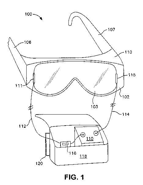
more detail. Referring to Fig. 1, a pair of goggles 100 is shown including a
frame
102 and a transparent lens 103. Side bows 106, 107 are attached to the
opposite
sides of the frame 102 for securing the goggles during use. Though illustrated
as
side bows, the goggles may alternatively incorporate straps, bands, or any
other
device for securing the goggles 100 to the wearer's head. The frame 102 may
include a shaped portion 110 on the top and bottom (not shown) that may fit
snugly
against the forehead and face of a wearer to further protect the eyes of the
wearer.
The lens 103 may be formed of a transparent substrate, such as a glass or
a polycarbonate and may extend across the majority of the wearer's field of
vision.
In another embodiment, a pair of goggles may be formed with two separate
lenses
that may function only for protective purposes or may also be corrective
lenses.
The cured film is formed on a surface of the lens 103 and placed in
electrical communication with a power supply 110, such as a battery. Any
battery
as is known in the art can be utilized including either rechargeable batteries
or
disposable batteries. For instance, a lithium ion battery 110 may be in
electrical
communication with a first electrode 111 by means of a first lead 112, for
example
a cathode lead at 7.5 volts. The first electrode 111 may also be in electrical
communication with the conductive layer. In addition, a second lead 114, for
example, an anode lead, may be in electrical communication with a second
electrode 115 that is on the opposite side of the lens 103. The battery 110
may be
a component of a power pack 118. The power pack 118 may also include a switch
116 that may be in electrical communication with the other electrical
components
of the system. The power pack may include one or more loops 120 that may be
used to connect the power pack to a convenient location such as the wearer's
belt,
jacket, or so forth. The loops 120 may be replaced with any suitable
connecting
device such as hooks, clips, bands, etc.
CA 02832863 2013-10-09
WO 2012/150509 PCT/1B2012/051219
18
In one embodiment, the battery may be within or on the goggles. For
example, a battery may be attachable to the frame of the goggles, for instance
in a
battery casing that is accessible for battery replacement. In this embodiment,
a
switch may also be included on the frame for completion of a circuit.
Upon closing the switch 116, a circuit may be completed that passes
through the conductive layer of the goggles 100. Current flow through the
coating
layer may increase the temperature of the layer by an amount that is
sufficient to
prevent condensation forming on the lens 103 while not being uncomfortably
warm
for a wearer. For instance, upon completion of the circuit, the temperature of
the
surface of lens 103 may increase by less than about 5 C, or less than about 4
C in
another embodiment. In one embodiment, the temperature of the surface of the
lens 103 may increase between about 2 C and about 5 C.
In another embodiment, an active conductive layer may be formed on a
facemask. For example, a facemask may include a visor attached to a filter
body.
The coating may be formed on the visor and placed in electrical communication
with a power source, such as a power pack illustrated in Fig. 1. The visor is
formed from a transparent substrate and is dimensioned to fit across the width
of
the filter body and extend over the eyes of the wearer. In one particular
embodiment, the visor may be formed from polyethylene terephthalate. A
facemask also includes a filter body attached to the visor. The filter body is
designed to retard the flow of liquids to the nose and mouth of the wearer.
The
filter body may be formed in any manner known to those skilled in the art. As
will
be appreciated by those skilled in the art, the filter body may be constructed
from
any of a variety of different materials and contain any number of desired
layers.
Although various configurations have been described above, it should be
understood that the present disclosure is not limited to any particular
substrate.
For example, in one embodiment, a transparent conductive film may be formed on
an optical device such as goggles, glasses, facemasks, etc., and in another
embodiment, a transparent conductive film may be formed on a substrate for a
different application, for instance in forming a window, a viewscreen, and so
forth.
The present disclosure may be further understood with reference to the
Examples provided below.
CA 02832863 2013-10-09
WO 2012/150509
PCT/1B2012/051219
19
Example 1
1) Semiconductive solution preparation:
PSS/PEDOT semiconductive solution was prepared by mixing PSS and
PEDOT solids (raw materials are commercially available from Aldrich) with
deionized
water in an amount of 1.5-3.0 % by weight of the solution at 55 C for 6
hours.
Following, the suspension was sonicated for 3 hours to insure a homogeneous
mixture. During the reaction, the pH value (pH = 1-4) was adjusted by use of
2M
H2SO4.
2) Meta110-solvent preparation:
Metal salts such as Ni(NO3)2, CuSO4, and AgNO3 were dissolved in deionized
water individually to effect a metal ion concentration range from 10-1-10-3 M.
The
prepared metal solutions were added to 0.5% wt of DMSO to prevent electro-
chemical
reduction.
3) Carbon nanotube precursor solution:
Oxidation of Carbon Nanotubes: 0.5-2.5 wt % of single wall carbon nanotubes
were first sonicated in mixed nitric acid/sulfuric acid (1/4 ratio in volume)
for 4 hours.
Upon cooling, the solution was diluted with D. I. Water. The oxidized CNT were
collected by filtration and washed with water until the filtrate measured pH =
7. The
black CNT were dispersed again in water and sonicated with mixed H2SO4 and
H202
for 4 hours; the final product was filtered and washed with water, then dried
under
vacuum at room temperature.
Thiothene functionalized CNT: Under N2 atmosphere, 5-10 wt % of oxidized
CNT (compared to the amount of 2-aminothiophene) were stirred at room
temperature
with 10-20 wt % of DCC (dicyclohexylcarbodiimide) and dry DMF for 8 hours, and
then
the sealed flask was sonicated for 1 hour at room temperature. 2-
aminothiophene was
dissolved in dry DMF and added to above solution at room temperature, the
mixture
was then agitated for 4 hours at 80 C with inert N2. The product was
collected
through filtration and washed with methanol, acetone, DMF, and water,
respectively,
and dried under vacuum for 8 hours at 60 C.
0.5-3.0 wt % of the thiophene functionalized carbon nanotubes were sonicated
for 30 minutes with DMF/H20, and then the solution was stirred at 90 C for 8
hours
until a homogeneous solution was formed.
CA 02832863 2013-10-09
WO 2012/150509
PCT/1B2012/051219
The solution was used for blending quickly. If stored for 24 hours or more, a
precipitate may form, requiring the solution to be sonicated again for 30 min
before
incorporating it into a formulation.
4) Synthesis of semiconductive coating solution:
5 In a round bottom flask, 95-99 wt. A. of the PSS/PEDOT solution
(prepared in
step 1) was added to 1-5 wt. % of the CNT solution (prepared in step 3), and
then the
mixture was sonicated for 1 hour and stirred at room temperature for 4 more
hours.
The solution was used immediately.
The PSS/PEDOT/CNT solution was added drop-wise to 1-10 wt. % of a
10 solution of metal ions (prepared in step 2) under constant agitation at
room
temperature and stirred for 3 hours to ensure complete blending. Then, the
solution
was sonicated for 1.5 hours.
5) Preparation of Siloxane Hard Coat:
A coating solution was prepared by mixing 208 g of tetraethyl orthosilicate,
90 g
15 of glycidoxypropyltrimethoxy silane, 10 g of
methacryloxypropyltrimethoxy silane, 238
g of isopropyl alcohol, 46 g of water, 0.8 g of 2M HCI and 6.4 g of 2M acetic
acid in a
flask. The solution was mixed at room temperature to partially hydrolyze the
silanes
and to achieve a clear solution. The solution was then heated at 70 C for 1-2
hours
while stirring to completely hydrolyze the silanes. Following, the solution
was cooled to
20 room temperature followed by addition of 3.2 g of surfactant (BrijR98,
available from
Sigma-Aldrich, Inc.), and 2.4 g of aluminum acetylacetonate. The solution was
stirred
for more time to dissolve the solids and to achieve a homogeneous and clear
siloxane
hard coat solution.
6) Composition and Preparation of Final Conductive Coating:
90-95 wt % of the PSS/PEDOT/CNT/Metal solution was mixed with 5-10 wt %
of the siloxane hard coat mixture under a mechanical stirrer for 2 hours at
room
temperature to give a homogeneous final conductive coating solution.
7) Coating Procedure of Conductive Coating on Plastic Lenses:
Clean lenses were dipped into the conductive solution and pulled out at a
speed of 1-2 inches per minute. Lenses were dried in air for few minutes and
then
cured in a heating oven at 100-120 C for 1-2 hours. Lenses were taken out of
the
oven and cooled at room temperature. The conductive film coated on the surface
of
the lens had a film thickness ranging from 0.8-1.2 micron thick.
CA 02832863 2013-10-09
WO 2012/150509
PCT/1B2012/051219
21
8) Conductivity Measurement Data:
Film resistance was measured by a standard SYS-301 four point probe system
(available from Signatone Corporation) at room temperature.
Film sheet resistance was in the range of 330-890 E2/square, film conductivity
was in the range of 185-485 S/cm.
9) Surface Temperature Measurements Data with Voltage applied to Film:
Surface temperature increasing was measured with an electric circuit of
serniconductive coated polycarbonate substrate with a cathode and anode
attachment
and a pair of lithium ion batteries. The applied voltage was in the range of
3.5-12.0
volts, and the current was in the range of 0.3-2.0 amperes. The increase in
surface
temperature was directly proportional to the applied voltage.
Results are shown in Fig. 2. As can be seen, the measured surface
temperature increase was in a range of 0.5-7.5 C.
While the subject matter has been described in detail with respect to the
specific embodiments thereof, it will be appreciated that those skilled in the
art, upon
attaining an understanding of the foregoing, may readily conceive of
alterations to,
variations of, and equivalents to these embodiments. Accordingly, the scope of
the
present disclosure should be assessed as that of the appended claims and any
equivalents thereto.