Note: Descriptions are shown in the official language in which they were submitted.
CA 02834131 2013-10-23
WO 2012/149650
PCT/CA2012/050275
AREAL CURRENT MATCHING OF TANDEM SOLAR CELLS
CROSS REFERENCE TO RELATED U.S PATENT APPLICATIONS
This patent application relates to, and claims the priority benefit, U.S.
Provisional Patent Application Serial No. 61/481,472 filed on May 2, 2011
entitled AREAL CURRENT MATCHING OF TANDEM SOLAR CELLS, filed
in English, which is incorporated herein in its entirety by reference.
FIELD OF THE INVENTION
The present invention relates to tandem solar cells, and more
particularly it relates to areal current matching of tandem solar cells.
BACKGROUND
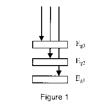
Multijunction solar cells are a proven route to higher efficiencies than
possible with single junction devices. In a multijunction solar cell, cells of
different bandgap are stacked upon one another with the highest bandgap at
the top and the lowest bandgap at the bottom. This is illustrated in Figure 1,
with E91 < E92 < E93. Light with E > E93 is absorbed in the top cell, while
light
with E < E93 passes through the top cell and impinges on the middle cell,
where light with E92 < E < E93 is absorbed and light with E < E92 passes
through the middle cell and finally light with E91 <E < E92 is absorbed in the
bottom cell. Light with E < E91 is not absorbed by any of the cells.
This strategy is a method to split up the solar spectrum into parts and
capture light more optimally from each part of the spectrum with 3 different
cells. The same strategy can be employed with just 2 cells or with more than
1
CA 02834131 2013-10-23
WO 2012/149650
PCT/CA2012/050275
3 cells. The concept of the multijunction solar cell is first described in US
Patent 2,949,498 issued August 16, 1960, entitled "Solar Energy Converter".
The stack of cells is commonly made in one of two ways. In the first
method, individual cells are made separately and mechanically stacked above
one another. This provides maximum flexibility in the design of the individual
cells. The second and very elegant method is to grow the cells monolithically
above one another (with intervening tunnel junctions for electrical
connection).
To achieve high performance, the cells are ideally single crystal layers
(grown
epitaxially) and closely lattice matched to each other.
The current state of the art cells of this type are lattice matched
Ge:(InGa)As:(InGa)P, which are now commercially available and used in
space and concentrator PV applications and recently have demonstrated
efficiencies under concentrated light exceeding 40%. In these devices the
germanium (Ge) serves as a substrate and also as the bottom cell.
In monolithic multijunction solar cells, the cells are connected in series
electrically which imposes the condition that the current flowing through them
in operation must be the same. Ideally and preferably the cells are "current
matched" by virtue of the solar illumination and the choice of the bandgaps,
if
there is latitude to adjust them.
Mechanically stacked cells are often used in 3-terminal operation (for 2
cells), since current matching is not readily obtained and separate electrical
operation maximizes power output without imposing current matching
conditions. However this approach increases costs at the system level, since
2 inverters are required for power conversion rather than one. United States
Patent 4,575,576 issued March 11, 1986 entitled "Three Junction Solar Cell"
2
CA 02834131 2013-10-23
WO 2012/149650
PCT/CA2012/050275
shows that appropriate series and parallel connections of the bottom and top
cells of monolithically grown devices allow voltage matching configurations
for
sets of cells that can be used in 2-terminal operation. Similarly, United
States
Patent 6,353,175 issued March 5, 2002 entitled "Two-terminal Cell-
interconnected-circuits using Mechanically-stacked Photovoltaic Cells
for Line-focus Concentrator Arrays" shows that appropriate series and
parallel connections of the bottom and top cells of mechanically stacked cells
allow voltage matching configurations for sets of cells that can be used in 2-
terminal operation. Voltage matched systems have some disadvantages,
including the complexity of system assembly and interconnection, as well as
difficulty in achieving a sufficiently accurate voltage matching
configuration,
because the voltages are not easily adjustable.
SUMMARY
Provided is an embodiment of a multijunction photovoltaic device
comprised of two solar cells, a bottom solar cell having an energy bandgap
with E91 and top solar cell having an energy bandgap E92, the energy
bandgaps satisfying a relationship E91 <E92, the bottom solar cell and the top
solar cell being vertically stacked and electrically interconnected in series
in
which an area of the bottom solar cell is larger than an area of the top solar
cell, in the appropriate ratio to provide for a substantially current matched
photovoltaic device for operation in a 2-terminal configuration.
Provided is an embodiment of a multijunction photovoltaic device
comprised of three solar cells, a bottom solar cell having an energy bandgap
with E91, a middle solar cell having an energy bandgap with E92 and top solar
3
CA 02834131 2013-10-23
WO 2012/149650
PCT/CA2012/050275
cell having an energy bandgap E93, the energy bandgaps satisfying a
relationship E91 < Eg< E93, the bottom solar cell, the middle solar cell and
the
top solar cell being vertically stacked and electrically interconnected in
series
in which an area of the bottom solar cell is largest, next followed by the
middle
solar cell and an area of the top solar cell is the smallest, in the
appropriate
ratio to provide for a substantially current matched photovoltaic device for
operation in a 2-terminal configuration.
Provided is an embodiment of a multijunction photovoltaic device
comprised of three solar cells, a bottom solar cell having an energy bandgap
with E91, a middle solar cell having an energy bandgap with E92 and top solar
cell having an energy bandgap E93, the energy bandgaps satisfying a
relationship E91 < Eg< E93, the bottom solar cell, the middle solar cell and
the
top solar cell being vertically stacked and electrically interconnected in
series
in which an area of the bottom solar cell is largest, next followed by the top
solar cell and an area of the middle solar cell is the smallest, in the
appropriate ratio to provide for a substantially current matched photovoltaic
device for operation in a 2-terminal configuration.
A further understanding of the functional and advantageous aspects of
the disclosure can be realized by reference to the following detailed
description and drawings.
BRIEF DESCRIPTION OF THE DRAWINGS
Embodiments will now be described, by way of example only, with
reference to the drawings, in which:
4
CA 02834131 2013-10-23
WO 2012/149650
PCT/CA2012/050275
Figure 1 shows a schematic representation of a PRIOR ART
multijunction solar cell in which cells of different bandgap are stacked upon
one another with the highest bandgap (E93) at the top and the lowest bandgap
at the bottom (E91), such that E91 < E92 < E93.
Figure 2 shows an embodiment of an areal current matched tandem
solar cell constructed in accordance with the present invention;
Figure 3 shows another embodiment of an areal current matched
tandem solar cell constructed in accordance with the present invention;
Figure 4 is a top view of the solar cell device of Figure 3, drawn
approximately to scale which shows visually that a relatively minor adjustment
in area can be used to achieve current matching;
Figure 5 is a plot which shows the theoretical maximum efficiency as a
function of areal ratio for a GaAs/Si tandem cell and the relative
contributions
of the silicon and GaAs cells.
Figure 6 is a plot which shows the theoretical maximum efficiency as a
function of areal ratio for a GaAs/Si tandem cell and the comparison of
theoretical maximum efficiency between 3-terminal and 2-terminal structures
of a GaAs/Si tandem cell.
Figure 7 is a plot which shows the 2-terminal, (InGa)P/(InGa)As/Si
triple junction cell theoretical maximum efficiency as a function of areal
ratio of
silicon solar cell to the top (InGa)P solar cell. A higher maximum efficiency
is
achieved when the area of the top (InGa)P cell is smaller than the middle
(InGa)As cell which is smaller than the bottom silicon cell, as compared to
the
case when the top (InGa)P cell and the middle (InGa)As cell areas are
reduced together relative to the bottom silicon cell.
CA 02834131 2013-10-23
WO 2012/149650
PCT/CA2012/050275
Figure 8 shows a schematic structure of a multijunction cell where
each cell has at least two subcells which have the same area as each other
but different bandgaps. The decreasing areal sequence of top, middle and
bottom cells is illustrated in this example.
Figure 9 shows a schematic structure of a multijunction cell which
comprises a top and a bottom cell, where the bottom cell has a larger area
than the top cell.
Figure 10 shows a schematic structure of a multijunction cell which
comprises a top, a middle and a bottom cell, where the bottom cell has the
largest cell area, followed by the middle cell. The top cell has the smallest
cell
area.
Figure 11 shows a schematic structure of a multijunction cell which
comprises a top, a middle and a bottom cell, where the bottom cell has the
largest cell area, followed by the top cell. The middle cell has the smallest
cell
area.
DETAILED DESCRIPTION
Various embodiments and aspects of the disclosure will be described
with reference to details discussed below. The following description and
drawings are illustrative of the disclosure and are not to be construed as
limiting the disclosure. Numerous specific details are described to provide a
thorough understanding of various embodiments of the present disclosure.
However, in certain instances, well-known or conventional details are not
described in order to provide a concise discussion of embodiments of the
present disclosure.
6
CA 02834131 2013-10-23
WO 2012/149650
PCT/CA2012/050275
As used herein, the terms, "comprises" and "comprising" are to be
construed as being inclusive and open ended, and not exclusive. Specifically,
when used in this specification including claims, the terms, "comprises" and
"comprising" and variations thereof mean the specified features, steps or
components are included. These terms are not to be interpreted to exclude
the presence of other features, steps or components.
As used herein, the term "exemplary" means "serving as an example,
instance, or illustration," and should not be construed as preferred or
advantageous over other configurations disclosed herein.
As used herein, the terms "about" and "approximately", when used in
conjunction with ranges of dimensions of particles, compositions of mixtures
or other physical, electrical or chemical properties or characteristics, are
meant to cover slight variations that may exist in the upper and lower limits
of
the ranges of dimensions so as to not exclude embodiments where on
average most of the dimensions are satisfied but where statistically
dimensions may exist outside this region. It is not the intention to exclude
embodiments such as these from the present disclosure.
The following examples are presented to enable those skilled in the art
to understand and to practice embodiments of the present disclosure. They
should not be considered as a limitation on the scope of the present
embodiments, but merely as being illustrative and representative thereof.
The specific embodiments described above have been shown by way
of example, and it should be understood that these embodiments may be
susceptible to various modifications and alternative forms. It should be
further
understood that the claims are not intended to be limited to the particular
7
CA 02834131 2013-10-23
WO 2012/149650
PCT/CA2012/050275
forms disclosed, but rather to cover all modifications, equivalents, and
alternatives falling within the spirit and scope of this disclosure.
In the standard Ge:(InGa)As:(InGa)P triple junction device, the Ge cell
provides excess current, due to its bandgap being lower than desirable
relative to the middle (InGa)As cell and top (InGa)P cell. We have made
mechanically stacked cells using (InGa)As:(InGa)P double junction devices
bonded mechanically and electrically to a bottom silicon cell. The double
junction cell could have also been a single junction cell and for simplicity
we
will refer to it as the "top cell". In this case, with silicon having a higher
bandgap than Ge and somewhat higher than desirable for current matching to
the top cells used, the silicon cell is the current limiting element of the
device.
When operated in a 2-terminal way this leads to poor efficiency, so past
efforts in this direction have all utilized 3-terminal operation.
There is a known solution to promote current matching in monolithic
multijunction cells, to maximize their output power under illumination. Kurtz,
et a/showed in a 1990 paper (Ref. 1) that when the bottom cell limits the
device current, thinning the top cell to the point that the current in the top
cell
is matched to the current in the bottom cell leads to optimal power
conversion.
In the approach described in the initial description, all light with energy
greater
than the bandgap is absorbed by the cell. However, by thinning the top cell,
some light above its bandgap goes through to the bottom cell, decreasing the
current in the top cell and increasing the current in the bottom cell, leading
to
current matching. In thin film devices such as the (InGa)As or (InGa)P cells,
this can be accomplished by adjusting the cell thickness if required, which
often requires a significant redesign of the cells. In the lattice matched
8
CA 02834131 2013-10-23
WO 2012/149650
PCT/CA2012/050275
Ge:(InGa)As:(InGa)P device, the Ge cell has excess current so this method is
not helpful to match to its current, though there is some benefit to correctly
matching the currents between the (InGa)As and (InGa)P cells. In general,
whenever a cell has excess current with respect to any cell below it, an
efficiency gain is possible by reducing the cell thickness.
In all embodiments herein stated, each "cell" has the same area and
decreasing bandgap towards the substrate with any number of subcells.
Figure 8 shows an example of two (2) subcells for each top, middle and
bottom cells where the subcells within each cell has the same area. In Figure
8, the top, middle and bottom cells are in a sequential order of increasing
cell
area as an illustration purpose. Any of these subcells could limit its
current.
Broadly, an embodiment of a solar cell constructed in accordance with
the present invention provides a multijunction photovoltaic device comprised
of two (2) solar cells: a bottom solar cell having an energy bandgap with E91
and a top solar cell having an energy bandgap E92, the energy bandgaps
satisfying a relationship E91 < E92. By "top solar cell" it is meant that this
is the
solar cell on which light is first incident and the light enters the bottom
solar
cell after passing through the top solar cell, which is why the top solar cell
is
required to have the largest bandgap. The bottom solar cell and the top solar
cell are vertically stacked and electrically interconnected in series in which
an
area of the bottom solar cell is larger than an area of the top solar cell in
an
appropriate ratio to provide for a current matched photovoltaic device for
operation in a 2-terminal configuration as shown in Figure 9.
An embodiment of a solar cell constructed in accordance with the
present invention provides a multijunction photovoltaic device comprised of
9
CA 02834131 2013-10-23
WO 2012/149650
PCT/CA2012/050275
three (3) solar cells where the bottom cell has the largest cell area, next
followed by the middle cell, and the top cell has the smallest cell area as in
Figure 10. In this example the bottom cell is the most current limiting,
followed by the middle cell.
An embodiment of a solar cell constructed in accordance with the
present invention provides a multijunction photovoltaic device comprised of
three (3) solar cells: a bottom solar cell, a middle solar cell and a top
solar cell
where the bottom cell has the largest cell area, next followed by top cell and
the middle cell has the smallest area as in Figure 11. In this example, the
bottom cell is the most current limiting, followed by the top cell.
The present invention provides multijunction solar cell devices using
advanced mechanical stacking techniques, which are also referred to as
"hybrid integrated solar cells" due to the methods used in their fabrication.
The inventors have made significant improvements over earlier mechanical
stacking approaches. The details of these improvements are disclosed in
United States Patents 4,338,480 issued July 6, 1982 entitled "Stacked
multijunction photovoltaic converters", 4,400,868 issued August 30, 1983
entitled "Method of making a transparent and electrically conductive
bond", and 5,458,694 issued October 17, 1995 entitled "Multispectral
photovoltaic component comprising a stack of cells, and method of
manufacture", the contents of which are incorporated herein in their entirety
by reference.
Example
CA 02834131 2013-10-23
WO 2012/149650
PCT/CA2012/050275
The present invention will now be illustrated using a non-limiting
example of a tandem solar cell using mechanical stacking based on a silicon
substrate with a bottom cell also in the silicon substrate. Silicon cells are
substantially less expensive than Ge substrates and the higher bandgap is
favourable in the design of higher efficiency solar cell devices. For reasons
described above, 2-terminal operation is preferred, but not easily attained
for
an arbitrary choice of a top cell. For a silicon bottom cell, a top cell with
a
bandgap of 1.68 eV would ideally be current matched. For a bandgap higher
than 1.68 eV the top cell is current limiting, while for a bandgap less than
1.68
eV the bottom (silicon) cell is current limiting.
In the silicon-based device example disclosed herein, the bottom cell is
the current limiting element, so the approach described by Kurtz, eta/could
be gainfully employed. However, the present inventors have devised a new
approach to current matching, never previously described or utilized, which is
primarily beneficial for mechanically stacked or hybrid integrated solar
cells.
This is referred to this as "areal current matching". Another way to allow
some light to circumvent the top cell and impinge on the bottom cell is to
make the top cell somewhat smaller than the bottom cell. This allows light to
impinge on the bottom cell, thereby increasing its current, while
simultaneously decreasing the current per unit area in the top cell (where the
reference area is the bottom cell area). If the area is chosen correctly, then
current matching is achieved. The inventors have demonstrated this effect
and have achieved an efficiency of 25 2% for a silicon bottom solar cell and
an (InGa)As:(InGa)P top solar cell.
11
CA 02834131 2013-10-23
WO 2012/149650
PCT/CA2012/050275
In one aspect, the tandem cell is comprised of a GaAs top cell and a
bottom silicon cell. Mechanically stacked cells that have been made with this
combination have been operated as 3-terminal devices, because the current
in the silicon cell significantly limits the performance. Calculations by the
inventors have shown that to optimize the cell performance, the GaAs cell
should absorb about 70% of the above bandgap light and allow about 30% of
the above bandgap light to pass through. Essentially the same effect is
achieved by making the GaAs cell 70% of the area of the silicon cell as
illustrated in Figures 2 and 3. Note that the larger area of the silicon cell
needs to be used as the reference area for meaningful calculation of device
efficiency. Note also that the exact placement of the open areas is not
critical
for this method to work, so either holes (as in Figure 2), grooves or a
continuous layer (as in Figure 3) would be effective as long as all parts of
the
cell are connected electrically. Note that we are assuming that the GaAs cell
allows all of the below bandgap light to pass through to the silicon cell
below,
so the GaAs cell must be sufficiently thin and/or its substrate must be highly
transparent (typically by making it lightly doped).
Figure 4 is a top view of the device of Figure 3, drawn approximately
to scale which shows visually that a relatively minor adjustment in area can
be
used to achieve current matching.
The inventors have also performed calculations to model the areal
current matching as shown in Figure 5. This shows that for equal cell area
the performance is poor, with a theoretical maximum efficiency - 20%, lower
than the theoretical maximum efficiency - 30% for either the silicon or GaAs
cells used separately. It also shows a maximum performance, with a
12
CA 02834131 2013-10-23
WO 2012/149650
PCT/CA2012/050275
theoretical maximum efficiency - 38% when the area of the silicon cell is
-1.45 times the area of the GaAs cell, in agreement with the number expected
based on 30% transmission as previously discussed.
If N1 is the current density generated by photons above the silicon
(bottom cell) bandgap and N2 is the current density generated by photons
above the GaAs (top cell) bandgap in the incident solar spectrum, then the
areal ratio of bottom cell to top cell to achieve current matching is
Abottom/Atop =
2* N2/N1 where N1- 43.8 mA/cm2 and N2- 32.0 mA/cm2, which gives
Abottom/Atop = 1.46.
Similarly if the top cells (InGa)P and (InGa)As are current matched and
of the same area, then the formula is Abottom/Atop = 1.5* N2/Nl1 where N1-
43.8
mA/cm2 and N2- 32.0 mA/cm2, which gives Abottom/Atop = 1.10, where we have
assumed that the middle cell is GaAs to determine N2. These equations can
be applied to other sets of solar cells under consideration.
In Figure 6 it is shown from calculations the result that the current
matched design achieves the same performance as the 3-terminal
performance for that design. Slightly better performance can be achieved in
pure 3-terminal operation when the areas are identical, since both cells are
more optimally illuminated, though not current matched.
In another aspect, the 3-junction tandem cell is comprised of a top
(InGa)P cell, a middle (InGa)As cell and a bottom Si cell. From the AM1.5
solar spectrum we can determine that N1- 43.8 mA/cm2, N2- 32.0 mA/cm2,
and N3- 16.9 mA/cm2, where N1 is the current density generated by photons
above the silicon (bottom cell) bandgap, N2 is the current density generated
by photons above the GaAs (middle cell) bandgap, and N3 is the current
13
CA 02834131 2013-10-23
WO 2012/149650
PCT/CA2012/050275
density generated by photons above the InGaP (top cell) bandgap. If these
cells were stacked with equal areas, the short circuit current density of each
of
the subcells would ideally be 11.8 mA/cm2, 15.1 mA/cm2 and 16.9 mA/cm2 for
the silicon, GaAs and InGaP cells respectively. The efficiency obtained from
this 3-junction tandem structure with 2-terminal configuration is far from
optimal because the current of the 3 subcells is poorly matched. The top two
cells are close to being current matched, while the silicon cell significantly
limits the current and overall device performance. Traditionally, significant
current mismatch has been addressed by using a 3-terminal device
configuration, while modest current mismatch has been addressed by thinning
down the current limiting cell to get improved performance.
Alternatively, by using the areal current matching method claimed in
this filing, the same optimal performance could be obtained without having to
resort to a 3-terminal configuration or having to accurately control the
growth
thickness of the middle and top cells with stringent requirements on their
uniformity. Current matching, with the purpose of maximizing the tandem
cell's overall efficiency, is achieved instead by adjusting the area of each
subcell. In this case, as an illustrative example, the middle (InGa)As cell
and
the top (InGa)P cell are reduced together in area with respect to the bottom
Si cell area, with the configuration shown in Figure 9 and in the simulated
results shown in Figure 7 (labeled top cell area = middle cell area). In this
case, the efficiency improves substantially over the value for equal cell
areas,
however the top and middle cells are not current matched.
Consequently, even higher efficiency can be achieved if the middle
(InGa)As cell is reduced in area with respect to the bottom Si cell area and
the
14
CA 02834131 2013-10-23
WO 2012/149650
PCT/CA2012/050275
top (InGa)P cell is further reduced in area with respect to the middle
(InGa)As
cell area with the configuration shown in Figure 10 and in the simulated
results shown in Figure 7 (labeled top cell area < middle cell area). This
configuration achieves current matching between all three cells and therefore
optimal efficiency for these three cell types.
For mechanically stacked and hybrid integrated solar cells, it is
preferred to use proper anti-reflection methods for both cells to minimize
optical losses. However, for areal current matching, the inventors note that
the considerations for anti-reflection on the exposed portion of the bottom
cell
(or cells) are different than the considerations for anti-reflection for the
overlapping regions of the two cells. In the example case given, the anti-
reflection for the exposed silicon cell is most favourably designed in the
same
way that a single junction silicon cell is designed, since both are
illuminated by
the full solar spectrum.
As mentioned above, an advantage of the present invention is that it
can be extended to more than two (2) cells and also each cell may be
composed of more than one cell. The cells can each be composed of
different materials with different bandgaps. The cells may be grown onto a
particular cell in which case the subcell areas are nominally the same and
connected in series electrically.
Another advantage is that areal current matching as disclosed herein
can mitigate cell non-idealities such as low current from the bottom cell due
to
deficiencies such as material defects, design defects such as insufficient
light
trapping, or optical losses associated with the coupling between stacked
cells.
CA 02834131 2013-10-23
WO 2012/149650
PCT/CA2012/050275
For solar cells under concentrated illumination, in general the cell
current is proportional to the illumination, while the open circuit voltage of
the
cell rises logarithmically with illumination. This is an added advantage for
concentrator cells. In areal current matching, the inventors anticipate that
the
current matching condition will nominally stay the same since all the currents
rise proportionally with illumination. However, due to cell non-idealities and
device properties, modest adjustments are expected in the ratio of areas
under concentrated light conditions. It will be appreciated by those skilled
in
the art that the areal current matching method disclosed herein can be used
to achieve optimal efficiency for a particular level of light illumination and
for a
particular solar spectrum. The solar spectrum varies from terrestrial
conditions to those above the earth's atmosphere and the device efficiency
can be optimized for those conditions using the areal current matching
method. Similarly, the solar spectrum varies with latitude, time of day and
season and atmospheric conditions and the device efficiency can be
optimized for those conditions using the areal current matching method
disclosed herein.
It will be appreciated by those skilled in the art that the areal current
matching method disclosed herein may be used alone or in combination with
other known current matching methods, such as the method of controlling the
top cell thicknesses.
As mentioned earlier, it will be appreciated that the present invention is
not restricted to silicon or other solar cell materials disclosed herein, but
it will
be understood that other materials may be used so long as the bandgap
16
CA 02834131 2013-10-23
WO 2012/149650
PCT/CA2012/050275
requirements are satisfied as decreasing from the top solar cell to the bottom
solar cell.
In summary, there is disclosed a new method for current matching of
tandem solar cells, by appropriately choosing their respective areas which
leads to favourable 2-terminal operation.
References
1. Modelling of two-junction, series connected tandem solar cells using
top-cell thickness as an adjustable parameter, S. R. Kurtz, P. Faine
and J. M. Olson, Journal of Applied Physics 68, 1890-1895 (1990).
17