Note: Descriptions are shown in the official language in which they were submitted.
CA 02836419 2015-12-16
METHOD AND APPARATUS FOR TUNING A COMMUNICATION DEVICE
Inventor(s)
Matthew R. Greene
Keith R. Manssen
Gregory Mendolia
CROSS-REFERENCE TO RELATED APPLICATIONS
[0001] The present application is a PCT International Application claiming
priority to U.S. Application Serial No. 13/108,463, filed May 16, 2011 and
U.S.
Application Serial No. 13/108,589, filed May 16, 2011.
FIELD OF THE DISCLOSURE
[0002] lbe present disclosure relates generally to communication systems,
and
more specifically to a method and apparatus for tuning a communication device.
BACKGROUND
[0003] Existing multi-frequency wireless devices (e.g., radios) use an
antenna
structure that attempts to radiate at optimum efficiency over the entire
frequency
range of operation, but can really only do so over a subset of the
frequencies. Due to
size constraints, and aesthetic design reasons, the antenna designer is forced
to
compromise the performance in some of the frequency bands. An example of such
a
wireless device could be a mobile telephone that operates over a range of
different
frequencies, such as 800 MHz to 2200 MHz, The antenna will not radiate
efficiently
at all frequencies due to the nature of the design, and the power transfer
between the
antenna, the power amplifier, and the receiver in the radio will vary
significantly.
[0004] Additionally, an antenna's performance is impacted by its operating
environment. For example, multiple use cases exist for radio handsets, which
include
such conditions as the placement of the handset's antenna next to a user's
head, or in
the user's pocket or the covering of an antenna with a hand, can significantly
impair
1
CA 02836419 2013-11-13
WO 2012/158694
PCT/US2012/037943
wireless device efficiency. Further, many existing radios use a simple circuit
composed of fixed value components that are aimed at improving the power
transfer
from power amplifier to antenna, or from the antenna to the receiver, but
since the
components used are fixed in value there is always a compromise when
attempting to
cover multiple frequency bands and multiple use cases.
[0005] Microwave devices for the propagation of electromagnetic waves
can
consist of tunable and non-tunable stages and components. The electrical path
length
of the tunable elements can be adjusted with a bias voltage. The stages and
components can be realized with microstrip geometries, stripline geometries,
coaxial
geometries slotline or fineline geometries and co-planar waveguide geometries.
The
functions of the components could be phase shifting, delaying or filtering. A
number
of components may be collected together to form a multi-stage device. This
collection can improve the bandwidth realized over a single stage microwave
device.
Stages may be put in series such as a tunable stage with a non-tunable stage.
Examples of tunable microwave devices with auto-adjusting matching circuits
are
described in U.S. Patent. No. 6,590,468 to duToit et al.
BRIEF DESCRIPTION OF THE DRAWINGS
[0006] FIG. 1 depicts an illustrative embodiment of a communication
device;
[0007] FIG. 2 depicts an illustrative embodiment of a portion of a
transceiver of
the communication device of FIG. 1;
[0008] FIGs. 3-4 depict illustrative embodiments of a tunable matching
network
of the transceiver of FIG. 2;
[0009] FIGs. 5-6 depict illustrative embodiments of a tunable reactive
element of
the tunable matching network;
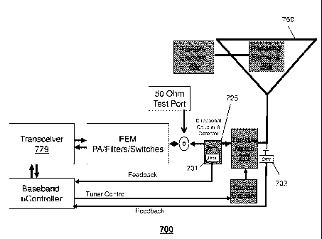
[00010] FIG. 7A depicts an illustrative embodiment of a portion of a
communication device;
[00011] FIG. 7B depicts an illustrative embodiment of another portion of a
communication device;
[00012] FIG. 8A depicts an illustrative embodiment of a portion of a multiple
antenna communication device;
2
CA 02836419 2013-11-13
WO 2012/158694
PCT/US2012/037943
[00013] FIGs. 8B-8F depict illustrative embodiments of components and
configurations for use with the embodiment of FIG. 8A;
[00014] FIGs. 9-16 depict illustrative embodiments of portions of
communication
devices;
[00015] FIG. 17 depicts an exemplary method operating in portions of one or
more
of the devices of FIGS. 1-16;
[00016] FIG. 18 depicts an illustrative embodiment of a look-up table utilized
by
one or more of the devices of FIGS. 1-6 and the method of FIG. 17; and
[00017] FIG. 19 depicts an exemplary diagrammatic representation of a machine
in
the form of a computer system within which a set of instructions, when
executed, may
cause the machine to perform any one or more of the methodologies disclosed
herein.
DETAILED DESCRIPTION
[00018] One or more of the exemplary embodiments described herein can have an
antenna with a tunable element attached to the radiating elements of the
antenna. The
tunable element can be of various types, such as a Passive Tunable Integrated
Circuit
(PTIC) having one or more electrically tunable capacitors.
[00019] In one embodiment, the antenna can be directly tuned over frequency,
moving the resonant frequency of the radiating element. By doing so, the
magnitude
of the VSWR that the antenna presents to the transceiver, can be adjusted, and
can be
kept within a range that is easier to match to the transceiver.
[00020] In another embodiment, on-antenna tuning can be combined with a
tunable
matching network such as positioned at a feed point of the antenna to achieve
greater
gains in total antenna efficiency as compared with utilizing either of these
tuning
methods separately.
[00021] In one embodiment, the tunable element on the antenna can be tuned
using
an open loop methodology, such as tuning it strictly as a function of the
band/frequency that the transceiver is operating in. In another embodiment,
other
criteria can also be used in combination with, or in place of, the
band/frequency
information, including mechanical configuration (slide up/down) or other use
cases,
and other inputs, such as proximity detector status and accelerometer position
3
CA 02836419 2013-11-13
WO 2012/158694
PCT/US2012/037943
information. The use cases can vary and can include speaker phone operation,
flipped
open and so forth.
[00022] In another embodiment, the tunable element on the antenna can be tuned
to
place the RF voltage present at a measuring component in proximity to the
antenna,
such as a detector, within a preset range. The range can be determined based
on
knowledge of the power being transmitted by the handset's transceiver, and can
be
used to establish the input impedance of the antenna within a range of Voltage
Standing Wave Ratio (VSWR) that would allow a tunable matching network, such
as
coupled at a feed point of the antenna, to improve the impedance match between
the
antenna and the transceiver. This embodiment can incorporate two separate
"loops"
of a closed loop algorithm, allowing the tunable element of the antenna to be
tuned in
a closed loop algorithm utilizing feedback from a detector, and once that loop
settled,
then the tunable matching network can be tuned using information from a
directional
coupler and the detector.
[00023] Another embodiment can utilize information from a detector and a
directional coupler in a combined closed loop algorithm. The algorithm can
simultaneously adjust the tunable element(s) on the antenna and the tunable
matching
network while also increasing the RF voltage detected at the detector subject
to the
constraints on return loss and other figure of merit parameters determined by
the
directional coupler inputs. One or more of such algorithms are described in
U.S.
Patent No. 7,991,363 to Greene. By way of example, these algorithms can
include
applying, during a transmitter time slot, a continual tuning basis to move
operation of
a transmitter towards a target and when the receive time slot is activated
adjusting to
match for the receiver frequency. The adjustment to the receiver mode of
operation
may initially involve determining the current operating conditions and
applying a
translation for tuning of the various circuits. Another algorithm can utilize
values for
the tuned components set based on operational conditions and using a look-up
table,
such as initially setting tuning values by using a look-up table and then
heuristically
fine tuning, or heuristically determining on the fly during operation. For
example,
translations applied during the receiver operation can be determined
empirically based
on a design of the circuitry and/or testing and measurements of the operation
of the
4
CA 02836419 2013-11-13
WO 2012/158694
PCT/US2012/037943
circuit. Another technique is to apply an algorithm that operates to attain a
target that
is based on one or more transmitter related metrics (such as return loss) and
the values
of the adjustable components to continuously attempt to maintain a compromised
state of operation that keeps the operation of the transmitter and the
receiver at a
particular target FOM that represents a compromise performance metric level.
[00024] Another embodiment can utilize information obtained from a detector
and/or a directional coupler using one or more of the methodologies described
in U.S.
Application Serial No. 13/005,122 to Greene. The methodologies can include
using
the derivatives or slopes of the RF voltages at the detectors responsive to
changes in
the control signals to the tunable elements. By way of example, the
methodologies
can include detecting first parameters associated with transmitting of a
communication device, such as using a directional coupler connected between a
front
end module and a matching network of a transmit/receive antenna. Based on
these
first parameters or an analysis thereof, a range of impedances for an
acceptable level
of performance of the communication device can be established and a second set
of
parameters that can be utilized for tuning. For instance, a detector
positioned at the
input of the transmit/receive antenna can detect the second parameters, such
as
changes or increases in transmitted RF power. A target impedance within the
range
of impedances can be determined using the second parameters and the matching
network for the transmit/receive antenna can be tuned based on the target
impedance.
For example, the methodology can continue to modify the matching network of
the
transmit/receive antenna to increase the detected RF voltage while
constraining the
return loss within a desired range. An offset can be applied for tuning of the
antennas
in the receive mode where the offset is based on the techniques described
above, such
as based on a translation where the frequency offset is known for the receive
mode.
[00025] In yet another embodiment, detuning of a first antenna among a
plurality
of antennas can be performed in order to reduce coupling of the first antenna
with one
or more other antennas. The detuning of the first antenna can improve the
performance of the one or more other antennas.
[00026] One embodiment of the present disclosure entails a tuning system for a
communication device having an antenna. The tuning system includes at least
one
CA 02836419 2013-11-13
WO 2012/158694
PCT/US2012/037943
first tunable element connected with at least one radiating element of the
antenna for
tuning the antenna where the adjusting of the at least one first tunable
element is
based on a closed loop process, and a matching network having at least one
second
tunable element coupled at a feed point of the antenna for tuning the matching
network based on an operational parameter of the communication device.
[00027] One embodiment of the present disclosure entails a method including
tuning an antenna of a communication device utilizing a closed loop process by
adjusting at least one first tunable element of the communication device that
is
connected with at least one radiating element of the antenna and tuning a
matching
network of the communication device by adjusting at least one second tunable
element of the matching network that is coupled to a feed point of the
antenna.
[00028] One embodiment of the present disclosure entails a tuning system for a
communication device having an antenna with a Low Band (LB) radiating element
and a High Band (HB) radiating element. The tuning system includes a plurality
of
first tunable elements, wherein at least one of the plurality of first tunable
elements
that is associated with the LB radiating element is tuned based on a desired
Voltage
Standing Wave Ratio (VSWR) associated with the antenna, and wherein at least
another of the plurality of first tunable elements that is associated with the
HB
radiating element is tuned based on increasing attenuation of an undesired
frequency.
The tuning system also includes a matching network having at least one second
tunable element coupled at a feed point of the antenna that is adjusted for
tuning the
matching network.
[00029] One embodiment of the present disclosure entails a tuning system for a
communication device having an antenna, the tuning system includes at least
one first
tunable element connected with at least one radiating element of the antenna
for
tuning the antenna where the adjusting of the at least one first tunable
element is
based on at least one of a use case associated with the communication device
and
location information associated with the communication device, and a matching
network having at least one second tunable element coupled at a feed point of
the
antenna, wherein the matching network receives control signals for adjusting
the at
least one second tunable element to tune the matching network.
6
CA 02836419 2013-11-13
WO 2012/158694
PCT/US2012/037943
[00030] One embodiment of the present disclosure entails a method including
tuning an antenna of a communication device by adjusting at least one first
tunable
element of the communication device that is connected with at least one
radiating
element of the antenna where the adjusting of the at least one first tunable
element is
based on a use case associated with the communication device, and tuning a
matching
network of the communication device by adjusting at least one second tunable
element of the matching network that is coupled between the antenna and a
transceiver of the communication device, wherein the adjusting of the second
tunable
element is a closed loop process based on an operational parameter of the
communication device.
[00031] One embodiment of the present disclosure entails a tuning system that
includes a memory and a controller. The controller is programmed to receive
antenna
efficiency information associated with one or more antennas of a group of
antennas of
a communication device, receive antenna isolation information associated with
one or
more antennas of the group of antennas, and tune at least a portion of the
group of
antennas based on the antenna efficiency information and the antenna isolation
information.
[00032] The exemplary embodiments can employ open loop tuning processes, such
as at the on-antenna tunable element and/or at the matching network. The use
cases
can include a number of different states associated with the communication
device,
such as flip-open, flip-closed, slider-in, slider-out (e.g., Qwerty or numeric
Keypad),
speaker-phone on, speaker-phone off, hands-free operation, antenna up, antenna
down, other communication modes on or off (e.g., Bluetooth/WiFi/GPS),
particular
frequency band, and/or transmit or receive mode. The use case can be based on
object or surface proximity detection (e.g., a user's hand or a table). Other
environmental effects can be included in the open loop process, such as
temperature,
pressure, velocity and/or altitude effects. The open loop process can take
into account
other information, such as associated with a particular location (e.g., in a
building or
in a city surrounded by buildings), as well as an indication of being out of
range.
[00033] The exemplary embodiments can utilize combinations of open loop and
closed loop processes, such as tuning a tunable element based on both a use
case and
7
CA 02836419 2013-11-13
WO 2012/158694
PCT/US2012/037943
a measured operating parameter (e.g., measured by a detector in proximity to
the
antenna and/or measured by a directional coupler between the matching network
and
the transceiver). In other examples, the tuning can utilize one process and
then
switch to another process, such as using closed loop tuning and then switching
to
open loop tuning based on particular factors associated with the communication
device.
[00034] FIG. 1 depicts an exemplary embodiment of a communication device 100.
The communication device 100 can comprise a wireless transceiver 102 (herein
having independent transmit and receive sections and having one or more
antennas
145 (two of which are shown in this example)), a user interface (UI) 104, a
power
supply 114, and a controller 106 for managing operations thereof. The wireless
transceiver 102 can utilize short-range or long-range wireless access
technologies
such as Bluetooth, WiFi, Digital Enhanced Cordless Telecommunications (DECT),
or
cellular communication technologies, just to mention a few. Cellular
technologies
can include, for example, CDMA-1X, WCDMA, UMTS/HSDPA, GSM/GPRS,
TDMA/EDGE, EV/DO, WiMAX, and next generation cellular wireless
communication technologies as they arise.
[00035] The UI 104 can include a depressible or touch-sensitive keypad 108
with a
navigation mechanism such as a roller ball, joystick, mouse, or navigation
disk for
manipulating operations of the communication device 100. The keypad 108 can be
an
integral part of a housing assembly of the communication device 100 or an
independent device operably coupled thereto by a tethered wireline interface
(such as
a flex cable) or a wireless interface supporting for example Bluetooth. The
keypad
108 can represent a numeric dialing keypad commonly used by phones, and/or a
Qwerty keypad with alphanumeric keys. The UI 104 can further include a display
110 such as monochrome or color LCD (Liquid Crystal Display), OLED (Organic
Light Emitting Diode) or other suitable display technology for conveying
images to
an end user of the communication device 100. In an embodiment where the
display
110 is a touch-sensitive display, a portion or all of the keypad 108 can be
presented by
way of the display.
8
CA 02836419 2013-11-13
WO 2012/158694
PCT/US2012/037943
[00036] The power supply 114 can utilize common power management
technologies (such as replaceable batteries, supply regulation technologies,
and
charging system technologies) for supplying energy to the components of the
communication device 100 to facilitate portable applications. The controller
106 can
utilize computing technologies such as a microprocessor and/or digital signal
processor (DSP) with associated storage memory such a Flash, ROM, RAM, SRAM,
DRAM or other like technologies.
[00037] The communication device 100 can utilize an on-antenna tuning element
150, which can be directly connected with the radiating element(s), including
high
band (HB) and low band (LB) radiating elements and/or a portion of the
radiating
elements. Tuning elements can be a number of components in a number of
different
configurations, including variable capacitors such as electrically tunable
capacitors,
although other tunable elements are also contemplated by the present
disclosure
including a semiconductor varactor, a micro-electro-mechanical systems (MEMS)
varactor, a MEMS switched reactive element, a piezoelectric component or a
semiconductor switched reactive element.
[00038] FIG. 2 depicts an illustrative embodiment of a portion of the wireless
transceiver 102 of the communication device 100 of FIG. 1. In GSM
applications, the
transmit and receive portions of the transceiver 102 can include common
amplifiers
201, 203 coupled to a tunable matching network 202 and an impedance load 206
by
way of a switch 204. The load 206 in the present illustration can be an
antenna as
shown in FIG. 1 (herein antenna 206). A transmit signal in the form of a radio
frequency (RF) signal (TX) can be directed to the amplifier 201 which
amplifies the
signal and directs the amplified signal to the antenna 206 by way of the
tunable
matching network 202 when switch 204 is enabled for a transmission session.
The
receive portion of the transceiver 102 can utilize a pre-amplifier 203 which
amplifies
signals received from the antenna 206 by way of the tunable matching network
202
when switch 204 is enabled for a receive session. Other configurations of FIG.
2 are
possible for other types of cellular access technologies such as CDMA. These
undisclosed configurations are contemplated by the present disclosure.
9
CA 02836419 2013-11-13
WO 2012/158694
PCT/US2012/037943
[00039] FIGs. 3-4 depict illustrative embodiments of the tunable matching
network
202 of the transceiver 102 of FIG. 2. In one embodiment, the tunable matching
network 202 can comprise a control circuit 302 and a tunable reactive element
310.
The control circuit 302 can comprise a DC-to-DC converter 304, one or more
digital
to analog converters (DACs) 306 and one or more corresponding buffers 308 to
amplify the voltage generated by each DAC. The amplified signal can be fed to
one
or more tunable reactive components 504, 506 and 508 such as shown in FIG. 5,
which depicts a possible circuit configuration for the tunable reactive
element 310. In
this illustration, the tunable reactive element 310 includes three tunable
capacitors
504-508 and an inductor 502 with a fixed inductance. Other circuit
configurations are
possible, and thereby contemplated by the present disclosure.
[00040] The tunable capacitors 504-508 can each utilize technology that
enables
tunability of the capacitance of said component. One embodiment of the tunable
capacitors 504-508 can utilize voltage or current tunable dielectric materials
such as a
composition of barium strontium titanate (BST). An illustration of a BST
composition is the Parascan Tunable Capacitor. In another embodiment, the
tunable
reactive element 310 can utilize semiconductor varactors. Other present or
next
generation methods or material compositions that can support a means for a
voltage or
current tunable reactive element are contemplated by the present disclosure.
[00041] The DC-to-DC converter 304 can receive a power signal such as 3 Volts
from the power supply 114 of the communication device 100 in FIG. 1. The DC-to-
DC converter 304 can use common technology to amplify this power signal to a
higher range (e.g., 30 Volts) such as shown. The controller 106 can supply
digital
signals to each of the DACs 306 by way of a control bus of "n" or more wires
to
individually control the capacitance of tunable capacitors 504-508, thereby
varying
the collective reactance of the tunable matching network 202. The control bus
can be
implemented with a two-wire common serial communications technology such as a
Serial Peripheral Interface (SPI) bus. With an SPI bus, the controller 106 can
submit
serialized digital signals to configure each DAC in FIG. 3 or the switches of
the
tunable reactive element 404 of FIG. 4. The control circuit 302 of FIG. 3 can
utilize
CA 02836419 2013-11-13
WO 2012/158694
PCT/US2012/037943
common digital logic to implement the SPI bus and to direct digital signals
supplied
by the controller 106 to the DACs.
[00042] In another embodiment, the tunable matching network 202 can comprise a
control circuit 402 in the form of a decoder and a tunable reactive element
404
comprising switchable reactive elements such as shown in FIG. 6. In this
embodiment, the controller 106 can supply the control circuit 402 signals via
the SPI
bus which can be decoded with common Boolean or state machine logic to
individually enable or disable the switching elements 602. The switching
elements
602 can be implemented with semiconductor switches or micro-machined switches,
such as utilized in micro-electromechanical systems (MEMS). By independently
enabling and disabling the reactive elements (capacitor or inductor) of FIG. 6
with the
switching elements 602, the collective reactance of the tunable reactive
element 404
can be varied.
[00043] The tunability of the tunable matching networks 202, 204 provides the
controller 106 a means to optimize performance parameters of the transceiver
102
such as, for example, but not limited to, transmitter power, transmitter
efficiency,
receiver sensitivity, power consumption of the communication device, a
specific
absorption rate (SAR) of energy by a human body, frequency band performance
parameters, and so on.
[00044] FIG. 7A depicts an exemplary embodiment of a portion of a
communication device 700 (such as device 100 in FIG. 1) having a tunable
matching
network which can include, or otherwise be coupled with, a number of
components
such as a directional coupler, a sensor IC , control circuitry and/or a tuner.
The
tunable matching network can include various other components in addition to,
or in
place of, the components shown, including components described above with
respect
to FIGs. 1-6. In addition to the detector 701 coupled to the directional
coupler 725,
there is shown a detector 702 coupled to the RF line feeding the antenna 750.
A
tunable matching network 775 can be coupled to the antenna 750 and a
transceiver
779 (or transmitter and/or receiver) for facilitating communication of signals
between
the communication device 700 and another device or system. In this exemplary
11
CA 02836419 2013-11-13
WO 2012/158694
PCT/US2012/037943
embodiment, the tunable match can be adjusted using all or a portion of the
detectors
for feedback to the tuning algorithm.
[00045] Various algorithms can be utilized for adjusting the matching network
750,
including utilizing Figures of Merit, which in this exemplary embodiment can
be
determined in whole or in part from measurements of the forward and reverse
signals
present at detector 701. This exemplary embodiment can also utilize detector
702 to
further improve the ability of the tuning system to enable improved
performance of
the communication device. One embodiment of the algorithm can utilize the
inputs
from detector 701 to establish a maximum return loss or VSWR for the matching
network. This method can establish a range of impedances around the targeted
impedance. This range of impedances may establish an acceptable level of
performance. Input from detector 702 can then be utilized to allow the
algorithm to
find an improved or best impedance within that acceptable range. For instance,
the
algorithm could continue to modify the matching network 775 in order to
increase the
RF voltage detected at the antenna feed, while constraining the return loss
(measured
by detector 701) to stay within the target return loss. In this embodiment,
communication device 700 can allow tuning for source impedances that are not
50
ohms. In this example, the lowest insertion loss can be chosen for the tuning
algorithm.
[00046] In another embodiment, the tuning algorithm can maintain the return
loss
while minimizing the current drain to determine desired tuning values. The
tuning
algorithm can utilize various parameters for tuning the device, including
output power
of the transmitter, return loss, received power, current drain and/or
transmitter
linearity.
[00047] Communication device 700 can include one or more radiating elements
755 of the antenna 750. One or more tunable elements 780 can be connected
directly
with one or more of the radiating elements 755 to allow for tuning of the
antenna 750
in conjunction with tuning of the matching network 775. The tunable elements
780
can be of various types as described herein, including electrically tunable
capacitors.
The number and configuration of the tunable elements 780 can be varied based
on a
number of factors, including whether the tuning is an open loop or a closed
loop
12
CA 02836419 2013-11-13
WO 2012/158694
PCT/US2012/037943
process. In one embodiment, all of the radiating elements 755 has at least one
tunable
element 780 connected thereto to allow for tuning of the radiating element. In
another
embodiment, only a portion of the radiating elements 755 have a tunable
element 780
connected thereto.
[00048] In one or more embodiments, an initial matching network stage input
can
be connected to a transmission line from the active-element portion of the
radio where
the output is the antenna feed point.
[00049] In one or more embodiments, the on-antenna tuning element can consist
of
a tunable reactive element such as a tunable capacitor (PTIC). The radiating
element
can consist of a segment of electrical conductor that is fed by the radio
circuitry, and
acts to create RF fields induced by the currents and voltage in the radiating
element as
well as the currents in the surrounding conductors near and within the same
physical
housing as the radiating element. In one or more embodiments, physically, the
on-
antenna element can either be placed in direct contact and on the same carrier
substrate as the radiating element, or it could be connected to the radiating
element by
way of connector means being in close proximity (and electrically short) to
the
radiating element.
[00050] In one or more embodiments, the initial matching network stage can be
placed proximally to the feed point or point where the RF circuitry (radio) is
connected to the radiating element, and can be electrically connected between
the
radio and the radiating element. Its purpose can be to match the impedance of
the
radiating element to that of the radio such that sufficient power is delivered
to and
from the radio from and to the base stations of the network the radio is
communicating with, although the present disclosure contemplates the matching
network being adjusted for other purposes as well.
[00051] Referring to FIG. 7B, in another exemplary embodiment that can be used
with the device of FIG. 7A, the antenna 750 and/or the radiating element(s)
755 can
be positioned on a carrier (e.g., a plastic carrier or substrate) that is
coupled with, or
otherwise connected to, a Printed Circuit Board (PCB) 740. The tunable element
or
device 780 (which in this example is a tunable capacitor) can be connected
between a
feed 741 and the antenna 750. The feed 741 can be coupled with an inductor 742
13
CA 02836419 2013-11-13
WO 2012/158694
PCT/US2012/037943
having a ground 743. In one embodiment, the inductor 742 can be one of a
printed
inductive trace or a chip inductor. In one embodiment, the antenna 750 can be
coupled with the tunable element 780 of the PCB 740 via a spring contact 743.
[00052] The example PCB 740 can be utilized with multiple tunable devices at
different points on the antenna(s). In this example, the tunable element 780
is not
exposed to the user so as to reduce the risk of damage. The example of FIG. 7C
can
be used with various types of antennas and/or with various types of tunable
elements.
In this example, by placing the tunable element 780 and the inductor 742 on
the PCB
740, the number of spring contacts can be reduced as compared to a system in
which
the tunable element and the inductor are separately positioned from the PCB.
This
example also facilitates and simplifies the manufacturing of the tunable
element
assembly. The PCB 740 provides for a more robust assembly, particularly with
respect to dropping of a mobile communication device that utilizes the PCB 740
[00053] In another exemplary embodiment, FIG. 8A depicts a portion of a
communication device 800 (such as device 100 in FIG. 1) having tunable
matching
networks for use with a multiple antenna system. In this exemplary embodiment,
there are two antennas, which are a transmit/receive antenna 805 and a
diversity
reception antenna 820. However, it should be understood that other numbers,
types
and/or configurations of antennas can be utilized with device 800. For
instance, the
antennas can be spatially diverse, pattern diverse, polarization diverse
and/or adaptive
array antennas. Tunable elements 880 can be connected with radiating elements
or a
portion thereof of the antenna 805. In another embodiment, tunable elements
880 can
be connected with multiple antennas (not shown). Tunable elements 880 allow
for
tuning and/or detuning of one or more of the antennas, including in
combination with
the tuning of the matching networks 810 and/or 825.
[00054] In one or more embodiments, the antennas can be a group of antennas
that
are placed in a fashion to adequately isolate the antennas from each other in
order to
allow them to deliver somewhat independent and uncorrelated signals to the
radio.
Their placement is determined by how they behave electrically (RF) in relation
to
each other. The particular number of antennas can vary.
14
CA 02836419 2013-11-13
WO 2012/158694
PCT/US2012/037943
[00055] In one embodiment, the antennas of communication device 800 can be
part
of a MIMO (multiple-input and multiple output) system. The multiple antennas
can
be utilized for improving communications, such as through switching or
selecting
techniques, including analyzing noise in the multiple signals and selecting
the most
appropriate signal. The multiple antennas can also be used with combining
techniques where the signals can be added together, such as equal gain
combining or
maximal-ratio combining. Other techniques for utilizing multiple signals from
multiple antennas are also contemplated by the exemplary embodiments,
including
dynamic systems that can adjust the particular techniques being utilized, such
as
selectively applying a switching technique and a combination technique. The
particular position(s) of the antenna(s) can vary and can be selected based on
a
number of factors, including being in close enough proximity to couple RF
energy
with each other.
[00056] Communication device 800 can include a number of other components
such as tunable matching networks which can include or otherwise be coupled
with a
number of components such as directional couplers, sensor ICs, bias control
and other
control ICs and tunable matching networks. The tunable matching networks can
include various other components in addition to, or in place of the components
shown,
including components described above with respect to FIGs. 1-7. This example
also
includes a transceiver 850 of the communication device 800 that includes
multiple
receivers and/or transmitters for the multiple antennas 805 and 820 to serve
the
purpose of diversity reception.
[00057] In one embodiment, a first tunable matching network 810 can be coupled
at the input to the transmit/receive antenna 805 and a second tunable matching
network 825 can be coupled to the input to the diversity reception antenna
820. Both
of these matching networks 810 and 825 can be adjusted (e.g., tuned) to
improve
performance of the communication device 800 in response to changes in bands,
frequencies of operation, physical use cases and/or proximity of the antennas
805 and
820 to the user or other objects which can affect the impedances presented by
the
antennas to the Front End Module (FEM) 860 and transceiver 850. In one
embodiment, the feedback line could be removed, such as by using the FEM to
route
CA 02836419 2013-11-13
WO 2012/158694
PCT/US2012/037943
these signals appropriately to perform these measurements (e.g., avoiding
filtering out
the signals).
[00058] Tunable matching network 810 can be adjusted using different methods
and/or components. In one embodiment, a detector 830 can be coupled to the
device
800 so as to detect RF voltage present at the connection to the diversity
reception
antenna 820. Received power levels at this point may be below -50 dBm. Some
detectors, such as a diode detector or a logarithmic amplifier, may not
typically be
adequate to detect such levels. However, since in this exemplary embodiment,
the
two antennas 805 and 820 are in the same device 800 and in proximity to each
other,
they can inherently couple RF energy from one antenna to the other. While the
communication device 800 does not require this coupling, its presence can be
utilized
by the exemplary embodiments for the purposes of tuning the antenna matching
networks. In one example, after establishing the tuning state for the
diversity match at
the transmit frequency, a predetermined relationship or offset can be applied
to the
matching network 825 in order to adjust the match to the receiver operating
frequency.
[00059] Communication device 800 can include other components and
configurations for determining, or otherwise measuring, parameters to obtain
the
desired tuning. Various configurations are illustrated in FIGS. 8B-8F. FIG. 8B
illustrates a capacitive coupling configuration between the tunable matching
network
and the FEM. FIG. 8C illustrates a resistive coupling between the tunable
matching
network and the FEM for obtaining the desired parameters. The FEM 860 in the
diversity path of the communication device 800 may be highly reflective at the
transmission frequency. This can create a standing wave and the detector may
be at a
voltage minimum causing detection to be made more difficult for the capacitive
and
resistive couplings shown in FIGS. 8A and 8B. In FIG. 8D, a directional
coupler can
be utilized to sample only the forward power, which allows for obtaining the
desired
parameters despite the existence of any standing wave in the diversity path.
FIGS. 8E
and 8F utilize detectors, but sample multiple points along the path to avoid
sampling
at a voltage minimum.
16
CA 02836419 2013-11-13
WO 2012/158694
PCT/US2012/037943
[00060] In one embodiment, the tunable match on the transmit/receive antenna
805
can be tuned similar to the technique described above with respect to FIG. 7A
but
instead of using detector 815, detector 830 can be used to measure increases
in
transmitted RF power coupled to the diversity reception antenna 820. As such,
detector 815 (shown in broken lines in FIG. 8A) can be removed from the device
800,
thereby reducing the cost and complexity. Thus, this example would tune both
antennas utilizing only one detector (e.g., detector 830) coupled with one of
the
antennas (e.g., the diversity reception antenna 820) and without another
detector
coupled to the other antenna. This example relies upon a fairly constant
coupling
coefficient between the two antennas at any particular band, frequency and use
case,
and for any operation of the algorithm these may all be considered constant.
[00061] In another embodiment, after tunable matching network 810 is adjusted
by
the algorithm, tunable matching network 825 can also be adjusted. By measuring
the
coupled transmitted power present at detector 830, the tunable matching
network 825
can be adjusted to increase coupled transmitter power seen at detector 830. In
one
example, after establishing the tuning state for the diversity match at the
transmit
frequency, a predetermined relationship or offset can be applied to the
matching
network 825 in order to adjust the match to the receiver operating frequency.
For
instance, the tuning circuits can be adjusted initially based on transmitter
oriented
metrics and then a predetermined relationship or offset can be applied to
attain a
desired tuning state for both transmitter and receiver operation. In another
embodiment, the operational metric can be one or more of transmitter
reflection loss,
output power of the transmitter, current drain and/or transmitter linearity.
[00062] For example, in a time division multiplexed (TDM) system in which the
transmitter and the receiver operate at different frequencies but only operate
in their
respective time slots (i.e., transmit time slot and receive time slot), this
can be
accomplished by identifying an optimal tuning for the transmitter and then
adding an
empirically derived adjustment to the tuning circuits in receive mode. As
another
example, in a frequency division multiplexed (FDM) system in which the
transmitter
and receiver operate simultaneously and at different frequencies, this can be
accomplished by identifying a target operation for the transmitter, and then
adjusting
17
CA 02836419 2013-11-13
WO 2012/158694
PCT/US2012/037943
the tuning circuits first to the target value for the transmitter and then
adjusting the
values to approach a compromised value proximate to an equal or desired target
value
for the receiver. In one embodiment, a predetermined relationship, (e.g., an
offset,
scaling factor, translation or other change or modification) can be applied to
the
adjustments of the variable components when switching from the transmit mode
to the
receive mode. This translation can be a function of the values obtained while
adjusting during the transmit time slot. The translation can then be removed
upon
return to the transmitter mode and the adjustment process is resumed. In one
embodiment, because any frequency offset between the transmit signal and the
receive signal is known, an adjustment or modification of the setting of the
matching
network in the form of a translation or some other function can be applied to
the
matching network during the receive time slot. In another embodiment, the
adjustment can be performed in multiple steps if the transmission and
reception
frequencies are far apart.
[00063] In another embodiment, a Figure of Merit can be utilized that not only
incorporates the transmit metrics, but also incorporates an element to attain
a
compromise between optimal transmitter and optimal receiver operation. This
can be
accomplished by identifying a target operation goal, such as a desired
transmitter and
receiver reflection loss and then identifying an operational setting that is a
close
compromise between the two. This embodiment thus can incorporate not only
transmitter metrics but also tuning circuit settings or preferences into the
algorithm.
The tuning preferences can be empirically identified to ensure the desired
operation.
[00064] In one embodiment where the communication device 800 employs antenna
diversity for receive operation but does not employ antenna diversity for
transmit
operation, antenna 820 would be receive only. The transceiver can transmit on
antenna 805 and can receive on both antennas 805 and 820. For adaptive closed
loop
tuning of the tunable matching network 825 on the diversity antenna, the
communication device 800 can obtain a metric indicating the performance of the
tunable matching circuit at the receive frequency. The metric can be used to
tune the
match to adjust the performance at the receive frequency. This can be done by
measuring the level of the received signal using the receiver in the
transceiver IC.
18
CA 02836419 2013-11-13
WO 2012/158694
PCT/US2012/037943
This measurement is known as RSSI, received signal strength indicator. An RSSI
measurement can be very noisy and unstable due to highly variable impairments
in
the propagation channel, such as fading. These variations can be filtered
using
averaging. However, the amount of averaging necessary could make such a
measurement prohibitively slow and not suitable as feedback for closed loop
antenna
tuning.
[00065] In this embodiment, the transmit signal is moderately coupled to the
tunable match in the diversity path because the main antenna and the diversity
antenna are located on the same communications device. The main antenna and
the
diversity antenna may only have 20dB isolation in many cases. The transmit
signal
present at tunable match 825 may be a much stronger and more stable signal
than the
receive signal present at tunable matching network 825. The transmit signal
can be
used to make reliable measurements that can be used for closed loop tuning.
[00066] The transmit signal can be measured using detector 830. The detector
can
be placed between the tunable match and the transceiver. This is effectively
the
output of the tunable match. A directional coupler is not necessary for this
measurement in this embodiment, and capacitive or resistive coupling may be
used, as
long as the detector has sufficient dynamic range. Other components and
configurations of the components can also be utilized for the parameter
detection,
such as shown in U.S. Patent Publication No. 20090039976 by McKinzie,
including
the use of a multi-port RF matching network with a diplexer for signal routing
among
ports, a voltage divider with a diode detector, a resistive voltage divider
using a multi-
pole RF switch, a shunt RF branch having a series string of capacitors that
enables
tapping into various nodes along the string, a bias driving circuit for
providing a bias
signal to a reactive element, and so forth.
[00067] In this embodiment, maximizing the output voltage of a tunable match
can
be the equivalent to minimizing insertion loss, and for a lossless network it
can be
equivalent to minimizing mismatch loss. An alternative to using detector 830
is to
use the receiver itself (tuned to the transmit frequency) to measure the
transmit signal.
These are a few viable methods for measuring the transmit signal through the
19
CA 02836419 2013-11-13
WO 2012/158694
PCT/US2012/037943
diversity tunable match. Other forms of signal detection are contemplated by
the
present disclosure.
[00068] A complication with using the transmit signal for tuning can be that
it is at
a different frequency than the receive signal and the objective of the tunable
match in
the diversity path is to adjust performance at the receive frequency. In one
exemplary
method, the tunable matching circuit is adjusted for reception performance
based on
transmission measurements. In this exemplary method, a tunable match can be
optimized at the transmit frequency using measurements on the transmit signal
and
then the matching circuit can be adjusted using a predetermined relationship
between
the transmit settings and the receive settings to provide the desired
performance at the
receive frequency.
[00069] In one embodiment that utilizes a tunable matching network which
contains two tunable capacitors, one set of tuning values, designated (C1TX,
C2TX),
can be applied only during the measurement of the transmit signal. The other
set of
tuning values, designated (C1RX, C2RX), can be applied in between the transmit
measurements. This embodiment describes two tunable capacitors, but this
exemplary embodiment can apply to various numbers and types of tunable
elements.
In this embodiment, the Rx tuning values are a function of the Tx tuning
values. As
the Tx values adaptively change throughout the iterative algorithm, the Rx
values will
also change, tracking the Tx values with a predetermined relationship. If the
figure of
merit is set to maximize Vout, the Tx solution can converge at (C1TXopt,
C2TXopt),
and can be appropriately adjusted using the predetermined relationship to
(C1RXopt,
C2RXopt) to achieve the desired RX performance.
[00070] Each time the tunable match is set to (C1TX, C2TX) in order to perform
a
Tx measurement, the performance at the Rx frequency may be degraded during the
time that (C1TX, C2TX) is applied. It is desirable in this embodiment to
perform the
measurement as quickly as possible to minimize the Rx degradation caused by Tx
tuning during the measurement. In one embodiment, the Tx values can be applied
for
less than one percent of the time while still achieving adequate convergence
time.
[00071] In one embodiment, the relationship between the TX and RX tuning
solutions can be dependent upon the bands of operation, and in the case where
the
CA 02836419 2013-11-13
WO 2012/158694
PCT/US2012/037943
receiver is tuned to monitor signals in an alternate band, then an alternate
tuning
solution (C1RX2, C2RX2) can be applied during that measurement.
[00072] Another exemplary method for controlling the tuning can be employed,
which does not require setting the tunable capacitors to values optimized for
transmission while performing the Tx measurement. The objective is to operate
the
tuning matching network at settings that optimize Rx performance. These
settings are
at capacitance values that are a specific amount away from the Tx optimum in a
specific direction. An algorithm can be utilized that will find this location
in the
capacitance plane without first needing to find the Tx optimum. The Tx level
can
change based on a number of circumstances, such as from power control commands
in the transceiver or from variations in supply voltage, temperature,
component
tolerances, and so forth. In this embodiment, since only measurement of the
output
RF voltage of the tuner is being performed, a determination may not be made as
to
whether the algorithm is at the Tx optimum or a specific amount away from the
Tx
optimum because the Tx level is changing. This may prevent the use of an
algorithm
that simply targets a specific Tx signal level.
[00073] A metric that can be useful in determining where the tuning matching
network is operating relative to the Tx optimum is to utilize the slope, or
derivative of
the Tx level with respect to the value or setting of the tunable capacitors
(or other
types of tunable elements). If the RF voltage (Vout) present at the output of
the
tunable match at the TX frequency is determined, such as through use of a log
detector, then the first derivatives are dVout/dC1 and dVout/dC2. These
derivatives
can be calculated using the finite difference of two sequential measurements.
These
slopes will be a function of the tunable capacitors. These slopes will not be
a function
of the absolute power level of the Tx signal since a log detector is being
utilized. If a
log detector or its equivalent is not utilized, the logarithm of the Tx
voltage can be
calculated prior to calculating the slope. By defining a Figure of Merit that
includes
dVout/dC1 and dVout/dC2, the algorithm can converge to a solution that is a
specific
amount away from the Tx optimum in a specific direction, in this case near the
Rx
optimum. In this embodiment, a log detector is a device having a logarithmic
response.
21
CA 02836419 2013-11-13
WO 2012/158694
PCT/US2012/037943
[00074] In some cases, specifying the slopes alone will not result in a unique
solution (i.e., there may be multiple solutions). The algorithm can resolve
this
situation by adding a PTC preference to the Figure of Merit. A tunable match
may
have many solutions that meet a Tx RL goal and a PTC preference can be
included in
the Figure of Merit to identify a solution that not only meets the Tx RL goal
but also
meets an Rx performance goal. Similarly, a tunable match may have many
solutions
that meet a slope criteria and a PTC preference can be included in the Figure
of Merit
to identify a solution that not only meets the slope criteria but also meets
an Rx
performance goal.
[00075] In cases where using dVout alone results in multiple solutions, it is
also
possible to use the second derivative to resolve these cases. For example,
second
derivatives (d2Vout/dC2dC1) can be utilized, which is dVout/dC2 differentiated
with
respect to C1. Specifying dVout/dC2 and d2Vout/dC2dC1 can identify the correct
or
desired Rx solution from the multiple solutions. This exemplary method can
include
determining derivative information (e.g., one or more of a first derivative,
and/or a
second derivative, and/or etc.) associated with the RF voltage based on
derivatives of
the RF voltage and the variable capacitance values, and tuning the tunable
matching
network using the derivative information.
[00076] Another exemplary embodiment can use detector 830 of the
communication device 800 in the diversity path as feedback to adjust tunable
matching network 810 on the main antenna 805. The tunable matching network 810
coupled with the main antenna has both transmit and receive signals, and can
be
optimized for Tx performance, Rx performance, and Duplex performance. For the
Tx solution, Vout can be maximized. For the Rx solution and the Duplex
solution,
dVout can be included in the Figure of Merit. A PTC preference may be required
to
identify the optimal Rx solution but is not required to identify the optimal
duplex
solution. , return loss, received power, current drain or transmitter
linearity
[00077] In one or more exemplary embodiments, the Figure of Merit may be
constructed such that when it equals a certain value, or is minimized or
maximized,
the desired tuner settings are achieved. The Figure of Merit may be used with
a
number of different optimization algorithms. For example, a more exhaustive
22
CA 02836419 2013-11-13
WO 2012/158694
PCT/US2012/037943
approach may be used that evaluates the Figure of Merit at every combination
of
capacitor values. Other suitable algorithms can also be utilized, including a
simplex
algorithm, a binary search algorithm, and/or a gradient algorithm.
[00078] In another embodiment, communication device 800 can tune antennas 805
and 820 without using detectors 815 and 830. The tunable matching network 810
can
be adjusted using several different methods. After the tunable matching
network 810
is adjusted, the tunable matching network 825 can be adjusted. By monitoring
the
detector 801 coupled to the directional coupler 875, the diversity match
tuning state
can be determined which adjusts the tunable matching network 825 to the
transmit
frequency. If significant coupling between the two antennas 805 and 820 is
assumed,
and by monitoring the return loss of the transmit/receive match while
adjusting the
diversity reception antenna 820 match during transmitting, the diversity match
tuning
state can be determined which tunes the diversity reception antenna 820 to the
transmit frequency. This tuning state can minimize the return loss at the
transmit
frequency as measured at the directional coupler 875. After finding this
tuning state
the tunable matching network 825 can then be adjusted (e.g., offset)
appropriately for
the receive frequency.
[00079] In another embodiment depicted in FIG. 9, communication device 900
includes tunable element 902 for tuning antenna 901. The tuning can be in an
open-
loop manner, such as based on frequency and/or use case. Tunable element 902
can
be adjusted such that the antenna VSWR is in a range that can be reasonably
matched
by tunable matching network 908.
[00080] Tunable element 902 can be adjusted in an open-loop manner to maximize
rejection or attenuation at an unwanted frequency while maintaining the VSWR
at the
fundamental frequency in the range that can be reasonably matched by the
tunable
matching network 908. The unwanted frequency may be a harmonic or an
interferer.
Matching network 908 can be tuned in a closed-loop manner, such as based on
operational parameter(s) collected from detector 903 and/or directional
coupler 905
having forward and reverse detectors 906, 907 positioned between the matching
network 908 and the transceiver 909.
23
CA 02836419 2013-11-13
WO 2012/158694
PCT/US2012/037943
[00081] In another embodiment depicted in FIG. 10, communication device 1000
includes tunable element 1002 for tuning antenna 1001 in an open-loop manner
based
on frequency and/or use case. Tunable element 1002 can be tuned such that the
antenna VSWR is in the range that can be reasonably matched by tunable
matching
network 1008, and the on-antenna tuning can maximize rejection or attenuation
at an
unwanted frequency while maintaining a VSWR at the fundamental frequency in
the
range that can be reasonably matched by tunable matching network 1008. The
tunable matching network can be tuned based on metrics gathered from detector
1003
without utilizing measurements from any measuring device in between the
matching
network and the transceiver 1009.
[00082] In another embodiment depicted in FIG. 11, communication device 1100
includes tunable element 1102 for tuning antenna 1101 in a closed loop manner
while
also tuning the matching network 1108 in a closed-loop manner. A directional
coupler 1105 having forward and reverse detectors 1106, 1107 can be connected
between the matching network 1108 and a transceiver 1109 for obtaining
operational
parameter(s) for performing the closed loop tuning of element(s) 1102 and
matching
network 1108. Tuning can be performed in this embodiment without obtaining
measurements from a measuring component in proximity to the antenna.
[00083] In another embodiment depicted in FIG. 12, communication device 1200
includes tunable element 1202 for tuning antenna 1201 in a closed loop manner
based
on maintaining the RF voltage present at detector 1203 in a preset range
relative to the
transmit power. This can establish an antenna impedance that is in the range
that can
be reasonably matched by tunable matching network 1208. Matching network 1208
can be tuned in a closed loop manner based on operational parameter(s)
obtained
using directional coupler 1205 having forward and reverse detectors 1206, 1207
coupled with the device 1200 between the matching network and the transceiver
1209.
[00084] In another embodiment depicted in FIG. 13, communication device 1300
includes tunable element 1302 for tuning antenna 1301 in a closed loop manner
based
on the RF voltage obtained at detector 1303, such as maintaining the RF
voltage in a
preset range relative to the transmit power. Matching network 1308 can be
tuned in a
24
CA 02836419 2013-11-13
WO 2012/158694
PCT/US2012/037943
closed loop manner based on operational parameter(s) obtained using detector
1303
without obtaining measurements from any measuring components coupled between
the matching network 1308 and the transceiver 1309.
[00085] In another embodiment depicted in FIG. 14, communication device 1400
includes tunable element 1402 for tuning antenna 1401 in a closed loop manner
by
placing the antenna VSWR detected using directional coupler 1410 with forward
and
reverse detectors 1411, 1412 in a preset range. This will establish an antenna
VSWR
that is in the range which can then be reasonably matched by tunable matching
network 1408. Within the acceptable range of the antenna VSWR, the solution
can be
biased using a tuning preference for on-antenna element 1402 to achieve a
second
criteria. Matching for the element 1402 can be performed at the Rx frequency
and/or
based on achieving linearity. The matching network 1408 can be tuned in a
closed
loop manner based on operational parameter(s) obtained from the directional
coupler
1405 having forward and reverse detectors 1406, 1407 positioned between the
matching network and the transceiver 1409.
[00086] In another embodiment depicted in FIG. 15, communication device 1500
includes tunable element 1502 for tuning antenna 1501 in a closed loop manner
by
placing the antenna VSWR detected using directional coupler 1510 with forward
and
reverse detectors 1511, 1512 in a preset range. This will establish an antenna
VSWR
that is in the range which can then be reasonably matched by tunable matching
network 1508. Within the acceptable range of the antenna VSWR, the solution
can be
biased using a tuning preference for on-antenna tunable element 1502 to
achieve a
second criteria. Matching for the element 1502 can be performed at the Rx
frequency
and/or based on achieving linearity. The matching network 1508 can be tuned in
a
closed loop manner based on operational parameter(s) obtained from the
detector
1503 coupled in proximity to the antenna 1501 without obtaining measurements
from
any measuring component positioned between the matching network and the
transceiver 1509.
[00087] In another embodiment depicted in FIG. 16, communication device 1600
includes tunable element 1602 and tunable element 1610 for tuning antenna
1601.
Tunable element 1602 can primarily affect the LB radiator and tunable element
1610
CA 02836419 2013-11-13
WO 2012/158694
PCT/US2012/037943
can primarily affect the HB radiator of the antenna 1601. Tunable element 1602
can
be adjusted in an open-loop manner based on frequency and/or use case. Tunable
element 1602 can be adjusted such that the antenna VSWR as determined from
metrics of the detector 1603 is in a range that can be reasonably matched by
tunable
matching network 1608. Tunable element 1610 can be adjusted in an open-loop
manner to maximize rejection or attenuation at an unwanted frequency while
maintaining a VSWR at the fundamental frequency in the range that can be
reasonably matched by tunable matching network 1608. The unwanted frequency
may be a harmonic, such as in the High Band, while the fundamental (TX & RX)
frequencies can be in the Low Band. Matching network 1608 can be tuned in a
closed
loop manner utilizing operational parameter(s) obtained from the directional
coupler
1605 having forward and reverse detectors 1606, 1607 coupled between the
matching
network and the transceiver 1609.
[00088] Another embodiment provides for tuning one or more of the antennas of
a
communication device. In a multiple antenna system, simply maximizing the over
the
air efficiency of all the antennas may not accomplish the best overall
performance of
the communication system. The isolation or de-correlation between antennas in
a
small handset is also a key parameter in defining the overall performance. A
control
method that considers the efficiency of both antennas and the isolation
between them
is advantageous. For example, in an antenna diversity system, the antennas can
be
tuned so as to reduce coupling between the antennas without degrading the
efficiency
of either antenna, or to degrade efficiency minimally such that overall system
performance is enhanced. Thus, even for closely spaced antennas in a handheld
mobile application, the coupling can be kept to a minimum in spite of antenna
proximity. Other parameters other than antenna cross-coupling may also be
optimized
to improve overall performance of the system, such as in a MIMO system where
there
can be simultaneously multiple output antennas and multiple input antennas.
[00089] FIG. 17 depicts an exemplary method 1700 operating in portions of one
or
more of the devices of FIGs. 1-16. Method 1700 can be utilized with
communication
devices of various configurations, including multiple antenna devices. Method
1700
can begin with step 1702 by detecting one or more parameters of the
communication
26
CA 02836419 2013-11-13
WO 2012/158694
PCT/US2012/037943
device, such as parameters associated with transmitting that are obtained
through use
of measuring components including a detector and/or a directional coupler. The
number and positioning of the measuring components can vary and can be in
proximity to the antenna and/or between a matching network and a transceiver.
[00090] In step 1704, it can be determined whether there are multiple on-
antenna
tuning elements. If there are more than one such tuning elements then in step
1706
tuning elements associated with the LB radiating element(s) can be tuned based
on a
desired VSWR. In step 1708, tuning elements associated with the HB radiating
element(s) can be tuned based on a different factor, such as a rejection or
attenuation
of an unwanted frequency. If on the other hand, there is only one on-antenna
tuning
element and/or the tuning elements are only connected with one of the LB or HB
radiating elements of the antenna then method 1700 can proceed to step 1710
where
the on-antenna tuning element(s) is tuned using an open loop and/or closed
loop
process. The open loop process can utilize various factors to determine
tuning,
including use case, operating frequency, proximity information
accelerometer/position information, and so forth. The closed loop process can
utilize
various factors to determine tuning, including RF voltage, return loss,
received power,
current drain and/or transmitter linearity
[00091] In step 1712, tuning can be performed utilizing the matching network.
The
tuning of the matching network can be an open loop and/or closed loop process,
including using one or more of the factors described above with respect to the
open
and closed loop processes that can tune the on-antenna tuning elements. The
timing
of the tuning utilizing the matching network can vary, including being
performed
simultaneously with tuning of the on-antenna tuning elements, after tuning of
the on-
antenna tuning elements and/or before tuning of the on-antenna tuning
elements.
Method 1700 can be an iterative process that tunes the on-antenna tuning
elements
and/or the matching network.
[00092] In one embodiment, the tuning of the matching network(s) can be
performed in combination with look¨up tables such as shown in FIG. 18. For
instance, one or more desirable performance characteristics of a communication
device 100 can be defined in the form of Figures of Merits (F0M5), the
27
CA 02836419 2013-11-13
WO 2012/158694
PCT/US2012/037943
communication device can be adapted to find a range of tuning states that
achieve the
desired FOMs by sweeping a mathematical model in fine increments to find
global
optimal performance with respect to the desired FOMs. In one embodiment, look-
up
table 1800 can be indexed (e.g., by the controller 106 of the communication
device
100 of FIG. 1) during operation according to band and/or use case.
[00093] From the foregoing descriptions, it would be evident to an artisan
with
ordinary skill in the art that the aforementioned embodiments can be modified,
reduced, or enhanced without departing from the scope and spirit of the claims
described below. For example, detector 830 may include a directional coupler
for the
diversity antenna to compensate for out-of-band impedance of the Rx filter
that may
create a very high standing wave on the feed line and put voltage nulls at
unpredictable places on the line (including at the base of the antenna).
[00094] In another embodiment, combinations of open and closed loop processes
can be utilized for tuning of one or more of the tunable elements of the
antenna and/or
the matching network. For instance, a tunable element of the antenna can be
tuned in
part with a closed loop process based on an operational parameter of the
communication system and in part with an open loop process based on a use case
and/or location information of the communication device. In another
embodiment,
the sue of closed loop and open loop process can be alternated or otherwise
arranged
in being applied to a particular tunable element, such as initially applying
an open
loop process but then later applying a closed loop process, including
switching from
an open loop to a closed loop process based on operational parameters of the
communication device. In another embodiment, the matching network can be tuned
in whole or in part using an open loop process, such as based on a use case
provided
in a look-up table and/or based on location information associated with the
communication device.
[00095] The exemplary embodiments can employ open loop tuning processes, such
as at the on-antenna tunable element and/or at the matching network. The use
cases
can include a number of different states or status associated with the
communication
device, such as flip-open, flip-closed, slider-in, slider-out (e.g., Qwerty or
numeric
Keypad), speaker-phone on, speaker-phone off, hands-free operation, antenna
up,
28
CA 02836419 2013-11-13
WO 2012/158694
PCT/US2012/037943
antenna down, other communication modes on or off (e.g., Bluetooth/WiFi/GPS),
particular frequency band, and/or transmit or receive mode. The use case can
be
based on object or surface proximity detection (e.g., a user's hand or a
table). Other
environmental effects can be included in the open loop process, such as
temperature,
pressure, velocity and/or altitude effects. The open loop process can take
into account
other information, such as associated with a particular location (e.g., in a
building or
in a city surrounded by buildings), as well as an indication of being out of
range. The
exemplary embodiments can utilize combinations of open loop and closed loop
processes, such as tuning a tunable element based on both a use case and a
measured
operating parameter (e.g., measured by a detector in proximity to the antenna
and/or
measured by a directional coupler between the matching network and the
transceiver).
In other examples, the tuning can utilize one process and then switch to
another
process, such as using closed loop tuning and then switching to open loop
tuning
based on particular factors associated with the communication device. The use
case
can be based on the knowledge of transmitter power level setting and receiver
received signal strength, current drain, accelerometer direction/orientation,
and any
other information that is available within the device (e.g., a handset,
tablet, or other
wireless communication device) indicative of operating modes or use case.
[00096] In one embodiment, Low Band (LB) radiating element(s) and High Band
(HB) radiating element(s) can be utilized with the antenna, where at least one
tunable
element is associated with the LB radiating element is tuned based on a
desired
Voltage Standing Wave Ratio (VSWR) associated with the antenna, and wherein at
least another tunable elements that is associated with the HB radiating
element is
tuned based on a different performance metric. The different performance
metric can
be based on attenuation of an undesired frequency. As an example, the
undesired
frequency can be a harmonic frequency or can be associated with an interferer.
[00097] Methodologies and/or components that are described herein with respect
to
tuning of one tunable element can also be utilized with respect to tuning of
other
tunable elements. For example, derivative information utilized for tuning the
matching network can be used for tuning of on-antenna tunable elements.
29
CA 02836419 2013-11-13
WO 2012/158694
PCT/US2012/037943
[00098] Other suitable modifications can be applied to the present disclosure.
Accordingly, the reader is directed to the claims for a fuller understanding
of the
breadth and scope of the present disclosure.
[00099] FIG. 19 depicts an exemplary diagrammatic representation of a machine
in
the form of a computer system 1900 within which a set of instructions, when
executed, may cause the machine to perform any one or more of the
methodologies
discussed above. In some embodiments, the machine operates as a standalone
device.
In some embodiments, the machine may be connected (e.g., using a network) to
other
machines. In a networked deployment, the machine may operate in the capacity
of a
server or a client user machine in server-client user network environment, or
as a peer
machine in a peer-to-peer (or distributed) network environment.
[000100] The machine may comprise a server computer, a client user computer, a
personal computer (PC), a tablet PC, a laptop computer, a desktop computer, a
control
system, a network router, switch or bridge, or any machine capable of
executing a set
of instructions (sequential or otherwise) that specify actions to be taken by
that
machine. It will be understood that a device of the present disclosure
includes
broadly any electronic device that provides voice, video or data
communication.
Further, while a single machine is illustrated, the term "machine" shall also
be taken
to include any collection of machines that individually or jointly execute a
set (or
multiple sets) of instructions to perform any one or more of the methodologies
discussed herein.
[000101] The computer system 1900 may include a processor 1902 (e.g., a
central
processing unit (CPU), a graphics processing unit (GPU, or both), a main
memory
1904 and a static memory 1906, which communicate with each other via a bus
1908.
The computer system 1900 may further include a video display unit 1910 (e.g.,
a
liquid crystal display (LCD), a flat panel, a solid state display, or a
cathode ray tube
(CRT)). The computer system 1900 may include an input device 1912 (e.g., a
keyboard), a cursor control device 1914 (e.g., a mouse), a disk drive unit
1916, a
signal generation device 1918 (e.g., a speaker or remote control) and a
network
interface device 1920.
CA 02836419 2013-11-13
WO 2012/158694
PCT/US2012/037943
[000102] The disk drive unit 1916 may include a machine-readable medium 1922
on
which is stored one or more sets of instructions (e.g., software 1924)
embodying any
one or more of the methodologies or functions described herein, including
those
methods illustrated above. The instructions 1924 may also reside, completely
or at
least partially, within the main memory 1904, the static memory 1906, and/or
within
the processor 1902 during execution thereof by the computer system 1900. The
main
memory 1904 and the processor 1902 also may constitute machine-readable media.
[000103] Dedicated hardware implementations including, but not limited to,
application specific integrated circuits, programmable logic arrays and other
hardware
devices can likewise be constructed to implement the methods described herein.
Applications that may include the apparatus and systems of various embodiments
broadly include a variety of electronic and computer systems. Some embodiments
implement functions in two or more specific interconnected hardware modules or
devices with related control and data signals communicated between and through
the
modules, or as portions of an application-specific integrated circuit. Thus,
the
example system is applicable to software, firmware, and hardware
implementations.
[000104] In accordance with various embodiments of the present disclosure, the
methods described herein are intended for operation as software programs
running on
a computer processor. Furthermore, software implementations can include, but
not
limited to, distributed processing or component/object distributed processing,
parallel
processing, or virtual machine processing can also be constructed to implement
the
methods described herein.
[000105] The present disclosure contemplates a machine readable medium
containing instructions 1924, or that which receives and executes instructions
1924
from a propagated signal so that a device connected to a network environment
1926
can send or receive voice, video or data, and to communicate over the network
1926
using the instructions 1924. The instructions 1924 may further be transmitted
or
received over a network 1926 via the network interface device 1920.
[000106] While the machine-readable medium 1922 is shown in an example
embodiment to be a single medium, the term "machine-readable medium" should be
taken to include a single medium or multiple media (e.g., a centralized or
distributed
31
CA 02836419 2013-11-13
WO 2012/158694
PCT/US2012/037943
database, and/or associated caches and servers) that store the one or more
sets of
instructions. The term "machine-readable medium" shall also be taken to
include any
medium that is capable of storing, encoding or carrying a set of instructions
for
execution by the machine and that cause the machine to perform any one or more
of
the methodologies of the present disclosure.
[000107] The term "machine-readable medium" shall accordingly be taken to
include, but not be limited to: solid-state memories such as a memory card or
other
package that houses one or more read-only (non-volatile) memories, random
access
memories, or other re-writable (volatile) memories; magneto-optical or optical
medium such as a disk or tape; and/or a digital file attachment to e-mail or
other self-
contained information archive or set of archives is considered a distribution
medium
equivalent to a tangible storage medium. Accordingly, the disclosure is
considered to
include any one or more of a machine-readable medium or a distribution medium,
as
listed herein and including art-recognized equivalents and successor media, in
which
the software implementations herein are stored.
[000108] Although the present specification describes components and functions
implemented in the embodiments with reference to particular standards and
protocols,
the disclosure is not limited to such standards and protocols. Each of the
standards for
Internet and other packet switched network transmission (e.g., TCP/IP, UDP/IP,
HTML, HTTP) represent examples of the state of the art. Such standards are
periodically superseded by faster or more efficient equivalents having
essentially the
same functions. Accordingly, replacement standards and protocols having the
same
functions are considered equivalents.
[000109] The illustrations of embodiments described herein are intended to
provide
a general understanding of the structure of various embodiments, and they are
not
intended to serve as a complete description of all the elements and features
of
apparatus and systems that might make use of the structures described herein.
Many
other embodiments will be apparent to those of skill in the art upon reviewing
the
above description. Other embodiments may be utilized and derived therefrom,
such
that structural and logical substitutions and changes may be made without
departing
from the scope of this disclosure. Figures are also merely representational
and may
32
CA 02836419 2013-11-13
WO 2012/158694
PCT/US2012/037943
not be drawn to scale. Certain proportions thereof may be exaggerated, while
others
may be minimized. Accordingly, the specification and drawings are to be
regarded in
an illustrative rather than a restrictive sense.
[000110] Such embodiments of the inventive subject matter may be referred to
herein, individually and/or collectively, by the term "invention" merely for
convenience and without intending to voluntarily limit the scope of this
application to
any single invention or inventive concept if more than one is in fact
disclosed. Thus,
although specific embodiments have been illustrated and described herein, it
should
be appreciated that any arrangement calculated to achieve the same purpose may
be
substituted for the specific embodiments shown. This disclosure is intended to
cover
any and all adaptations or variations of various embodiments. Combinations of
the
above embodiments, and other embodiments not specifically described herein,
will be
apparent to those of skill in the art upon reviewing the above description.
[000111] The Abstract of the Disclosure is provided with the understanding
that it
will not be used to interpret or limit the scope or meaning of the claims. In
addition,
in the foregoing Detailed Description, it can be seen that various features
are grouped
together in a single embodiment for the purpose of streamlining the
disclosure. This
method of disclosure is not to be interpreted as reflecting an intention that
the claimed
embodiments require more features than are expressly recited in each claim.
Rather,
as the following claims reflect, inventive subject matter lies in less than
all features of
a single disclosed embodiment. Thus the following claims are hereby
incorporated
into the Detailed Description, with each claim standing on its own as a
separately
claimed subject matter.
33