Note: Descriptions are shown in the official language in which they were submitted.
CA 02836588 2015-06-02
A DUAL MODE WIRELESS COMMUNICATIONS DEVICE
CROSS REFERENCE TO RELATED APPLICATIONS
This application claims priority from U.S. Patent No. 8,929,806 entitled
"Passively Powering a
Wireless Communications Device" filed May 31, 2011 by Yael Maguire. This
patent application
also claims priority from U.S. Patent No. 8,644,892 entitled "Dual Mode
Wireless
Communications Device" filed May 31, 2011 by Yael Maguire.
BACKGROUND
Current communication devices such as mobile phones and Bluetooth headsets
require battery
power to operate. Users must frequently recharge the batteries in order to
operate the devices.
Radio frequency identification (RFID) technology enables wireless RFID tags to
send simple
identification data without a battery using backscatter communication
techniques. An RFID
reader supplies power and communicates with the RFID tags through the use of
radio
frequency (RF) waves. RFID tags transfer a small amount of data to the RFID
reader to
communicate the tag's identification.
SUMMARY
According to one aspect, a wireless communication device that operates without
batteries is
provided. According to another aspect, a wireless communication device that
can perform some
communication functions without drawing power from the battery is provided.
According to
another aspect, a wireless communication device that can
CA 02836588 2013-11-18
WO 2012/166774
PCT/US2012/039951
perform some communication functions using minimal amounts of battery power,
and
significantly less battery power than current communication devices, is
provided.
According to one embodiment, a wireless device includes an RF interface
configured to receive an RF signal and configured to provide an output data
signal
derived from the RF signal, logic circuitry configured to receive the output
data signal
and provide an output analog signal, and power circuitry coupled to the RF
interface and
configured to provide DC operating power derived from the RF signal to the RF
interface
and the logic circuitry. The wireless device includes a first impedance
matching
transformer having an input coupled to the logic circuitry and having an
output, and a
first transducer coupled to the output of the first impedance matching
transformer and
configured to produce an audio signal based on the output analog signal.
According to one embodiment, the wireless device may include a second
transducer configured to receive an input audio signal and provide an input
analog signal
to the logic circuitry. The logic circuitry may be configured to receive the
input analog
signal and provide an input data signal based on the input analog signal to
the RF
interface. The RF interface may be configured to receive the input data signal
and
modulate the RF signal based on the input data signal. According to one
embodiment,
the wireless device may also include a second impedance matching transformer
coupled
between the second transducer and the logic circuitry. According to another
embodiment, the first impedance matching transformer may include multiple
switches,
which may be configurable to adjust a turns ratio of the first impedance
matching
transformer. According to another embodiment, the logic circuitry may include
a digital
to analog converter having an output coupled to the first impedance matching
2
CA 02836588 2013-11-18
WO 2012/166774
PCT/US2012/039951
transformer. The logic circuitry may include an analog to digital converter
having an
input coupled to the second transducer.
According to one embodiment, the wireless device may be configured as a
wearable headset. According to another embodiment, the wireless device may
include an
image sensor configured to capture an image and provide data regarding the
image to the
logic circuitry.
In another embodiment, a wireless communication system includes a wireless
device, a base station having at least one network connection and an RF
transceiver
configured to generate an RF signal and communicate with the wireless device
using
backscatter communication. The wireless device is configured to generate
operating
power for the wireless device from the RF signal. The wireless device is also
configured
to receive an audio signal and communicate data related to the audio signal to
the base
station using backscatter communication.
According to one embodiment, the wireless device of the wireless communication
system may include logic circuitry configured to process signals within the
wireless
device, a first transducer configured to generate an audio output signal, and
a second
transducer configured to receive the input audio signal and provide an input
analog signal
to the logic circuitry. The logic circuitry may be configured to receive data
from the RF
signal and provide an output analog signal to the first transducer.
According to various embodiments, the wireless device may include a first
impedance matching transformer coupled between the logic circuitry and the
first
transducer. The wireless device may include a second impedance matching
transformer
coupled between the second transducer and the logic circuitry. The logic
circuitry may
3
CA 02836588 2013-11-18
WO 2012/166774
PCT/US2012/039951
include a digital to analog converter having an output coupled to the first
impedance
matching transformer. The logic circuitry may include an analog to digital
converter
having an input coupled to the second transducer.
According to one embodiment, the wireless device is configured as a wearable
headset. According to another embodiment, the wireless device includes an
image sensor
configured to capture an image and provide data regarding the image to the
logic
circuitry.
According to one embodiment, the wireless communication includes multiple
wireless devices each having a unique address, and each configured to generate
operating
power from the RF signal. The base station may be configured to receive
backscatter
communication from each of the wireless devices. According to one embodiment,
the
base station may be configured to transmit data to each of the wireless
devices using the
RF signal.
In one embodiment, a method of operating a wireless device includes receiving
an
RF signal at the wireless device, generating an output data signal derived
from the RF
signal, converting the output data signal to an output analog signal using a
first
impedance matching device, deriving DC operating power for the wireless device
from
the RF signal, and using a first transducer of the wireless device coupled to
an output of
the impedance matching device to produce an output audio signal based on the
output
analog signal.
According to one embodiment, the method of operating a wireless device may
include using a second transducer of the wireless device to receive an input
audio signal,
generating an input data signal based on the input audio signal, and
modulating the RF
4
CA 02836588 2013-11-18
WO 2012/166774
PCT/US2012/039951
signal based on the input data signal. According to another embodiment, the
method
may include using an image sensor of the wireless device to capture an image
and
provide data regarding the image to a source of the RF signal.
According to one embodiment of the method of operating a wireless device,
generating an input data signal may include using a second impedance matching
transformer having an input coupled to an output of the second transducer.
According to
another embodiment, using a first impedance matching transformer may include
configuring a plurality of switches to adjust a turns ratio of the first
impedance matching
transformer. According to a further embodiment, converting the output data
signal to an
output analog signal may include using a digital to analog converter coupled
to the first
impedance matching transformer. According to another embodiment, generating an
input
data signal may include using an analog to digital converter coupled to the
second
transducer.
In one embodiment, a method of providing communication between a wireless
device and a base station includes generating an RF signal from the base
station,
receiving the RF signal at the wireless device, deriving operating power for
the wireless
device from the RF signal, receiving an audio input signal at the wireless
device, using
the wireless device to modulate the RF signal based on the audio input signal
to create a
modulated RF signal, and receiving the modulated RF signal at the base
station.
According to one embodiment of the method of providing communication
between a wireless device and a base station, the wireless device may include
a first
transducer configured to generate an audio output signal and a second
transducer
configured to receive the audio input signal. The method may further include
receiving
5
CA 02836588 2013-11-18
WO 2012/166774
PCT/US2012/039951
data from the RF signal and providing an output signal to the first transducer
based on the
data received.
According to one embodiment of the method of providing communication
between a wireless device and a base station, the method may include using a
first
impedance matching device at an input of the first transducer. In another
embodiment,
the method may include using a second impedance matching device at an output
of the
second transducer. According to another embodiment, the method may include
converting the output data signal to an output analog signal using a digital
to analog
converter coupled to the first impedance matching transformer. In a further
embodiment,
the method may include using an analog to digital converter coupled to the
second
transducer.
According to one embodiment of the method of providing communication
between a wireless device and a base station, the method may include using an
image
sensor of the wireless device to capture an image and providing data regarding
the image
to the base station. According to another embodiment, the method may include
receiving
text data by the wireless device and providing data related to the text data
to the base
station.
According to one embodiment of the method of providing communication
between a wireless device and a base station, the method may include providing
multiple
wireless devices each having a unique address, and each configured to generate
operating
power from the RF signal. The method may include selecting one of the wireless
devices
by the base station using the unique address of the one of the wireless
devices, and
receiving backscatter communication from the one of the wireless devices.
According to
6
CA 02836588 2013-11-18
WO 2012/166774
PCT/US2012/039951
one embodiment, the method may include transmitting data from the base station
to each
of the wireless devices using the RF signal.
In one embodiment, a wireless communications device includes a battery
configured to provide power to operate the wireless communications device in a
first
mode of operation, a processing section coupled to the battery and configured
to operate
on battery power in the first mode of operation, and an RF interface
configured to receive
an RF signal and generate operating power for the wireless communication
device from
the RF signal in a second mode of operation. The wireless communications
device is
configured to detect available RF power and enter the second mode of operation
from the
first mode of operation.
According to one embodiment, the wireless communications device may be
configured to function as a cellular telephone, a tablet computer, or a
notebook computer
in the first mode of operation. According to another embodiment, the wireless
communications device may be configured such that the processing section
enters a sleep
mode in the second mode of operation. The wireless device may be further
configured to
detect a fill state of a memory device and based on the fill state change the
processing
section from the sleep mode to an active mode and conduct data transfer with
the
memory device. The fill state may indicate that the memory is full, the memory
is empty
or the memory is a selected percent full or empty.
According to another embodiment, the RF interface of the wireless
communications device may be configured to receive data from the RF signal in
the
second mode of operation and the wireless communications device may be
configured to
store the data in the memory device. In another embodiment, the RF interface
may be
7
CA 02836588 2013-11-18
WO 2012/166774
PCT/US2012/039951
configured to modulate the RF signal and provide backscatter communication
with a
source of the RF signal. According to another embodiment, the wireless
communication
device may be configured to read data from the memory and provide an output
message
to the source of the RF signal by modulating the RF signal. In another
embodiment, the
wireless communication device may be configured to read data from the memory
and
provide an output message to the source of the RF signal by modulating the RF
signal.
In one embodiment, a method of communicating with a wireless communications
device includes operating the wireless communications device in a first mode
of
operation using operating power supplied by a battery contained in the
wireless
communications device, detecting presence of an RF signal, and in response,
operating
the wireless communications device in a second mode of operation using
operating power
derived from the RF signal.
According to one embodiment, the method of communication with a wireless
communications device may include, in the first mode of operation, operating
the
wireless communications device as a cellular telephone, a tablet computer or a
notebook
computer. According to another embodiment, the method may include detecting
that a
storage level of a memory has reached a limit, and changing a processor of the
wireless
communications device from an inactive state to an active state. In another
embodiment,
the method may include extracting data from the RF signal in the wireless
communications device in the second mode of operation, and storing the data in
the
memory in the wireless communications device.
According to one embodiment, the method of communication with a wireless
communications device may include moving data from the memory using the
processor.
8
CA 02836588 2013-11-18
WO 2012/166774
PCT/US2012/039951
In another embodiment, the method may include reading data from the memory and
providing an output message from the wireless communications device by
modulating the
RF signal. According to another embodiment, the method may include modulating
the
RF signal by the wireless communications device to provide backscatter
communication
with a source of the RF signal.
According to one embodiment of the method of communication with a wireless
communications device, modulating the RF signal may include modulating the RF
signal
with identification data of the wireless communications device. In another
embodiment,
the source of the RF signal may be a base station having at least one network
connection,
and the method may include receiving the identification data at the base
station and
providing the identification data to at least one remote device over the
network
connection. According to another embodiment, the method may include receiving
at the
base station from a remote device over the network connection a message for
the wireless
communications device, and modulating the RF signal to provide the message to
the
wireless communications device.
According to one embodiment of the method of communication with a wireless
communications device, the source of the RF signal may be a base station
having at least
one network connection. The method may include receiving data from the
wireless
device at the base station and providing the data to a remote device over the
network
connection. According to another embodiment, the method may include reading
data
from the memory and providing an output message from the wireless
communications
device by modulating the RF signal.
9
CA 02836588 2013-11-18
WO 2012/166774
PCT/US2012/039951
In one embodiment, a wireless communication system includes a wireless device
and a base station having at least one network connection and an RF
transceiver
configured to generate an RF signal and communicate with the wireless device
using
backscatter communication. The wireless device includes a battery configured
to provide
power to operate the wireless device in a first mode of operation, a
processing section
coupled to the battery and configured to operate on battery power in the first
mode of
operation, and an RF interface configured to receive the RF signal from the
base station
and generate operating power for the wireless device from the RF signal in a
second
mode of operation. The wireless device is configured to detect available RF
power and
enter the second mode of operation from the first mode of operation.
According to one embodiment, the wireless communication system may be
configured to function as a cellular telephone, a tablet computer or a
notebook computer
in the first mode of operation. According to another embodiment, the wireless
device
may be configured such that the processing section enters a sleep mode in the
second
mode of operation, and the wireless device may be configured to detect a fill
state of a
memory device and based on the fill state change the processing section from
the sleep
mode to an active mode and conduct data transfer with the memory device.
According to one embodiment, the RF interface of the wireless communication
system may be configured to receive data from the RF signal in the second mode
of
operation and the wireless device may be configured to store the data in the
memory
device. According to another embodiment, the RF interface may be configured to
modulate the RF signal to provide data to the base station. In another
embodiment, the
wireless device may be configured to read data from the memory and provide an
output
CA 02836588 2013-11-18
WO 2012/166774
PCT/US2012/039951
message to the source of the RF signal by modulating the RF signal. In another
embodiment, the RF interface may be configured to modulate the RF signal with
identification data of the wireless device.
According to one embodiment, the base station of the wireless communication
system may be configured to receive the identification data and provide the
identification
data to at least one remote device over the network connection. According to
another
embodiment, the base station may be further configured to receive from a
remote device
over the network connection a message for the wireless device, and modulate
the RF
signal to provide the message to the wireless device. In another embodiment,
the base
station may be configured to receive data from the wireless device at the base
station and
provide the data to a remote device over the network connection. According to
another
embodiment, the RF interface may be configured to receive data from the RF
signal in
the second mode of operation and the wireless device may be configured to
store the data
in the memory device.
BRIEF DESCRIPTION OF THE FIGURES
The accompanying drawings are not intended to be drawn to scale. In the
drawings, each identical or nearly identical component that is illustrated in
various
figures is represented by a like numeral. For purposes of clarity, not every
component
may be labeled in every drawing. In the drawings:
FIG. 1 is a diagram of a base station and multiple wireless communication
devices
in accordance with aspects of the present invention;
FIG. 2 is a flow chart of a method of operation of a wireless communication
device in accordance with aspects of the present invention;
11
CA 02836588 2013-11-18
WO 2012/166774
PCT/US2012/039951
FIG. 3 is a block diagram showing several components of a wireless
communication device in accordance with aspects of the present invention;
FIG. 4 is a schematic diagram of circuitry connected to earphones in
accordance
with aspects of the present invention;
FIG. 5 is a flow chart of a method of powering an audio output device in
accordance with aspects of the present invention;
FIG. 6 is a schematic diagram of circuitry connected to a microphone in
accordance with aspects of the present invention;
FIG. 7 is a flow chart of a method of receiving audio input in accordance with
aspects of the present invention;
FIG. 8A is a schematic diagram of a top view of a transformer in accordance
with
aspects of the present invention;
FIG. 8B is a side perspective view of a transformer in accordance with aspects
of
the present invention;
FIG. 8C is an exploded view of a transformer core and a winding in accordance
with aspects of the present invention;
FIG. 9 is a schematic diagram of a base station showing the path of a
transmitted
signal to a receiver in accordance with aspects of the present invention;
FIG. 10 is a block diagram of a wireless communication device in accordance
with aspects of the present invention; and
FIG. 11 is a flow chart of a method of sending and receiving data in a dual
mode
wireless communication device in accordance with aspects of the present
invention.
12
CA 02836588 2013-11-18
WO 2012/166774
PCT/US2012/039951
DETAILED DESCRIPTION
Embodiments of the invention are not limited to the details of construction
and
the arrangement of components set forth in the following description or
illustrated in the
drawings. Embodiments of the invention are capable of being practiced or of
being
carried out in various ways. Also, the phraseology and terminology used herein
is for the
purpose of description and should not be regarded as limiting. The use of
"including,"
"comprising," or "having," "containing", "involving", and variations thereof
herein, is
meant to encompass the items listed thereafter and equivalents thereof as well
as
additional items.
At least some embodiments of the invention provide low power wireless
communication devices operable in some examples without the need for a battery
and in
other examples, wireless communication devices include a battery but have
multiple
modes of operation, at least some of which require no or little draw of power
from the
battery. The wireless communication devices in different examples include
wireless
headsets and handsets having a microphone and/or speakers operable with a
number of
different types of devices, such as cordless telephone systems, cellular or
wired
telephones, RF communication systems, such as walkie talkies, audio music
players,
remote controls, computer systems, including desktops, laptops and tablet
computers. In
other examples, wireless communication devices are provided that operate as
cellular
phones, cameras, video game controllers, smart phones, tablet computers and
other
devices that communicate over a wireless network to a base station that may
include
connections to one or more wired or wireless networks. In at least some
examples,
wireless devices are powered from RF signals that may or may not include input
data for
13
CA 02836588 2013-11-18
WO 2012/166774
PCT/US2012/039951
the wireless devices. Further, in at least some examples, wireless
communications
devices utilize backscatter communication techniques to communicate with a
base station
or other wireless devices.
FIG. 1 is a diagram of a communications system 100 in accordance with one
embodiment of the invention. The communication system 100 includes a base
station
102 and multiple wireless communication devices 104a, 104b, 104c and 104d. The
base
station 102 transmits an RF signal 106 received by the wireless communication
devices.
According to one embodiment, the base station 102 is connected to a power
source. The power source may be an electrical outlet. The base station 102 may
also
include one or more network interfaces for coupling to one or more wired or
wireless
networks, including, for example, a Local Area Network (LAN), a Wireleass
Local Area
Network (WLAN), a Wide Area Network (WAN), a cellular network or a Public
Switched Telephone Network (PSTN).
According to various embodiments, wireless communication devices 104a-104d
may include one or more mobile phones, iPhones, headphones, headsets
(including a
microphone and earphone), music players, iPods, personal digital assistants,
iPads,
laptops, computers, or cameras.
According to one embodiment, the wireless communication devices 104a-104d
convert the received RF signal to a DC voltage to power internal components of
the
wireless devices 104a-104d. In one example, the wireless communication devices
104a-
104d do not include a battery, and the RF signal is the only source of power.
According to another embodiment, the base station 102 includes an RF
transceiver and communicates with the wireless communication devices 104a-104d
using
14
CA 02836588 2013-11-18
WO 2012/166774
PCT/US2012/039951
a backscatter modulation technique. The transceiver transmits to the wireless
communication devices 104a-104d using amplitude or phase modulation. In some
embodiments, the amplitude modulation is DSB-ASK (double sideband amplitude
shift
keying), PRASK (phase reversal amplitude shift keying) or SSB-ASK (single
sideband
amplitude shift keying). The wireless communication devices 104a-104d
communicate
back via backscatter modulation. In different embodiments, the base station
102 may
operate in accordance with one or more RFID communication standards including
GS1
Generation 2.
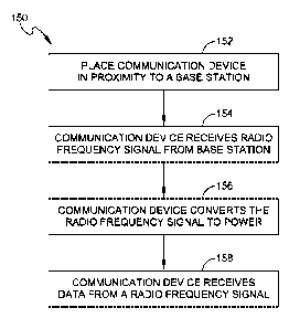
FIG. 2 is a flow chart of a method of operation 150 of a wireless
communication
device according to one embodiment. At block 152, a wireless communication
device,
such as wireless communication devices 104a-104d of FIG. 1, is placed in
proximity to a
base station. At block 154, the wireless communication device receives an RF
signal
from the base station. At block 156, the wireless communication device
converts the RF
signal to a DC voltage to power components of the wireless communication
device. At
block 158, the wireless communication device receives data from the RF signal
from the
base station.
At block 152, the wireless communication device is close enough to the base
station such that the strength of the RF signal emitted by the base station is
sufficient to
power the wireless communication device and, depending on the functionality of
the
particular communication device, it can begin receiving data from or sending
data to the
base station. According to one example, the wireless communication device may
be
between about two feet and about sixty feet from the base station. In other
examples, the
distance between the wireless communication device and the base station is
between
CA 02836588 2013-11-18
WO 2012/166774
PCT/US2012/039951
about one inch and five feet, between about one foot and about ten feet,
between about
two feet and about ten feet, between about two feet and about twenty feet,
between about
five feet and about twenty feet, and between about five feet and about thirty
feet. In other
embodiments, depending on the RF communication technology used, other
distances are
possible.
As described above, at block 154, the wireless communication device receives
an
RF signal from the base station. In one example, the base station is
continuously emitting
an RF signal, and when the wireless communication device enters an area
sufficiently
proximate to the base station, it begins receiving the RF signal.
At block 156, the wireless communication device converts the RF signal to at
least one DC voltage. In one embodiment, after the wireless communication
device has
received sufficient energy to power up, it may also begin to receive data from
the RF
signal, at block 158. The RF signal comprising the data may have a different
source than
the RF signal providing the power, or it may be transmitted from the same base
station.
According to one feature, the wireless communication device is operating in an
area
including multiple base stations, and RF signals from multiple base stations
provide
power to the wireless communication device. The wireless communication device
may
reply to the data-transmitting base station using backscatter modulation. In
one
embodiment, the base station emitting the RF signal that powers the wireless
communication device is also the data-transmitting base station, and it
includes a
transmitter and a receiver that operate simultaneously with data communication
occurring
in one direction at a given time.
16
CA 02836588 2013-11-18
WO 2012/166774
PCT/US2012/039951
According to one embodiment, the RF signal is transmitted at a frequency
between about 840 MHz and about 960 MHz. In another embodiment, the RF signal
is
transmitted at ISM-band frequencies, between about 2.403 GHz and about 2.483
GHz
(used for WiFi). In a further embodiment, the RF signal is transmitted at five
GHz U-Nil
band frequencies, between about 4915 MHz and about 5825 MHz (used for WiFi).
According to another embodiment, the RF signal is transmitted at UMTS/LTE band
frequencies, which may be about 800 MHz, about 850 MHz, about 900 MHz, about
1500
MHz, about 1700 MHz, about 1800 MHz, about 1900 MHz, or about 2100 MHz.
FIG. 3 is a block diagram 200 showing several components of a wireless
communication device according to one embodiment of the invention. The
components
include an analog RF interface 202, a digital control block 204 and a sensor
block 206.
The analog RF interface 202 includes antenna pads 210a and 210b, a voltage
regulator 212, a rectifier 214, a demodulator 216 and a modulator 218. It may
also
include a voltage input 220a if an additional source of DC power, such as a
battery, is
included in the wireless device.
The digital control block 204 includes a voltage input 222 from the analog RF
interface 202, and it may also include a voltage input 220b if an additional
source of DC
power, such as a battery, is included in the wireless device. In various
embodiments, the
digital control block 204 may include anticollision technology, read/write
control, access
control, sensor interface control and a RF interface control. In one example,
the digital
control block 204 includes a finite state machine. In another example, the
digital control
block 204 includes a processor. In other embodiments, the digital control
block may
include a number of logic circuits and processors configured and/or programmed
to
17
CA 02836588 2013-11-18
WO 2012/166774
PCT/US2012/039951
perform functions described herein. According to one feature, the digital
control block
204 converts a digital data packet received from the base station into an
analog signal.
According to another feature, the digital control block 204 converts an analog
signal into
a digital data packet for transmission to the base station.
The sensor block 206 includes an audio output section 230 and an audio input
section 250. In other embodiments, the sensor block 206 may not include both
an audio
output section 230 and an audio input section 250. In other embodiments, the
sensor
block 206 may include one or more of a camera section 240, a video game
controller
section, and a texting interface. The sensor block 206 may also include a
voltage input
220c if an additional source of DC power, such as a battery, is included in
the wireless
device.
The audio output section 230 includes a digital-to-analog converter 232, a
voltage
and current transformation module 234, and an audio output device 236. The
audio
output section is described in greater detail with respect to FIG. 4. In other
embodiments,
components of the audio output section 230 may be located in other functional
blocks.
The audio input section 250 includes an audio input device 260, a voltage and
current transformation module 254, and an analog-to-digital converter (ADC)
252.
According to one embodiment, the sample-and-hold circuit 254 is integrated
into the
ADC 252. According to another embodiment, the audio input section 250 does not
include a sample-and-hold circuit 254. The audio input section 250 is
described in
greater detail with respect to FIG. 6. In other embodiments, components of the
audio
output section 230 may be located in other functional blocks.
18
CA 02836588 2013-11-18
WO 2012/166774
PCT/US2012/039951
According to one aspect, the sensor block 206 receives digital data from the
digital control block 204. For example, the sensor block 206 may receive
digital audio
output data from the digital control block 204. According to one embodiment,
the sensor
block 206 sends digital data to the digital control block 204. For example,
the sensor
block 206 may send digitized audio input data to the digital control block
204. In another
example, the sensor block 206 sends digitized optical data such as a digital
photograph to
the digital control block 204.
According to one embodiment, the sensor block 206 receives digital audio
output
data in a compressed format and decodes it using a local state machine or
processor. The
digital control block 204 may receive digitized audio input and compress or
encode the
data using a state machine or processor. The RF protocol may have specific
commands
or state machine operations to allow the passing of compressed or uncompressed
data.
Various examples of an encoding/decoding algorithms include the LPC (Linear
Predictive Coding), CELP (Code Excited Linear Prediction), SADVQ (Serial
Adaptive
Differential Vector Quantization), ACELP (Algebraic Code Excited Linear
Prediction)
and compressed sensing techniques. Other algorithms may also be used.
According to one feature, the analog RF interface 202 provides a DC voltage
222
to the digital control block 204 to power the components of the digital
control block 204.
According to some embodiments, the analog RF interface 202 sends data received
from
the base station to the digital control block 204.
According to another feature, the digital control block 204 sends data from
the
sensor block 206 to the analog RF interface 202. In various examples, the data
may
19
CA 02836588 2013-11-18
WO 2012/166774
PCT/US2012/039951
represent audio input data from a microphone 260, optical data from a camera
244 and
text input from a keyboard or keypad.
According to one aspect, the analog RF interface 202, the digital control
block
204 and the sensor block 206 are designed to use a minimal amount of power.
For
example, the digital control block 204 in one embodiment includes a finite
state machine
that draws minimal power. Similarly, the components of the sensor block 206
are
designed to minimize power usage. A typical analog RF interface 202 and
digital control
block 204 uses about ten ,uW of power or less.
FIG. 4 is a schematic diagram of one embodiment of the audio output section
230.
The audio output section 230 includes a digital-to-analog converter (DAC) 272,
an
impedance matcher 278, a transformer 274 and earphones 276. The DAC 272 is
connected to the impedance matcher 278 such that the output of the DAC 232 is
input to
the impedance matcher 278. The impedance matcher 278 is connected to the
transformer
274 such that the output of the impedance matcher 278 is input to the
transformer 274.
The DAC 272, the impedance matcher 278 and the transformer 274 are designed to
consume minimal power in transmitting the audio output signal to the earphones
276 by
transforming the high voltage required for complementary metal oxide
semiconductors
(CMOS) or sub-threshold CMOS to the low voltage requirements of a magnetically-
driven earphone.
In one embodiment, the DAC 272 includes a pulse width modulator, low-pass or
band-pass low-loss filter, a voltage input 280 and a digital control 282.
According to one
feature, the DAC 272 including a pulse width modulator has a clock frequency
equal to at
least about twice the Nyquist frequency. When the clock frequency is greater
than about
CA 02836588 2013-11-18
WO 2012/166774
PCT/US2012/039951
twice the Nyquist frequency, there is an oversampling factor to describe the
pulses. In
one example, a 8 kHz audio signal with 8-bits of timing resolution would have
a
sampling rate of 2.048 megasamples per second MSPS (Fs*2^N). The LC tank
circuit or
higher order filter would be tuned to about 8 kHz. The filter may be a low-
pass or band-
pass filter.
In another embodiment, the DAC 272 includes a delta-sigma modulator and a
low-pass or band-pass low-loss filter. According to one feature, the DAC 272
includes a
delta-sigma modulator, and the oversampling ratio is the square root of the
dynamic
range in bits. In one example, an 8-bit kilosamples per second (kSPS) sigma-
delta DAC
would use 64 kSPS 1-bit samples and a first, second or third order low-pass
filter tuned to
about 8 kHz. In some embodiments, the delta-sigma modulator may be first-
order,
second-order or third-order. In one embodiment, the low-loss low-pass filter
may be
implemented with a single-pole inductor-capacitor pair. In another embodiment,
the
inductor may be one leg of the transformer.
In other examples, the DAC 272 can be another low power digital-to-analog
converter. In one example, the DAC 272 has a maximum current between about 5.7
nA
and about 180 nA at a maximum operating voltage of about 0.7 V. The audio
power to
power earphones or headphones, like headphones 276, may be defined using
Equation 1.
SPL conversation SP/ headphone
'audio inaW = 10 10 (1)
where Paudio is the audio power, SPL conversion is the sound pressure level of
the
conversation, and SPLheadphone is the SPL generated from 1 mW of power. In one
example, SPLheadphone is 124 dB SPL/mW, and thus the headphones would use 1
[LW to
21
CA 02836588 2013-11-18
WO 2012/166774
PCT/US2012/039951
generate 94 dB SPL. The voltage of the headphones may be determined using
Equation
(2).
V
headphone AlPauthoRheadph (2)one
where Veadphone is the maximum voltage of the headphones and Rheadphone is the
h
resistance of the headphones. The turns ratio for the transformer 234, in one
embodiment, may be determined using Equation (3).
D2AV
Nturn ¨ max (3)
s V
headphone
where Nturns is the ratio of the number of turns of the primary coil of the
inductor
to the number of turns in the secondary coil of the inductor, and D2AVmax is
the
maximum voltage of the DAC 272. The current at the DAC 272, in one embodiment,
may be determined using Equation (4).
V
D2AI ¨ headphone
(4)
max R IV
headphone turns
where D2A/max is the current of the DAC 272. Note that these equations assume
the transformer is 100% efficient. In other embodiments, D2AV. and D2AImax may
be
higher than would be calculated from these equations.
According to another example, the DAC 272 includes a buck converter or a step-
down DC-to-DC converter using pulse-width modulation. In this example, energy
is
stored in an inductor, allowing the majority of the energy from the source
digital
electronics to be transferred to the audio generating earphones 236,
increasing the
efficiency of the system.
22
CA 02836588 2013-11-18
WO 2012/166774
PCT/US2012/039951
According to one implementation, the DAC 272 includes an additional capacitor,
which is charged to a selected level and then discharged into a comparator.
The
comparator determines the timing of the voltage pulses and permits a higher
pulse width
modulation switching frequency. In one example, the DAC 272 uses sigma-delta
modulation with a switching frequency of 8 kHz and an oversampling ratio of
32. In
another example, the DAC uses sigma-delta modulation with a switching
frequency of
256 kHz at one-bit.
The transformer 274 is an impedance transformer. The impedance transformer
274 converts the analog signal received from the DAC 272 to a lower voltage,
higher
current signal. In various examples, the transformer 274 has a turns ratio of
about 410:1,
about 840:1, or between about 410:1 and about 840:1. The specific design of
the
transformer 274 is selected based on characteristics of the earphones and
provides an
output impedance matched with the input impedance of the earphones.
One embodiment of the transformer 274 is an off-the shelf, miniaturized
transformer with a ferrite magnetic core. According to one feature, a
miniaturized
transformer with a ferrite magnetic core is highly efficient. In another
embodiment, the
transformer 274 is fabricated using semiconductor fabrication techniques with
a planar
magnetic material on the substrate and an etched multi-layer coil providing a
large
number of turns on the DAC side. The number of turns on the DAC side may be,
for
example, about 400, about 500, about 600, about 700, about 800, about 850, or
about
900. A mutli-layer coil on the other side provides a smaller number of turns
(for
example, one, two or more) on the electrical-to-sound pressure device
(earphone).
23
CA 02836588 2013-11-18
WO 2012/166774
PCT/US2012/039951
In one embodiment of the semiconductor transformer 274, there are multiple
arms
feeding the transformer 274, each with a CMOS switch. The CMOS switch may be
used
to switch in a selected number of turns on the DAC side. According to one
feature, the
CMOS switch may be used to maximize efficiency to the fixed impedance of the
earphones. In one embodiment, the turns ratio could be determined upon power-
up and
the switch configuration is stored in non-volatile memory. In another
embodiment, the
switch configuration is pre-configured.
According to some embodiments, the earphones 276 may include earphones or
other electrical-to-audio transducers, including headphones, a speaker, or
another audio
output device. The power requirements for earphones generally vary between
about 5
nW and about 300 nW for human conversation levels at 1 meter. For example,
Ultimate
Ears 7 Pro earphones use about 8 nW of power, Klipsch X5 earphones use about
32 nW
of power, and Apple in-ear earphones use about 260 nW of power. These
calculations
are based on the power requirements to generate adequate sound pressure
levels.
Pressure is related to impedance and velocity:
p =Z-v (5)
where p is the pressure change from standard air pressure at 20 C, Z is the
characteristic impedance of air at standard temperature and pressure and v is
the root
mean squared velocity of the particles in the air medium. Velocity v is
related to the
pressure p and the sound intensity J in W/m2:
v = J 1 pv (6)
and therefore:
J= p2 I ZJ (7)
24
CA 02836588 2013-11-18
WO 2012/166774
PCT/US2012/039951
Normal conversation at about one meter distance has a sound pressure level
between about 40 dB and about 60 dB SPL. If the sound has to travel through an
ear
canal with an aperture of 0.7x0.7 cm2, then earphones would use about 480 pW
to
produce a sound pressure level of 70 dB (at least ten times normal
conversation sound
pressure level at a one meter distance). In one example, Ultimate Ears 7 Pro
(UE7 Pro)
headphones have a sensitivity of 124 dBSPL per mW of input power and an
impedance
of 17.5 ,S2 at 1 kHz. Thus, these headphones use 4.0 nW of power to operate
per channel
and produce a voltage of 260 ,uV rms. Furthermore, according to equations (1)-
(4), for
Ultimate Ears 7 Pro headphones, the primary winding of the transformer would
have
2652 turns and the 0.7V DAC 272 would have a maximum current of 5.68 nA. In
another example, the Apple in-ear headphones, such model MA850G/B have a
sensitivity
of 109 dBSPL/mW and an impedance of 23 ,S2 at 1 kHz. Thus, these headphones
use 130
nW per channel and produce a voltage of 1.70 mV rms. Furthermore, according to
equations (1)-(4), for the Apple in-ear headphones, the primary winding of the
transformer would have 411 turns, and the 0.7V DAC 272 would have a maximum
current of 180 nA.
FIG. 5 is a flow chart of a method of powering an audio output device,
according
to an embodiment of the invention. In one example, the audio output device is
the
earphones 276 of FIG. 4. In block 302, the analog RF interface of a wireless
communication device receives an RF signal from a base station. The analog RF
interface may be the interface 202 of FIG. 3. The analog RF interface
demodulates the
RF signal to produce an input data signal, and sends the input data signal to
the digital
control block 204. At block 304, the digital control block optionally
processes the signal,
CA 02836588 2013-11-18
WO 2012/166774
PCT/US2012/039951
for example by decoding the data from a compressed representation. At block
306, a
digital-to-analog converter converts the digital signal to an analog signal.
The digital-to-
analog converter may be the DAC 272 described with respect to FIG. 4.
According to
one embodiment, the analog signal has a dynamic voltage range that varies from
about
zero volts up to a CMOS logic or sub-threshold logic level. In various
embodiments, the
voltage may be about 0.7 V, about 1.8 V, or between about 0.7 V and about 1.8
V. At
block 308, a transformer converts the analog signal to a lower voltage analog
signal
having a higher current. According to one feature, the transformer converts
the signal
with minimal power loss. Power loss is typically 10-20 percent for
conventional, large
transformers, making them eighty to ninety percent efficient. According to
various
examples, the transformer is about ninety-nine percent efficient, about ninety-
five percent
efficient, about ninety percent efficient, about eighty percent efficient, or
between about
ninety and about ninety-nine percent efficient. The transformer may be the
transformer
274 described with respect to FIG. 4. At block 310, the low voltage analog
signal is
output to an audio output device. At block 312, the output electrical signal
is converted
to sound pressure.
In one embodiment, the received signal provides power to the wireless
communication device and includes data. In another embodiment, the received
signal is a
packet designed specifically for transmitting audio data over the channel. In
another
embodiment, the received signal provides power to the wireless communication
device,
and a different signal provides the data.
FIG. 6 is a schematic diagram of the audio input section 250 and includes a
microphone 290, a buffer 298, a transformer 296, a sample-and-hold circuit
294, and an
26
CA 02836588 2013-11-18
WO 2012/166774
PCT/US2012/039951
analog-to-digital converter (ADC) 292, according to an embodiment of the
invention.
According to one embodiment, the audio input section 250 may also include a
variable
gain amplifier, for example connected to the buffer 298 and the transformer
296.
According to one embodiment, the sample-and-hold circuit 294 is part of the
ADC 292,
and in another embodiment, the audio input section 250 does not include a
sample-and-
hold circuit 294. In another embodiment, the buffer 298 may be a low-noise
amplifier.
In one example, the transformer 296 is an impedance transformer and amplifies
the
voltage by decreasing the current. In another embodiment, the audio output
section 250
does not include a buffer 298, and the buffer 298 functions are implemented in
the
transformer 296. In one example, the transformer is a semiconductor
transformer, such
as the transformer 370 shown in FIG. 8A or the transformer 390 shown in FIGS.
8B and
8C. In one embodiment, the transformer is the transformer 274 used in the
audio output
section 230. In one example, a single transformer, such as the transformer 370
shown in
FIG. 8A, is used for both the audio output device 230 and the audio input
device 250, and
one or more switches can be used to repeatedly adjust the turns ratio of the
transformer as
appropriate for each device.
The analog-to-digital converter 292 has an output signal 262. The microphone
290, buffer 298, variable gain amplifier 296, sample-and-hold circuit 294 and
analog-to-
digital converter 292 are elements of a wireless communication device and are
designed
to consume minimal power in transmitting the audio input signal from the
microphone
290 to the digital control block of the wireless communication device.
The microphone 290 includes an audio transducer that converts sound pressure
differences into electrical energy. In one example, the microphone 290 is an
electret
27
CA 02836588 2013-11-18
WO 2012/166774
PCT/US2012/039951
microphone, and it may be an electret MEMS microphone. In another example, the
microphone 290 is a dynamic microphone. According to one feature, the
microphone
290 operates with a zero Volt bias. The power usage of the microphone may be
between
about 10 pW and about 200pW, and may be calculated using Equations 8 -11. In
particular, the power in a pressure field may be defined using Equation 8.
P = Ap2 I Z (8)
where p is the pressure, Z is the acoustic impedance of air, and A is the area
of
the aperture of the microphone. The acoustic impedance of air Z may be defined
using
Equation 9.
Z = p. c (9)
where p is the density of the medium (here, air), and c is the speed of sound.
According to one example, for air at a temperature of 20 C, the density of air
is 1.184
kg/m3, the speed of sound is 346.1 m/s, and the impedance Z is about 409.8 Pa
s/m.
Note that 60 dB SPL is 2Ø 10-3Pascal at a distance (ri) of 1 m. In one
example, the
distance between the microphone and the mouth (r2) is only about 1/3 meter, so
the SPL
of the transmitted signal is greater. In particular, the pressure is increased
by the ratio
ri/r2. The Power may also be defined for the capacitive sensor using equation
10.
P =-1CV2 f (10)
2
where C is capacitance, V is voltage, and f is frequency. Equation 10 may be
used calculate a voltage to pressure ratio, assuming all the sound power that
enters the
aperture is converted to electrical energy as shown in Equation 11.
dV I dp ¨ f
112A
(11)
ZC
28
CA 02836588 2013-11-18
WO 2012/166774
PCT/US2012/039951
According to one example, the microphone is a Caltech MEMS microphone, as
described by T.Y. Hsu, W.H. Hsieh, Y.-C. Tai and K. Furutani in "A Thin Film
Teflon
Electret Technology for Microphone Applications," A Solid State Sensor,
Actuator and
Microsystems Workshop, Hilton Head, 1996, pp. 235-238
(http://www.audiocircuit.com/A-PDF/AA-Materials-MAT/Membranes-ME/941-DUP-
Teflon-elect-A-A01.pdf). The area A of the aperture of the microphone is 12 x
10-6 m2
(3.5mm per side). Using equations 8-11, if the input frequency f is 250 Hz,
the
microphone is estimated to use about 13 pW of power.
In another example, the microphone is a Briiel and Kjxr 4953 electret
microphone. The area A of the aperture of the microphone is 127 x 10-6 m2
(1/2"
diameter). Using equations 8-11, if the input frequency f is 250 Hz, the
microphone is
estimated to use about 140 pW of power.
According to one embodiment, the peak voltages produced by the microphone are
between about 900 V and about 1.0 mV.
The signal from the microphone 290 is sent to the low noise amplifier 298. The
low noise amplifier 298 amplifies the signal and transmits it to the
transformer 296.
According to one embodiment, the buffer 298 is a low-noise transimpedance
amplifier
operating complementary metal-oxide semiconductor (CMOS) voltage levels. The
CMOS voltage levels may be about 0.7 V, about 1.8 V, or between about 0.7 V
and about
1.8V.
In one embodiment, a variable gain amplifier may be used to amplify the
amplitude of the signal, and output it to an analog-to-digital converter 292.
In one
embodiment, the analog-to-digital converter is the sample-and-hold circuit
294, followed
29
CA 02836588 2013-11-18
WO 2012/166774
PCT/US2012/039951
by an integrating ADC 292. In another embodiment, the analog-to-digital
converter 292
may be a pulse-density converter, such as a sigma-delta analog-to-digital
converter. In
another embodiment, the analog-to-digital converter 292 may be a delta-encoded
ADC.
In another embodiment, the analog-to-digital converter 292 is a success-
approximation
ADC. The sample-and-hold circuit 294 samples the voltage of the signal and
holds it at a
constant level for a period of time. The period of time may be between about
100ns and
about 100 s, and it may be about 100 ns, about 250 ns, about 500 ns, about
750 ns,
about 1 s, about 10 s, about 25 s, about 50 s, about 75 s or about 100 s.
The
sample-and-hold circuit 294 outputs the signal to the ADC 292.
According to one example, the buffer 298, transformer 296 and analog to
digital
converter 292 use about 247 nanowatts of power, based on an 110/step metric.
According to other examples, the buffer 298 and a variable gain amplifier use
about 337
nW of power or about 584 nW of power. In other examples, the power usage of
the
buffer 298 and a variable gain amplifier is about 200 nW, about 250 nW, about
300 nW,
about 350 nW, about 400 nW, about 450 nW, about 500 nW, about 550 nW, about
600
nW, about 750 nW or about 1000 nW.
According to one embodiment, the signal input to the ADC 292 has a voltage
between about 90 V and about 1.0 mV, and the front-end gain of the ADC 292 is
about
40 dB or greater than about 40 dB. In one embodiment, the ADC 292 uses a
switch-
capacitor direct-conversion binary search array. According to one feature,
this minimizes
power consumption by the ADC 292. In one example, the ADC 292 is a successive-
approximation ADC, and it may be a 450 nW, 12-bit, lkS/s SAR ADC which uses
about
3.6 ,uW of power to capture voice up to 8kS/s. In another example, the ADC 292
is a 7.5-
CA 02836588 2013-11-18
WO 2012/166774
PCT/US2012/039951
bit ENOB (effective number of bits) 7.751uW design, with a signal-to-noise
dynamic
range of about 46.92 dB. This design may be implemented in a 0.18 ,um CMOS
(complementary metal oxide semiconductor), which runs at about 500 kS/s, and
has a
Figure of Merit (FOM) of 86 0/conversion step.
FIG. 7 is a flow chart of a method 350 of receiving audio input according to
an
embodiment of the invention. At block 352, audio input is received, for
example by a
microphone. The audio input may be sound pressure differences. At block 354,
sound
pressure differences are converted into electrical energy. Optionally, at
block 356, the
signal may be buffered to produce voltage and current. Optionally, at block
358, the
incoming signal may be converted to a signal with a higher voltage and a lower
current.
In one embodiment, the amplitude of the signal may also be amplified, for
example by a
variable gain amplifier. According to one embodiment, an impedance-
transformation
circuit converts current and voltage (at block 356) and amplifies the
amplitude of the
voltage signal. At block 360, the voltage of the signal is optionally sampled
and held for
a period of time. At block 362, the analog signal is converted to a digital
signal.
According to one embodiment, the conversion of the analog signal to a digital
signal at
block 362 includes sampling the voltage of the signal and holding it for a
period of time.
The digital signal is output to the digital control block of a wireless
communication
device. Optionally, at block 364, the output signal is processed by a
processor. At block
366, the output signal is sent out to a backscatter transceiver, which may be,
for example,
the base station or another RF receiver.
FIG. 8A is a schematic diagram of a transformer 370, including a primary
winding 372, a secondary winding 374, a switch module 376, and a core 378,
according
31
CA 02836588 2013-11-18
WO 2012/166774
PCT/US2012/039951
to an embodiment of the invention. According to one feature, the transformer
370 is a
microfabricated transformer, and the substrate for the fabrication may be
silicon or
another selected material suitable for microfabrication. The primary winding
372 and the
secondary winding 374 are wrapped around the core 378. The primary winding 372
has a
primary current 384. The primary current 384 travels through the switch module
376 and
through the primary winding 372. The secondary winding 374 has a secondary
current
386.
According to one feature, the current 384 passing through the primary winding
372 creates a magnetic field and a changing magnetic field induces a voltage
380 across
the ends of the primary winding 372. The current 386 passing through the
secondary
winding 374 induces a voltage 388 across the ends of the secondary winding
374.
According to one feature, the voltage 380 across the primary winding 372 is
greater than
the voltage 388 across the secondary winding 386.
The switch module 376 is connected to the primary winding 372, and may include
one or more switches 382a-382i. The switch module 376 may be used to adjust
the
number of turns in the primary winding 372. In one example, when the left-most
switch
382a of the switch module 376 is closed, the primary winding 372 has 840
turns. In
another example, when only the right-most switch 382i is closed, the primary
winding
372 has 410 turns. In typical embodiments, only one of the switches 382a-382i
is closed
at a time. According to one embodiment, the switch 376 is an SP9T switch.
According to one feature, the core 378 is constructed of a magnetic material.
For
example, the core 378 may be a ferromagnetic alloy on a silicon surface. In
another
example, the core 378 may be a CoZrRe alloy, such as that described by Mino et
al. in "A
32
CA 02836588 2013-11-18
WO 2012/166774
PCT/US2012/039951
new planar microtransformer for use in microswitching converters." Magnetics,
IEEE
Transactions, vol. 28(4) pp. 1969-73 (2002).
FIG 8B is a side perspective view of a transformer 390 including a primary
winding 392, a secondary winding 394 and a core 398, according to an
embodiment of
the invention. The primary winding 392 and the secondary winding 394 are
wrapped
around the core 398. FIG. 8C is an exploded view of the core 398 of the
transformer 390
showing part of the primary winding 392, according to an embodiment of the
invention.
In one example, the primary winding 392 has 840 turns and the secondary
winding 394
has one turn. In another example, the primary winding 392 has 410 turns and
the
secondary winding 394 has one turn. According to one feature, the core 378 is
constructed on silicon and made with a ferromagnetic alloy.
FIG. 9 is a schematic diagram of a base station 400 that may be used in
conjunction with the wireless communication devices discussed above. The base
station
400 includes a receiver, modem and microprocessor 402, a demodulator 404, a
power
detector 406, a microprocessor 408, a coupler 410, a switch 412, antenna ports
414a-
414c, and a digital control block 416. The diagram shows the path of a
backscattered
signal 420 from one or more wireless communication devices to the receiver
402. When
the base station 400 is turned on, it powers wireless communication devices
within its
range. The power detector 406 is connected to the microprocessor 408, and
monitors the
RF power into the receiver level at the base station. In another embodiment,
another
power detector monitors the RF power level of the transmitted signal.
The coupler 410 is used to couple the transmitter and the receiver of the base
station 400 to the antenna ports through the switch 412 under control of the
digital
33
CA 02836588 2013-11-18
WO 2012/166774
PCT/US2012/039951
control block. The coupler provides the backscatter RF signal to the receiver,
which
includes a demodulator 404, which demodulates the input RF signal to remove
data from
the signal. The transmitter includes an analog baseband signal, which may come
from a
digital to analog converter and low pass filter, and a modulator (I&Q mixer)
that creates
an AM-modulated RF signal to be directed to a wireless communication device
via an
antenna.
FIG. 10 is a block diagram of a wireless communication device 450 including an
RF transceiver 452 and an audio output device 454, according to an embodiment
of the
invention. The communication device 450 may also include an audio input device
456, a
camera 458, a processor 464, memory 466, a battery 460 and a user interface
462. The
user interface may include a keyboard and display. The wireless communication
device
also includes a processing section. According to one feature, the wireless
communication
device 450 is passively powered by an RF signal. For example, the RF signal
may
passively power the RF transceiver 452 and one or more of the audio output
device 454,
the audio input device 456 and the camera 458.
In one embodiment, the wireless communication device 450 is a dual mode
wireless communication device, such as a cellular telephone or a smart phone,
and
includes a battery 460. In a first mode, the wireless communication device 450
operates
passively using an RF signal and does not draw DC power from the battery 460.
The
functionality of the wireless communication device 450 is limited in the first
mode, and
in one embodiment in the first mode, the dual mode wireless communications
device
communicates with a base station and can continue to receive messages, for
example
email messages, web content, text messages and phone calls without drawing
power from
34
CA 02836588 2013-11-18
WO 2012/166774
PCT/US2012/039951
the battery. In a second mode, the wireless communication device 450 draws
power from
the battery, and can perform all the functions of a typical wireless
communication device
of its kind.
In another embodiment, in a first mode, the wireless communication device 450
operates using an RF signal and draws minimal DC power from the battery 460.
This
may be considered a battery-assisted passive mode. The functionality of the
wireless
communication device 450 is limited in the first mode, and in one embodiment
in the first
mode, the dual mode wireless communications device communicates with a base
station
and can continue to receive messages, for example email messages, web content,
text
messages and phone calls without drawing power from the battery. In a second
mode,
the wireless communication device 450 draws power from the battery, and can
perform
all the functions of a typical wireless communication device of its kind.
According to one embodiment, the wireless communication device is a mobile
phone, and the RF signal provides an indication to the mobile phone that it is
receiving an
incoming call. The receipt of the indication that the mobile phone is
receiving an
incoming call wakes up the mobile phone and it can receive the call.
FIG. 11 is a flow chart of a method 500 of sending and receiving data in a
dual
mode wireless communication device according to an embodiment of the
invention. The
method 500 includes a backscatter method 502 that can be performed without
drawing
power from a battery. The backscatter method 502 may also be performed using
some
battery power but significantly less battery power than current communication
devices.
At block 504, the wireless communication device determines whether there is a
backscatter connection available by searching for an RF signal. If no
backscatter
CA 02836588 2013-11-18
WO 2012/166774
PCT/US2012/039951
connection is available, the wireless communication device operates in its
battery-
powered mode using another connection, such as a WiFi, 3G, 4G or other
WLAN\WAN
connection. If a backscatter connection is available, at block 506 the
wireless
communication device establishes a connection with the base station and
determines if
there is data available. In one example, the data represents one or more email
messages.
The data may be available to download from a server, or to upload from the
wireless
communication device to a server. In various embodiments, the data may be sent
by
modifying a protocol, such as TCP/IP (Transmission Control Protocol/Internet
Protocol)
or UDP/IP (User Datagram Protocol/Internet Protocol). In another embodiment,
the data
is sent directly over the wireless channel as packetized data, for example,
SMTP (Simple
Mail Transfer Protocol), HTML (Hyper Text Markup Language), SMS (Short Message
Service), IM (Instant Messaging), phone call information, or voice-mail.
At block 508, the wireless communication device receives or sends data,
thereby
filling or emptying a first-in first out (FIFO) queue. According to one
implementation, at
block 510, the wireless communication device determines if the FIFO receiving
data is
full. If the FIFO receiving data is full, at block 518 the wireless
communication device
wakes up the processor to empty the FIFO. If the FIFO receiving data is not
full, at block
512 the wireless communication device determines if the data transfer is
complete. If the
data transfer is not complete, the method returns to block 508 and receives
more data.
According to one example, the amount of data in the FIFO is the fill state of
the FIFO. In
this example, if the FIFO is empty, the fill state indicates that the FIFO is
empty, and if
the FIFO is full, the fill state indicates that the FIFO is full. In one
example, the fill state
indicates the amount or percentage of space remaining in the FIFO.
36
CA 02836588 2013-11-18
WO 2012/166774
PCT/US2012/039951
In another implementation, at block 510, the wireless communication device
determines if the FIFO sending data is empty. If the FIFO sending data is
empty, at block
518 the wireless communication device wakes up the processor to fill the FIFO.
If the
FIFO receiving data is not empty, at block 512 the wireless communication
device
determines if the data transfer is complete. If the data transfer is not
complete, the
method returns to block 508 and sends more data. The FIFO may be used in the
fully
passive audio mode or it may be used for other types of data. According to one
embodiment, the fully passive audio mode functions without a FIFO.
According to one feature, the method 500 preserves battery power in a dual
mode
wireless communication device by using the backscatter method 502 when
available.
The wireless communication device can be in a sleep mode and continue to
receive
messages while performing the method 502 without drawing any power from the
battery,
greatly extending the life of the battery.
In embodiments described above, wireless communications devices communicate
with a local base station. In one implementation, a facility may include a
number of base
stations distributed throughout the facility and a user of a wireless device
may move
through the facility connecting to different base stations based on the user's
locations.
The base stations may communicate with each other using wired or wireless
technologies
such as WiFi, 3G and 4G, to coordinate communications with each of multiple
wireless
communications devices. Also, each base station may operate with more than one
wireless communications device.
37
CA 02836588 2013-11-18
WO 2012/166774
PCT/US2012/039951
As discussed above, embodiments of the present invention provide significant
advantages in wireless communications devices by allowing the devices to
operate
without battery power completely or in certain modes of operation.
Having thus described several aspects of at least one embodiment, it is to be
appreciated various alterations, modifications, and improvements will readily
occur to
those skilled in the art. Such alterations, modifications, and improvements
are intended
to be part of this disclosure and are intended to be within the scope of the
invention.
Accordingly, the foregoing description and drawings are by way of example
only, and the
scope of the invention should be determined from proper construction of the
appended
claims, and their equivalents.
What is claimed is:
38