Note: Descriptions are shown in the official language in which they were submitted.
CA 02836609 2013-11-19
WO 2012/160005
PCT/EP2012/059308
SCANNING DEVICE FOR LOW COHERENCE INTERFEROMETRY
Field
Embodiments of the invention relate to the fields of high-resolution optical
coherence
tomography.
Background
Optical Coherence Tomography (OCT) is a technique for the generation of
medical
images that can provide axial information at a high resolution using a
broadband light source
and an interferometric detection system. It has found a wide range of uses,
from cardiology
to ophthalmology and gynecology, or for in-vitro sectional studies of
biological materials.
Axial information is obtained in OCT through interferometric methods. To
generate
images (2D) and volume representations (3D) of the histology of tissue, it is
necessary to
move the beam laterally over the area of interest. This movement has been
traditionally
done by means of mechanical displacement of some optical element within the
system such
as the waveguide in the case of fiber-based systems. Alternatively, the sample
can be
moved underneath a stationary beam. The most common solution utilizes a moving
mirror in
the beam path in the sample arm of the interferometer. Although this method is
effective, it
has drawbacks, especially in terms of reliability, manufacturing cost,
maintenance cost,
complexity of adjustment, final system size, etc. The use of MOEMS technology
(Micro-opto-
electromechanical systems) has been proposed and demonstrated for situations
in which
conventional mirrors are not acceptable, such as in catheters or laparoscopic
instruments.
However, these devices suffer from many of the same problems as their
macroscopic
versions and they pose their own challenges in terms of encapsulation,
sterilization, etc.
One approach for providing a lateral scan over a sample is to use multiple
beams. An
example of this was proposed in patent application WO 2010/134624. Several
complete
interferometers working in parallel are described that only share the light
source. As such,
the sample arm of every interferometer consists of a single optical path and
there is no
multiplexing mechanism leading to a structurally complicated system.
Another patent application, WO 2004/073501, contemplates the use of multiple
beams that are simultaneously incident on the sample. The aim of this
application is the
combination of these beams in a controlled manner through the use of
modulators and phase
delays. The combined illumination over the sample shows a certain interference
pattern.
Working with the modulators and phase delay elements, the position of the
interference
pattern of the illumination on the sample can be varied and, subsequently, it
is possible to
reconstruct a three dimensional image of the sample using signal processing
techniques.
CA 02836609 2013-11-19
WO 2012/160005
PCT/EP2012/059308
- 2 -
The application does not use multiplexing means to distinguish light collected
from a plurality
of optical paths. There is only a single optical path that collects the light
reflected from the
sample.
In an article by Yamanari et. Al, "Full-range polarization-sensitive swept-
source
optical coherence tomography by simultaneous transverse and spectral
modulation," Optics
Express Vol. 18, Issue 13, pp. 13964-13980, 2010, a polarization sensitive SS-
OCT system
(Swept Source OCT) is described. In this system, and with the aim of solving
the problem of
complex conjugates typical of SS-OCT and FD-OCT systems (Fourier Domain OCT),
phase
modulation is applied to the reference arm. This phase is modified while
electro-mechanical
means scan the sample laterally. This document, therefore, does not describe
the use of
modulation in the sample arm. Moreover, in the case of Time Domain OCT systems
(TD-
OCT), the scanning speed of the variable delay element in the reference arm
can be a
limitation of the final system performance, to the extent that its operating
speed or maximum
scanning range may be insufficient for the application of interest.U.S. Patent
6198540 and
patent application EP 1780530 each describe systems that use multiple optical
paths in the
reference arm. However, each system uses traditional free space optics and
mechanical
means for the lateral scan of the sample.
Brief Summary
Systems and methods for performing low-coherence lateral scanning of a sample
while minimizing (and in some embodiments eliminating) the use of mechanical
elements is
presented. In an embodiment, the system divides a sample arm into several
optical paths
and uses a plurality of outputs that send and receive beams to and from
different areas of a
sample, thus retaining the ability to differentiate at any time the light
received from reflections
at different depths within the sample.
According to an embodiment, a low coherence interferometry system includes a
first
multiplexing unit and a second multiplexing unit. The first multiplexing unit
is configured to
receive a first beam of radiation and includes a first plurality of optical
delay elements. The
first plurality of optical delay elements is configured to introduce a group
delay to the first
beam of radiation based on an optical path traversed by the first beam of
radiation among a
first plurality of optical waveguides. The second multiplexing unit is
configured to receive a
second beam of radiation. In an embodiment, the second beam of radiation is
the same as
the first beam of radiation. In another embodiment, the second beam of
radiation is different
from the first beam of radiation. The second multiplexing unit includes a
second plurality of
optical modulating elements. The second plurality of optical modulating
elements is
configured to differentiate the second beam of radiation among a second
plurality of optical
CA 02836609 2013-11-19
WO 2012/160005
PCT/EP2012/059308
-3 -
waveguides to produce one or more output radiation beams. The second plurality
of optical
waveguides is configured to guide the one or more output radiation beams
towards a
sample.
In an embodiment, a method includes receiving a beam of radiation at a first
multiplexing unit. Then, a group delay is introduced to the beam of radiation
received at the
first multiplexing unit based on an optical path traversed by the beam of
radiation received at
the first multiplexing unit among a first plurality of optical waveguides in
the first multiplexing
unit. A beam of radiation is received at a second multiplexing unit. In an
embodiment, the
beam of radiation received at the second multiplexing unit is the same as the
beam of
radiation received at the first multiplexing unit. In another embodiment, the
beam of radiation
received at the second multiplexing unit is different from the beam of
radiation received at the
first multiplexing unit. The beam of radiation received at the second
multiplexing unit is
differentiated in the second multiplexing unit among a second plurality of
optical waveguides
to produce one or more output radiation beams. The one or more output
radiation beams
are guided towards a sample.
Brief Description of the Drawings/Figures
The accompanying drawings, which are incorporated herein and form a part of
the
specification, illustrate embodiments of the present invention and, together
with the
description, further serve to explain the principles of the invention and to
enable a person
skilled in the pertinent art to make and use the invention.
FIG. 1 illustrates a block diagram of an OCT system, according to an
embodiment.
FIG. 2 illustrates a block diagram of a lateral scanning system, according to
an embodiment
FIG. 3 illustrates an example of a time-division multiplexing unit.
FIGs. 4-6 illustrate examples of first multiplexing units, according to
embodiments.
FIGs. 7-12 illustrate examples of second multiplexing units, according to
embodiments.
FIG. 13 illustrates the use of beam steering elements with the second
multiplexing unit,
according to an embodiment.
FIGs. 14-15 illustrate examples of using one or more optical elements to focus
the light,
according to embodiments.
FIG. 16 illustrates a sample depth scanning technique according to an
embodiment.
FIG. 17 illustrates the use of a gradient index lens with the multiplexing
units, according to an
embodiment.
FIGs. 18A-B illustrate two views of a reflecting optical element with the
multiplexing units,
according to an embodiment.
CA 02836609 2013-11-19
WO 2012/160005
PCT/EP2012/059308
- 4 -
FIGs. 19-20 illustrate the use of adjustable reflecting elements with the
multiplexing units,
according to embodiments.
FIG. 21 illustrates a flowchart of an example method, according to an
embodiment.
Embodiments of the present invention will be described with reference to the
accompanying
drawings.
Detailed Description
Although specific configurations and arrangements are discussed, it should be
understood that this is done for illustrative purposes only. A person skilled
in the pertinent art
will recognize that other configurations and arrangements can be used without
departing
from the spirit and scope of the present invention. It will be apparent to a
person skilled in
the pertinent art that this invention can also be employed in a variety of
other applications.
It is noted that references in the specification to "one embodiment," "an
embodiment,"
"an example embodiment," etc., indicate that the embodiment described may
include a
particular feature, structure, or characteristic, but every embodiment may not
necessarily
include the particular feature, structure, or characteristic. Moreover, such
phrases do not
necessarily refer to the same embodiment. Further, when a particular feature,
structure or
characteristic is described in connection with an embodiment, it would be
within the
knowledge of one skilled in the art to effect such feature, structure or
characteristic in
connection with other embodiments whether or not explicitly described.
Embodiments described herein provide for sample scanning using optical
coherence
tomography (OCT) while avoiding or minimizing the use of mobile mechanical
parts for the
lateral displacement of the beam across the sample. Additionally, embodiments
provide
certain advantages such as an increase in the effectiveness of the axial scan.
Spatial
diversity schemes may be implemented by measuring the same sample region from
different
directions simultaneously, which reduces speckle and other types of noise in
the
measurements. Also, measurements of the scattering of light from the sample in
different
directions can be collected, thereby providing information about sample
scattering anisotropy
and directionality.
In various embodiments, different optical paths for a beam of radiation to
travel are
uniquely distinguished by means of multiplexing techniques that allow for the
separation of
different spatial positions during image processing. Any multiplexing
technique may be
applicable (time domain, frequency, code division, etc.). In one example, time
domain
multiplexing can be advantageously combined with other multiplexing
techniques, such as
frequency multiplexing.
Discussed below is an example OCT system that includes
multiplexing features to produce multiple output paths for the beam of
radiation to travel.
CA 02836609 2013-11-19
WO 2012/160005
PCT/EP2012/059308
-5 -
FIG. 1 illustrates an OCT system 101, utilizing an optical compensating
element 112,
and used for imaging a sample 110, according to an embodiment. For example,
optical
compensating element 112 may compensate for chromatic dispersion or any other
type of
aberration of the light within OCT system 101. In another example,
compensating element
112 may merely reflect back incoming light without applying any particular
modulation to the
light. The use of the term "light" may refer to any range of the
electromagnetic spectrum. In
an embodiment, the term "light" refers to infrared radiation at a wavelength
of about 1.3 pm.
OCT system 101 further includes an optical source 102, a splitting element
104, a sample
arm 106, a reference arm 108, a detector 114, and a scanning system 116. In
the
embodiment shown, compensating element 112 is located within reference arm
108,
however, it should be understood that compensating element 112 may also be
located in
sample arm 106. Alternatively, compensating element 112 may be present in both
sample
arm 106 and reference arm 108. In one example, sample arm 106 and reference
arm 108
are optical waveguides such as patterned waveguides or optical fibers. In an
embodiment,
all of the components of OCT system 101 are integrated onto a planar lightwave
circuit
(PLC). Other implementations may be considered as well, such as, for example,
fiber optic
systems, free-space optical systems, photonic crystal systems, etc.
It should be understood that OCT system 101 may include any number of other
optical elements not shown for the sake of clarity. For example, OCT system
101 may
include mirrors, lenses, gratings, splitters, micromechanical elements, etc.,
along the paths of
sample arm 106 or reference arm 108. OCT system 101 may include various
modulating
elements configured to suppress contributions of interference signals
generated in non-active
optical paths. In another example, OCT system 101 may include MEMS (Micro
Electro
Mechanical Systems), which apply an additional physical lateral scan to the
beams. An
optical element in the path of the light may be displaced by electromechanical
actuators (e.g.
based on thermal expansion, piezoelectric or electrostatic force) that are
integrated by
means of microfabrication techniques.
Splitting element 104 is used to direct light received from optical source 102
to both
sample arm 106 and reference arm 108. Splitting element 104 may be, for
example, a bi-
directional coupler, an optical splitter, or any other modulating optical
device that converts a
single beam of light into two or more beams of light.
Light that travels down sample arm 106 traverses scanning system 116 before
ultimately impinging upon sample 110. Scanning system 116 may include one or
more
multiplexing units, with each unit differentiating the light among a plurality
of optical paths.
For example, scanning system 116 may include one multiplexing unit that
selects an optical
path associated with a particular group delay. The group delay applied to the
light as it
CA 02836609 2016-10-11
6=
travels down the selected path determines a scan depth of the light in sample
110. In
another example, scanning system 116 may include another multiplexing unit
that
differentiates the light among a plurality of output waveguides to produce one
or more output
radiation beams. The output radiation beams may impinge upon sample 110 at
different
regions on sample 110 and may be directed from different directions. More
details regarding
the various multiplexing units are discussed herein.
Sample 110 may be any suitable sample to be imaged, such as tissue. During an
OCT procedure, the light scans at a certain depth within sample 110 and the
scattered
radiation is collected back into sample arm 106. In another embodiment, the
scattered
radiation is collected back into a different waveguide from the transmitting
waveguide.
Light within sample arm 106 and reference arm 108 is recombined before being
received at detector 114. In the embodiment shown, the light is recombined by
splitting
element 104. In another embodiment, the light is recombined at a different
optical coupling
element than splitting element 104.
In an embodiment, using scanning system 116 for various scan depths increases
the
performance of the rest of OCT system 101. Due to the various group delays
applied to the
light in scanning system 116, detected interference signals can be separated
(in time,
frequency, space, code, etc.,) for each scan depth at detector 114. OCT system
101 may be
used with all varieties of scanning systems, including time domain, frequency
domain and
swept source.
In another embodiment, a subset of the output radiation beams is directed
towards
the same area of sample 110, so that measurements for that area are obtained
from different
directions. In this way, angular diversity can be used to reduce noise in the
measurements
as described in "Array detection for speckle reduction in optical coherence
microscopy," J.M.
Schmitt, Phys. Med. Biol. vol. 42, issue 7, 1997.
Since the total distance traveled by each
radiation beam of the subset will be different, the scanning depth may be
independently
controlled for each optical path.
In another embodiment, an angular scattering function of the light from sample
110
may be measured from directions differing from the incident direction, to
provide valuable
information about sample anisotropy. Such measurements are possible due to the
plurality
" of output waveguides in scanning system 116 that can be configured to face
the same region
of sample 110. Additionally, the scanning depth may again be independently
controlled for ,
each optical path to account for any differences in light travel distance.
FIG. 2 illustrates a first multiplexing unit 17 and a second multiplexing unit
9,
according to an embodiment. Each multiplexing unit may be a part of scanning
system 116
CA 02836609 2013-11-19
WO 2012/160005
PCT/EP2012/059308
- 7 -
illustrated in FIG. 1. First multiplexing unit 17 receives a beam of radiation
from a waveguide
7. First multiplexing unit 17 applies a group delay to the beam of radiation
based on a
selected optical path within first multiplexing unit 17. In one example, the
optical path is
chosen based on time division multiplexing. In another example, the light is
differentiated
amongst a plurality of optical paths based on frequency division multiplexing.
"Differentiating," as used herein, may refer to directing light down one or
more specific optical
paths (as may be the case with time division multiplexing, for example).
"Differentiating," as
used herein, may also refer to causing light traversing a given optical path
to be
distinguishable from light traversing other optical paths, even if light is
traversing those
optical paths at the same time (as may be the case with frequency division
multiplexing or
coherence division multiplexing, for example). More detailed examples of first
multiplexing
unit 17 are illustrated in FIGs. 4-7.
Second multiplexing unit 9 receives the beam of radiation from first
multiplexing unit
17. Although only a single waveguide is illustrated connecting the two
multiplexing units, it
should be understood that any number of waveguides may be used to transfer
light between
the two multiplexing units. Second multiplexing unit 9 differentiates the
received beam of
radiation among a plurality of output waveguides 8 to produce one or more
output radiation
beams. In one example, this differentiation is performed via time division
multiplexing. In
another example, the differentiation is performed via frequency division
multiplexing. In
another example, the differentiation is performed via coherence domain
multiplexing. It
should be understood that any combination of the above mentioned techniques
may be
utilized as well to differentiate the beam of radiation among output
waveguides 8. More
detailed examples of second multiplexing unit 9 are illustrated in FIGs. 8-14.
Various embodiments describe at least one form of multiplexing between an
input
waveguide and one or more output waveguides to separate the different spatial
positions at
an image processing time. Any type of multiplexing (time division, frequency,
coherence,
code division, etc.) is applicable. Although embodiments herein may illustrate
both first
multiplexing unit 17 and second multiplexing unit 9 being a part of sample arm
106, it should
be understood that this does not have to be the case. For example, in any of
the preceding
embodiments, first multiplexing unit 17 may be located in reference arm 108
while second
multiplexing unit 9 is located in sample arm 106. In this example, first
multiplexing unit
modulates light in reference arm 108, while second multiplexing unit modulates
light in
sample arm 106.
FIG. 3 illustrates an example of light multiplexing for a relatively small
number of
outputs, but it may be considered analogous for a greater number as well. Each
optical
switch 2 deflects the light of an input waveguide to one of two output
waveguides. Switch 2
CA 02836609 2013-11-19
WO 2012/160005
PCT/EP2012/059308
- 8 -
can be implemented using integrated optical elements, such as Mach-Zehnder
interferometers or 2x2 configurable couplers. Additionally, modulating
elements such as
electro-optic, thermo-optic and acousto-optic modulators may be implemented
for directing
the light between the various waveguides.
In an embodiment, optical switches 2 are
sufficiently broadband to perform efficiently on the entire light spectrum
used in OCT system
101. FIG. 3 also illustrates one of the possible selectable optical paths 10
through the usage
of switches 2.
According to an embodiment, scanning system 116 includes a multiplexing system
for
different ranges of depth scanning. One aim is to reduce the requirements on
the axial
scanning speed or its maximum range, or increase the actual scanning speed
given some
characteristics of the element in reference arm 108 of OCT system 101. High
lateral
scanning speeds can be reached using the multiplexing resources illustrated in
FIG. 3.
FIGs. 4A and 4B illustrate two examples of first multiplexing unit 17, labeled
401 and
402, in the frequency domain for different depth scanning ranges through the
insertion of
delay elements 11. Delay elements 11 cause defined group delays in the light
that passes
through them in the different optical paths 10. Multiplexing units 401 and 402
further include
modulating elements 3 used to differentiate the light, for example, in the
frequency domain,
among the various optical paths through delay elements 11.
The placement of delay elements 11 in multiplexing unit 401 each add a delay
to their
respective portion of the optical path. An optical path having a desired
delay, such as optical
path 10, can then be selected by adding appropriate delays together along the
optical path.
The placement of modulating elements 3 in multiplexing unit 402 modulates a
relative
decrease of added delay in each optical path 10. The goal is to produce a
plurality of
possible optical paths 10, each with a different total group delay. In this
manner, a desired
group delay can be implemented in the OCT system to image different depths
without
moving parts. In an example, each of these optical paths 10 is modulated using
a
characteristic frequency. Delay elements 11 may be implemented in a variety of
ways, such
as by using waveguide segments of different lengths or waveguide segments
allowing
modification of the refractive index by means of some effects such as thermo-
optical, thermo-
electric, charge injection, etc. The frequency modulation may be obtained by
using
modulating elements 3 with a linear behavior in the range [0,27], as it
appears in the
interference signal that is collected at detector 114.
FIGS. 4A-4B show designs based on a sequence of cascaded couplers 5, such as
2x2 couplers, that are characterized by their conservative nature in terms of
optical energy.
Indeed, all the optical power is transmitted down the branching waveguides at
each
cascaded coupler 5 between elements. Despite the similarity of the design with
a cascaded
CA 02836609 2013-11-19
WO 2012/160005
PCT/EP2012/059308
- 9 -
Mach-Zehnder interferometer, there are no interference effects taking place in
the elements,
as all relative introduced delays are much greater than the coherence length
of the source.
In either multiplexing unit 401 or 402, for different scanning depth ranges
shown in
FIGs. 4A-4B, the goal is not to find a complete transformation of depth into
frequency, but a
multiplexing of depth ranges by means of frequency division. The complete
transformation
may cause some of the relative delays to be comparable to, or smaller than,
the coherence
length of the source, in which case interference effects would appear.
The division within the various possible optical paths 10 with different
accumulated group
delays may also be achieved by using, for example, time division multiplexing.
FIG. 5 illustrates another example of first multiplexing unit 17 (labeled 501)
that
includes optical switching elements 2 in a first network 502 and a second
network 504.
Multiplexing unit 501 further includes delay elements 11. In an embodiment,
delay elements
11 are configured to apply different group delays depending on the selected
optical path 10.
In one example, second network 504 of optical switches 2 guides light from any
of the
plurality of possible optical paths through delay elements 11 to a single
waveguide output.
Since optical switches 2 may not be ideal, some light may leak into paths
other than the
intended optical path 10. The noise generated by this leaked light may cause
problems with
the large dynamic range characteristics of the heterodyne detection systems
commonly used
in OCT. In an embodiment, to mitigate the situation regarding the leaked
light, optical
modulators 3 can be inserted on each optical path, such that they can
individually modulate
light on a given path. In one example, the modulation is performed via phase
modulators.
Thus, the light in optical path 10 is shifted in frequency with regard to the
other optical paths,
suppressing possible interferences. It should be understood that if optical
switches 2 have a
sufficiently high switching ratio, then optical modulators 3 may not be
required.
The configuration shown in multiplexing unit 501 allows individual selection
of group
delays for each optical path 10, which can be useful to define different areas
of scanning. In
another embodiment, uniform spacing may be achieved over the scanning range by
using a
simpler design.
For example, another example of first multiplexing unit 17 is illustrated in
in FIGs. 6A-
B (labeled 601). Multiplexing unit 601 is capable of selecting an optical path
10 with a unique
group delay, but with a smaller number of delay elements 11 and optical
switches 2 than the
embodiment shown in FIG. 5. In one embodiment, optical modulators 3 may be
included in
each switchable optical path 10 as illustrated in FIG. 6A. In this way,
selected optical path 10
is modulated, for example, at a unique frequency, so that the light can be
filtered from other
optical paths. Similar to the discussion above in regards to FIG. 5, if the
switching
technology is able to minimize the light that leaks into an undesired path, or
if the
CA 02836609 2013-11-19
WO 2012/160005
PCT/EP2012/059308
- 10 -
interference is discarded from the signals through some other means, then
optical
modulators 3 may be removed. An example multiplexing configuration without
optical
modulators 3 is illustrated in FIG. 6B.
Time multiplexing systems have a possible advantage in terms of optical power
efficiency. Although the use of first multiplexing system 17 for different
ranges of depth
scanning, such as the examples illustrated in FIGs. 4 and 6, is relatively
efficient in terms of
conservation of optical power, half of the optical power is lost at its output
since there are two
output waveguides. In an embodiment, a form of phase modulation is applied to
the two
output branches to allow for their separation in the frequency domain.
Additionally, second
multiplexing unit 9 may be included to receive the output from both branches.
Time division
multiplexing systems do offer an advantage, namely, the flexibility to select
a particular scan
region. For example, it is possible to obtain an image with interlaced depth
ranges, giving
higher priority to certain depth ranges of the image, which would be scanned
more often than
others, or even concentrate scanning time on a subset of all available ranges
during
operation.
In an embodiment, optical switches 2 may be designed to alternate between a
balanced directional optical coupler and a proper switch. Thus, advantages of
multiplexing in
the frequency domain and the time domain could be combined. For example,
optical
switches 2 may be left in a state of balanced directional optical coupler to
make various
depth ranges be illuminated simultaneously, while other switches may be
switched
conventionally for sequential access of a particular optical path.
If optical switches 2 acting as couplers allow the distribution of energy
between their
branches in a controlled and flexible manner (e.g., with a variable division
ratio), then it is
possible to partition the amount of optical power used to sample at each
depth. The power
may be adjusted so as to obtain a uniform signal to noise ratio, or in another
manner optimal
for the specific application. Alternatively, this can be achieved in the time
domain by
adjusting the duration of the depth scan for each configuration of first
multiplexing unit 17, or
accumulating a variable number of lines depending on depth. The various time
multiplexing
embodiments may result in different period fractions being allotted to
configurations of optical
switches 2 belonging in different optical paths 10.
In an embodiment, multiplexing is introduced in some form to the separate
contributions from both output branches of first multiplexing unit 17. For
example, frequency
modulation, time multiplexing, or introducing a differential delay in one of
the branches that is
larger than the scanning range are all multiplexing designs that may be
implemented. In the
last example, it may be necessary that there are no signals with significant
magnitude
CA 02836609 2013-11-19
WO 2012/160005
PCT/EP2012/059308
- 11 -
coming from tissue depths greater than the scanning distance, to avoid
interference between
the branches.
FIG. 7 illustrates an example of second multiplexing unit 9 (labeled 701)
using time
division multiplexing, according to an embodiment. The illustrated system
includes
waveguide 7, output waveguides 8, first multiplexing unit 17 and multiplexing
unit 701. FIG.
7 illustrates one possible combination of any scan range multiplex system with
a time
multiplex system for lines in the lateral direction. This maximizes the use of
available light
power and device signal to noise ratio. In this system, a desired optical path
10 may be
selected using optical switches 2 to direct light to a particular waveguide 8.
The paths may
be sequentially selected, for example, to achieve a scanning functionality
where light is
passed through each waveguide 8 in a sequential manner.
FIG. 8 illustrates an example where the time division multiplexing of second
multiplexing unit 9 has been replaced by a frequency multiplexing unit 801.
Frequency
multiplexing unit 801 includes optical paths 10 associated with the different
lateral scanning
lines, according to an embodiment. Each branch of optical path 10 may have an
associated
optical modulator 3. In one example, a tree of directional couplers is used to
split the
incoming light among all optical paths. Frequency multiplexing unit 801 has a
further
advantage of allowing simultaneous detection of all lateral scanning lines.
However, there
does exist a loss of the light energy collected by each output waveguide 8
when traveling
back through the tree of couplers. Assuming that the directional couplers are
balanced and
ideal, this approach presents excess losses of approximately 3*10g2 (N) dB,
where N is the
number of branches of each tree of couplers, when compared with an equivalent
time
multiplexed system. As a result, a lower signal to noise ratio may be obtained
in the present
embodiment when compared, for example, to the time division multiplexing
embodiment
illustrated in FIG. 7.
In another embodiment, coherence domain multiplexing may be used within second
multiplexing unit 9, which leaves the task of separating lateral lines to the
axial scan of the
interferometric system. FIG. 9 illustrates the use of a coherence domain
multiplexing unit
901 as an example of second multiplexing unit 9 together with first
multiplexing system 17,
according to an embodiment. This method uses trees of directional couplers
with delays on
every branch, such that when light reaches output waveguides 8, the various
optical paths 10
have accumulated a unique delay for every output waveguide 8. In one example,
the
minimum spacing between the accumulated delays associated with the different
output
waveguides 8 is larger than the delay associated with the maximum sample depth
from
which optical contributions are expected.
CA 02836609 2013-11-19
WO 2012/160005
PCT/EP2012/059308
- 12 -
In an embodiment, combinations of any of the previously described multiplexing
techniques may be utilized within second multiplexing unit 9. For example,
frequency
division multiplexing allows for parallel readout, but it is less efficient in
terms of optical power
budget, while time division multiplexing is better at conserving optical
power. FIG. 10
illustrates a multiplexing unit 1001 that combines both optical switches 2 and
optical
modulators 3. In this example, optical switches 2 are placed at the first path
divide while the
optical modulators 3 are used at the various other optical paths formed after
the first path
divide.
As mentioned previously, optical switches 2 may not be ideal. This may lead to
light
leakage down optical paths that are different from the selected optical path
10. This can
cause interference between independent lateral lines. The interference
contribution may be
minor if optical switch 2 has a reasonable performance, because of the
accumulation of non-
active optical path suppression in backward and forward directions. In one
example, optical
modulators 3 may be included before each output waveguide 8, as illustrated in
multiplexing
unit 1101 of FIG. 11. Optical modulators 3 may be phase modulating elements
that apply a
periodic excitation to shift the carrier of the interference pattern
associated with each output
waveguide 8 to a different frequency.
In an embodiment, second multiplexing unit 9 may include independent scan
depth
multiplexing units for each optical path. FIG. 12 illustrates a combination of
time division
multiplexing units 1201 with an additional first multiplexing unit 17 included
on each optical
path. First multiplexing unit 17 may be implemented using one or more of the
examples
illustrated in FIGs. 4-6. In this embodiment, a unique scan depth may be
chosen for each
output waveguide 8, while the various optical paths are all multiplexed during
a lateral scan.
Due to factors such as the complexity of the integrated optical system, or the
minimum spacing between output waveguides 8 necessary to avoid coupling
between them,
it may be possible that an adequate coverage of the lateral space for a scan
cannot be
reached for a given set of design constraints. Thus, in another embodiment,
the beams
produced from each output waveguide 8 may be steered to cover the scanning
space with
sufficient density.
FIG. 13 illustrates an example including first multiplexing unit 17 and second
multiplexing unit 9, where the radiation beams produced from each output
waveguide 8 may
be steered to exit the ends of output waveguides 8 at a specific angle via
beam steering
elements 12. Although a particular example of second multiplexing unit 9 is
shown in FIG.
13, it should be understood that any other embodiment of second multiplexing
unit 9 may be
used as well.
CA 02836609 2013-11-19
WO 2012/160005
PCT/EP2012/059308
- 13 -
A compromise may appear between the number of divisions using integrated
optics
and the lateral scan range of each output waveguide 8. In an embodiment, beam
steering
elements 12 are electromechanical components that are integrated to exert a
force upon one
or more of output waveguides 8. This can increase the lateral scan range of
each output
waveguide 8. Electromechanical elements 12 may be fabricated using, for
example,
microfabrication techniques and MEMS (Micro Electro-Mechanical System)
concepts. In
particular, using surface or volume micromachining, the output waveguides 8
may be
released mechanically from the rest of the substrate, defining a mobile
structure (e.g.,
cantilever beam or similar). Electromechanical elements 12 may include a force
application
element based on, for example, an electrostatic attraction/repulsion,
temperature expansion,
piezoelectric or other suitable principle. In another example, output
waveguides 8 may be
fabricated in a way to induce a particular stress gradient in the waveguide
structure leading,
to an inherent bend in the cantilever profile after being released from the
substrate. It should
be understood that although output waveguides 8 are illustrated in FIG. 13 to
have an
imparted curvature, this is only an example and should not be considered
limiting.
According to an embodiment, the movement of output waveguides 8 can be either
in
the lateral scanning plane or in a plane perpendicular to it. As such, it is
possible to obtain a
3D image without mobile elements external to the integrated optical substrate,
since the
lateral scan is performed by multiplexing the optical paths associated with
different output
waveguides 8, and the vertical scan is achieved by moving output waveguides 8
out of plane
or otherwise directing the beam of light passing through output waveguides 8
out of plane.
FIG. 14 illustrates an example of scanning system 116 including first
multiplexing unit
17 and second multiplexing unit 9. Scanning system 116 further incorporates a
focusing
optical element 4. In the embodiment shown, second multiplexing unit 9 uses
time division
multiplexing. However, second multiplexing unit 9 may also use any of the
other techniques,
or any combinations of techniques, discussed previously. In an embodiment,
optical element
4 includes a single lens, but one of skill in the art will understand that any
number of lenses
may be used to achieve the desired focusing effect. A plurality of radiation
beams is shown.
All of the beams may be activated at once, as in the case of the frequency
division
multiplexing system. Alternatively, only a portion of the beams are activated
in the case of a
time division multiplexing system. In an embodiment, the spacing and lateral
range of the
array of output waveguides 8 are adjusted to the magnification specifications
of optical
element 4 and any potential sample specifications. In an embodiment, the
distance between
adjacent beams corresponding to different output waveguides 8 is sufficiently
small
compared to the diameter of the beams, such that the information gathered
along the
adjacent beams can be reorganized later as a two-dimensional or three-
dimensional
CA 02836609 2013-11-19
WO 2012/160005
PCT/EP2012/059308
- 14 -
rendered image of the sample. In one example, the distance between adjacent
beam centers
is within 1-10 times the diameter of a single beam, when both this distance
and this diameter
are measured in the focal plane of optical element 4. The Full Width Half
Maximum (FWHM)
definition may be used, for example, for determining the diameter of the
radiation beam.
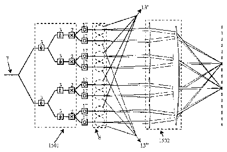
FIG. 15 illustrates another example of scanning system 116 that includes a
combined
multiplexing unit 1501 along with a first multiplexing unit 17 incorporated at
each output.
Similar to FIG. 12, a unique scan depth can be set for each output through the
use of
multiplexing units 17. In one example, combined multiplexing unit 1501
includes optical
switches 2 to select a subset (either 13' or 13") of active optical paths.
Also included are
optical modulators 3 for multiplexing the paths in the selected subset 13',
13" of active optical
paths, enabling simultaneous measurement of light contributions that have been
scattered by
the sample and collected by various output waveguides 8. First multiplexing
units 17 actuate
independently on each of the selected optical paths associated with each
output waveguide
8, allowing independent control of the scanning depth for each output.
In order to direct the beams associated with various subsets 13', 13", optical
focusing
elements 1502 are included downstream of the output waveguides 8. In an
embodiment,
optical focusing elements 1502 include a plurality of lenses as illustrated to
focus the beams
associated with a given subset onto the same region of the target sample. For
example,
optical focusing elements 1502 include a single large lens and a plurality of
smaller lenses,
with each smaller lens configured to collect beams of radiation from each
subset 13', 13".
Although only two subsets 13', 13" of optical paths are illustrated, it should
be understood
that any number of subsets may be generated via combined multiplexing unit
1501. In an
embodiment, the various beams in a given subset are considered to be directed
at the same
target region on the sample when the distance between the centers of each beam
in the
subset is lower than or equal to twice the diameter of each beam, when both
this distance
and this diameter are measured in the focal plane associated with optical
focusing elements
1502. The Full Width Half Maximum (FWHM) definition may be used, for example,
for
determining the diameter of the radiation beam. The illustrated embodiment
allows for
measurements of the sample with spatial diversity, e.g., measuring the same
region of the
sample from different directions. This reduces the noise in the image.
The embodiment in FIG. 15 permits the acquisition of information on the
angular
dependency of the sample scattering function, as it is possible to measure the
light that is
scattered by a sample region in different directions relative to the direction
of the incident
light. For example, when one of the beams produced from an output waveguide 8
reaches
the sample, part of the light will be scattered in different directions. The
light that is scattered
backwards relative to the incident light is redirected by optical focusing
elements 1502 back
CA 02836609 2013-11-19
WO 2012/160005
PCT/EP2012/059308
- 15 -
to the original output waveguide 8. However, according to an embodiment,
optical focusing
elements 1502 are configured to direct the beams from any given subset 13',
13" towards the
same sample region. Therefore, light scattered in directions other than
directly backwards
(relative to the incident light) may be directed by optical focusing elements
1502 to one of the
other output waveguides 8 belonging to the subset 13', 13". The total path
length traveled by
the light from the point where it exits the device through an output waveguide
8 until it is
collected by a different output waveguide 8, belonging to the same subset 13',
13", is
different for each output waveguide 8 belonging to the subset 13', 13". In an
embodiment,
this path length difference is accounted for via the adjustable scan depth
range on each
optical path using first multiplexing unit 17. As such, this embodiment allows
for the
simultaneous measurement of light scattered in different directions for the
same sample
region in a single interferometer, and the angular dependency of the
scattering function of
the sample can be obtained.
Figure 16 illustrates an example technique for scanning a sample both axially
and
laterally, according to an embodiment. The beams are represented in
geometrical optic
approximation by two lines corresponding to the lateral extension of the
optical energy. The
lines intersect with each other at a first approximation at a focal plane
1601. The axial scan is
performed using the OCT interferometric system described herein with the basic
scanning
range multiplication in multiplexed bands (for example, by using frequency
division
multiplexing). The diagonal lines that intersect pairwise represent light
beams corresponding
to each output waveguide 8, after focusing on the sample. The intersection
points define
focal plane 1601 associated with the lens system used. Laterally, time
division, frequency
division, or any other type of multiplexing is performed between the optical
paths, as
explained in previous embodiments. Axially, frequency division multiplexing
may be chosen
for selecting the scan depth in order to multiply the effect of the reference
arm of an
interferometric system. Thus, in embodiments, a scan is performed only within
a specified
section for a given frequency range (e.g., f, 2f, 3f, etc., as illustrated in
FIG. 16).
Another embodiment of scanning system 116 is illustrated in FIG. 17. In an
embodiment, a gradient index (GRIN) lens 1701 is included to focus the light
from output
waveguides 8 onto a sample. GRIN lens 1701 may be mounted contiguously to the
same
substrate associated with optical waveguides 8, or in a cavity etched into the
substrate,
where the various integrated waveguides are produced due to its compact size
and
substantially cylindrical shape. In another example, GRIN lens 1701 is
monolithically
integrated in the same substrate as output waveguides 8. The more compact
assembly
allows for the scanning system to be encapsulated with biocompatible and
sterilization-ready
materials to produce a medical sampling element, according to an embodiment.
The medical
CA 02836609 2013-11-19
WO 2012/160005
PCT/EP2012/059308
- 16 -
sampling element may be inserted into a catheter, needle, or other device or
medical
instrument of small size, for the study of small tissues in areas that are
typically difficult to
access. As previously discussed with regards to other focusing elements, the
distance
between adjacent beams corresponding to different output waveguides 8 is
sufficiently small
compared to the diameter of the beams, such that the information gathered
along the
adjacent beams can be reorganized later as a two-dimensional or three-
dimensional
rendered image of the sample. In one example, the distance between adjacent
beam
centers is within 1-10 times the diameter of a single beam, when both this
distance and this
diameter are measured in the focal plane of GRIN lens 1701. The Full Width
Half Maximum
(FWHM) definition may be used, for example, for determining the diameter of
the radiation
beam.
FIGs. 18A-B illustrate a top and side view, respectively, of scanning system
116,
according to an embodiment. In this embodiment, scanning system 116 includes a
reflecting
element 5 positioned downstream of GRIN lens 1701. In one example, reflecting
element 5
is a right angle prism, as illustrated in FIG. 18B. In this example,
reflecting element 5 may
direct one or more incoming radiation beams in a direction perpendicular to
the initial beam
direction from output waveguides 8. In an embodiment, scanning system 116 as
embodied
in FIG. 18A may be mounted in a catheter, where small movements of the device
along a
guide wire can be used to provide a 3D rendering of a blood vessel wall under
study.
Reflecting element 5 may be a separate component from the rest of scanning
system 116.
Alternatively, reflecting element 5 may be integrated into the same substrate
as either output
waveguides 8 or GRIN lens 1701. In another example, all of the illustrated
elements may be
monolithically integrated in the same substrate.
FIGs. 19A-B illustrate a top and side view, respectively, of scanning system
116,
according to an embodiment. In this embodiment, scanning system 116 includes
an
adjustable reflecting element 6 positioned downstream of GRIN lens 1701. In
one example,
adjustable reflecting element 6 is a mechanically adjustable reflector. The
inclusion of
adjustable reflecting element 6 allows for the generation of 3D images with
only a single low-
speed scanning axis, instead of having two. Indeed, the need for providing a
high-speed
scan of the sample is removed in such an embodiment, only serving for the
orientation of the
group of beams to the area to scan, or for providing the slow direction in a
three-dimensional
scan. Thus, to generate 3D images, only a single low-speed scanning axis is
needed,
instead of two, according to an embodiment. Adjustable reflecting element 6
may adjust the
reflected angle of the incoming beams of radiation via any suitable means, as
would be
known to one having skill in the relevant art(s). For example, adjustable
reflecting element 6
CA 02836609 2013-11-19
WO 2012/160005
PCT/EP2012/059308
- 17 -
may use coupled piezoelectric actuators or electrostatic actuation, or
mechanical rotation to
adjust the orientation of adjustable reflecting element 6.
FIGs. 20A-B illustrate a top and side view, respectively, of scanning system
116,
according to an embodiment. In this embodiment, scanning system 116 includes
an
adjustable reflector array 2001. Adjustable reflector array 2001 may be used
to probe
multiple images from various target regions of a sample. In an embodiment,
each produced
beam of radiation is associated with one reflecting element in adjustable
reflector array 2001.
Each element can be individually moved to change the reflection angle of the
incoming
associated radiation beam. This allows for a situation where each beam of
radiation is
targeted towards a different region of a sample.
In an embodiment, adjustable reflector array 2001 includes MEMS devices such
as
adjustable micro-mirrors. The micro-mirrors may be fabricated using
conventional
microfabrication techniques and integrated in the same substrate as either
output
waveguides 8 or GRIN lens 4. In another embodiment, adjustable reflector array
2001 may
be fabricated on a separate substrate and flip-chip bonded to the substrate
that includes
output waveguides 8 and GRIN lens 4. If each of the reflecting elements in
adjustable
reflector array 2001 provides independent transversal scanning, then the
scanning system is
capable of, for example, obtaining a large number of images either
sequentially or
simultaneously.
It should be understood that for the embodiments described above, the use of
GRIN
lens 1701 may be replaced by other suitable optical focusing elements to
achieve the same
result. Furthermore, although second multiplexing unit 9 is illustrated in the
embodiments
shown in FIGs. 17-20 as using time division multiplexing, it should be
understood that any
multiplexing technique, or combination of techniques, as described previously
could also be
used.
Although the above embodiments have been described in the context of an OCT
system, any of the various embodiments described above can also be applied to
other
applications. For example, any of the various embodiments described above can
be applied
to the optical reading of data stored in multilayer optical systems, where the
selection
between the layers is performed by detection systems based on an optical
coherence gating.
One example advantage provided in this case is the increase in reading speed,
when the
reading is (quasi-) simultaneous on a large number of optical tracks. It is
also to be noted
that any of the embodiments described above are susceptible to modifications
of detail,
provided that they do not alter the fundamental principle and the essence of
the invention.
CA 02836609 2013-11-19
WO 2012/160005
PCT/EP2012/059308
- 18 -
FIG. 21 illustrates an example method 2100 for performing lateral scanning,
according to an embodiment. Method 2100 may be performed, for example, by any
of the
various embodiments described above for scanning system 116.
At step 2102, a beam of radiation is received at a first multiplexing unit.
The first
multiplexing unit may be, for example, any one of the multiplexing units
described in regards
to FIGs. 4-6.
At step 2104, a group delay is introduced to the beam of radiation received at
the first
multiplexing unit based on an optical path traversed by the beam of radiation
received at the
first multiplexing unit among a first plurality of optical waveguides in the
first multiplexing unit.
The group delay may be introduced in a variety of ways, such as by using
waveguide
segments of different lengths or waveguide segments allowing modification of
the refractive
index by effects such as thermo-optical, electro-optical, charge injection,
etc. In one
example, optical modulating elements and/or optical switches are used to
differentiate the
beam among a plurality of paths, with each path having a unique group delay
associated with
it.
At step 2106, a beam of radiation is received by a second multiplexing unit.
The
beam of radiation received by the second multiplexing unit may be the same
beam of
radiation received by the first multiplexing unit, such as when the first
multiplexing unit is
located in the sample arm. Alternatively, the beam of radiation received by
the second
multiplexing unit may be different from the beam of radiation received by the
first multiplexing
unit, such as when the first multiplexing unit is located in the reference
arm. The second
multiplexing unit may be, for example, any of the various multiplexing units
described in
regards to FIGs. 7-13 or FIG. 15.
At step 2108, the beam of radiation received by the second multiplexing unit
is
differentiated among a second plurality of optical waveguides to produce one
or more output
radiation beams. The beam of radiation received by the second multiplexing
unit may be
differentiated among a variety of optical paths using any one, or a
combination of, time
division multiplexing, frequency division multiplexing, coherence domain
multiplexing, etc.
At step 2110, the one or more output radiation beams are guided towards a
sample.
The guiding may include focusing and/or redirecting the light, as described in
the
embodiments illustrated in, for example, FIGs. 14-15 and FIGs. 17-20.
It is to be appreciated that the Detailed Description section, and not the
Summary and
Abstract sections, is intended to be used to interpret the claims. The Summary
and Abstract
sections may set forth one or more but not all exemplary embodiments of the
present
invention as contemplated by the inventor(s), and thus, are not intended to
limit the present
invention and the appended claims in any way.
CA 02836609 2013-11-19
WO 2012/160005
PCT/EP2012/059308
- 19 -
Embodiments of the present invention have been described above with the aid of
functional building blocks illustrating the implementation of specified
functions and
relationships thereof. The boundaries of these functional building blocks have
been
arbitrarily defined herein for the convenience of the description. Alternate
boundaries can be
defined so long as the specified functions and relationships thereof are
appropriately
performed.
The foregoing description of the specific embodiments will so fully reveal the
general
nature of the invention that others can, by applying knowledge within the
skill of the art,
readily modify and/or adapt for various applications such specific
embodiments, without
undue experimentation, without departing from the general concept of the
present invention.
Therefore, such adaptations and modifications are intended to be within the
meaning and
range of equivalents of the disclosed embodiments, based on the teaching and
guidance
presented herein. It is to be understood that the phraseology or terminology
herein is for the
purpose of description and not of limitation, such that the terminology or
phraseology of the
present specification is to be interpreted by the skilled artisan in light of
the teachings and
guidance.
The breadth and scope of the present invention should not be limited by any of
the
above-described exemplary embodiments, but should be defined only in
accordance with the
following claims and their equivalents.