Note: Descriptions are shown in the official language in which they were submitted.
CA 02837742 2013-11-28
WO 2012/170457
PCT/US2012/040981
1
DESCRIPTION
TRANSPARENT INFRARED-TO-VISIBLE UP-CONVERSION DEVICE
CROSS-REFERENCE TO RELATED APPLICATION
The present application claims the benefit of U.S. Provisional Application
Serial No.
61/493,696, filed June 6, 2011, which is hereby incorporated by reference
herein in its
entirety, including any figures, tables, or drawings.
BACKGROUND OF INVENTION
Recently, light up-conversion devices have attracted a great deal of research
interest
because of their potential applications in night vision, range finding, and
security, as well as
semiconductor wafer inspections. Early near infrared (NIR) up-conversion
devices were
mostly based on the heterojunction structure of inorganic semiconductors,
where a
photodetecting and a luminescent section are in series. Fabrication of
infrared IR-to-visible
up-conversion devices based on inorganic compound semiconductors is
challenging because
of the lattice mismatch between the two types of semiconductor materials used
for
photodetectors and light-emitting diodes LEDs. Because of the high cost of
epitaxial grown
inorganic devices, inorganic devices have been restricted to fabrication of
small area
applications.
Other up-conversion devices tend to display efficiencies that are typically
very low.
For example, a NIR-to-visible light up-conversion device that integrates a LED
with a
semiconductor based photodetector has exhibited a maximum external conversion
efficiency
of only 0.048 (4.8%) W/W. More recently, a hybrid organic/inorganic up-
conversion device,
where an InGaAs/InP photodetector is coupled to an organic light-emitting
diode (OLED),
has displayed an external conversion efficiency of 0.7% W/W. Currently
inorganic and
hybrid up-conversion devices are expensive to fabricate and the processes used
for
fabricating these devices are not compatible with large area applications.
Efforts are being
made to achieve low cost up-conversion devices with high conversion
efficiencies, high
sensitivity, high gain, and high image fidelity. Additionally, a device where
the IR irradiation
enters from a one face and light exclusively exits from a second face is
desirable for many
applications such as night vision applications.
CA 02837742 2013-11-28
WO 2012/170457
PCT/US2012/040981
2
BRIEF SUMMARY
Embodiments of the invention are directed to transparent up-conversion devices
that
have a stacked layer structure. The layer include a transparent anode, at
least one hole
blocking layer, an IR sensitizing layer, at least one hole transport layer, a
light emitting layer,
at least onc electron transport layer, and a transparent cathode, The stacked
layer structure
can be less than a micron in thickness. Anodes can be chosen from any
appropriate
conducting material including: indium tin oxide (ITO), indium zinc oxide
(IZO), aluminum
tin oxide (ATO), aluminum zinc oxide (AZO); carbon nanotubes; or silver
nanovvires. Hole
blocking layers can be chosen from any appropriate material including: Ti02;
Zn0; BCP;
Bphen; 3TPYMB; or UGH2. IR sensitizing layer can be any appropriate material
including:
PbSe QDs; PbS QDs; PbSe film; PbS film; InAs film; InGaAs film; Si film; Ge
film; GaAs
film; perylene-3,4,9,1 0-tetracarboxylic-3 ,4,9, 1 0- dianhydride
(PTCDA); tin (II)
phthalocyanine (SnPe); SnPc:C60; aluminum phthalocyanine chloride (AlNCI);
AlPcCl:C60;
titanyl phthalocyanine (Ti0Pc); or Ti0Pc:C60. The hole transport layer can be
any
appropriate material including: 1,1 -bis [(di-4-tolylamino)phenyl]cyclohexane
(TAPC); N,N'-
diphenyl-N,N'(2-naphthyl)-(1,1'-pheny1)-4,4'-diamine (NPB); and N,N'-diphenyl-
N,N'-
di(m-toly1) benzidine (TPD). The light emitting layer can be any appropriate
material
including: tris-(2-phenylpyidine) iridium; Ir(ppy)3; poly-12-methoxy-5-(2'-
ethyl-hexyloxy)
phenylene vinylene] (MEH-PPV); iris-(8-hydroxy quinoline) aluminum (Alq3); or
iridium
(111) bi,s4(4,6-di-fluoropheny1)-pyridinate-N,C2'lpicolinate (FIrpic). The
electron transport
layer can be any appropriate material including: tris [3 -(3 -pyridy1)-me
sityl] borane
(3TPYMB); 2,9-D imethy1-4,7 -diphenyl- 1 , 1 0-phenanthroline (BCP); 4,7-
diphenyl- 1 ,1 0-
phenanthroline (BPhen); and tris-(8-hydroxy quinoline) aluminum (A1q3). The
cathode can
be Indium Tin Oxide (ITO), Indium Zinc Oxide (IZO), Aluminum Tin Oxide (ATO),
Aluminum Zinc Oxide (AZO), carbon nanotube, silver nanowire, an Mg:Al layer,
or any
appropriate transparent conductor,
In an embodiment of the invention, the up-conversion device further comprises
an
antireflective layer. In one embodiment the antireflective layer can be an
A1q3 layer having a
thickness of less than 200 nm. In another embodiment of the invention, the up-
conversion
device further comprises an IR pass visible blocking layer. The IR pass
visible blocking
layer can comprise a plurality of alternating layers of materials having
different refractive
indexes, such as alternating layers of Ta205 and SiO2.
CA 02837742 2013-11-28
WO 2012/170457
PCT/US2012/040981
3
BRIEF DESCRIPTION OF DRAWINGS
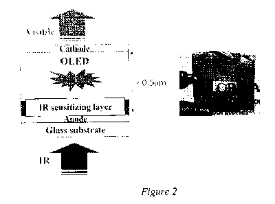
Figure 1 is a schematic diagram of a reflective infrared (IR) up-conversion
device.
Figure 2 is a schematic diagram of a transparent IR up-conversion device
having a
pair of transparent electrodes according to an embodiment of the invention.
Figure 3 is a schematic diagram of a transparent IR up-conversion device,
according
to an embodiment of the invention, where emitted visible light exits from two
surfaces of the
device.
Figure 4 is a schematic diagram of a transparent IR up-conversion device
including an
IR pass visible blocking layer to restrict emission of visible light to a
single exit face of the
stacked device according to an embodiment of the invention.
Figure 5 shows visible spectra of cathodes having 10:1 Mg:Ag with and without
antirefiective layers indicating the antirefiective layer for various
compositions.
Figure 6 is a schematic diagram of an exemplary transparent IR up-conversion
device
including an IR pass visible blocking layer, according to an embodiment of the
invention.
Figure 7 is a plot of luminescence for different applied voltages for the IR
up-
conversion device of Figure 6,
DETAILED DISCLOSURE
Embodiments of the invention are directed to transparent IR-to-Visible up-
conversion
devices having two electrodes that are transparent to visible light, also
indicated as visible or
light herein. In an embodiment of the invention, the output of the visible
light generated is
restricted from radiating out of the surface where the IR radiation, also
indicated as IR herein,
enters, even though visible light can enter from the surface, or face, where
the IR enters. A
typical reflective up-conversion device is shown in Figure I, where the source
IR enters and
the generated visible light exits the IR entry surface. A transparent up-
conversion device,
according to an embodiment of the invention, is shown in Figure 2, where an IR
sensitive
layer, situated on one side of an electrode, generates a charge carrier,
either an electron or a
hole, that under the bias of the device is directed to a light emitting layer
where the carrier
combines with its complementary charge carrier to generate visible light. As
shown in Figure
2, the up-conversion device is constructed with two transparent electrodes and
the visible
light, either that entering or that generated within the device, is
transmitted through the
opposite face of the IR entry surface of the device. However, as shown in
Figure 3, light
generated by the light emitting layer radiates in all directions from the
light emitting layer,
CA 02837742 2013-11-28
WO 2012/170457
PCT/US2012/040981
4
including the IR entry face of the device. To achieve high transparency the
entire up
conversion device is thin, comprising a series of layers, where the combined
layers, with the
exception of the substrate that supports the device and any IR pass visible
blocking layer, has
a thicknesses of less than about a micron, for example less than 0.5 microns
in thickness. The
supporting substrate can be, for example, a glass or a polymeric material that
is highly
transmissive of IR and visible light, and a second substrate can be used on
the face opposing
the first supporting substrate of the IR up-conversion device.
In embodiments of the invention, the IR sensitizing layer can be a broad
absorption IR
sensitizing layer comprising mixed PbSe QDs or mixed PbS QDs. In other
embodiments of
the invention, the IR sensitizing layer comprises a continuous thin film of:
PbSe, PbS, InAs,
InGaAs, Si, Ge, or GaAs. In other embodiments of the invention, the IR
sensitizing layer is
an organic or organometallic comprising material, such as, but not limited to:
perylene-
3,4,9,10-tetracarboxylie-3,4,9,10-dianhydride (PTCDA), tin (II) phthalocyanine
(SnPc),
SnPc:C60, aluminum phthalocyanine chloride (A1PcC1), A1PeCI:C60, titanyl
phthalocyanine
(Ti0Pc), and Ti0Pc:C60.
In an embodiment of the invention, the light emitting layer is an organic
light emitting
layer comprising fac-tris(2-phenylpyridine)iridium (Ir(ppy)3), which emits
green light at 515
nm. Other light emitting materials that can be employed in embodiments of the
invention
include, but are not limited to: poly-[2-methoxy, 5-(2'-ethyl-hexyloxy)
phenylene vinylene]
(MEH-PPV), tris-(8-hydroxy quinoline) aluminum (A1q3), and iridium (III) bis-
[(4,6-di-
fluoropheny1)-pyridinate-N,C2']picolinate (FIrpic).
In embodiments of the invention, an electron transport layer (ETL) is situated
between the light emitting layer and the cathode. The ETL comprises tris[3-(3-
pyridy1)-
mcsityl]borane (3TPYMB), 2,9-Dimethy1-4,7-dipheny1-1,10-phenanthroline (BCP),
4,7-
dipheny1-1,10-phenanthroline (BPhen), tris-(8-hydroxy quinoline) aluminum
(Alq3), or any
other appropriate material.
In embodiments of the invention, a hole transport layer (HTL), which is
situated
between the light emitting layer and IR sensitizing layer, comprises 1,1-
bisKdi-4-
tolylamino)phenylicyclohexane (TAPC), N,N'-diphenyl-N,N'(2-naphthyl)-(1,1'-
pheny1)-
4,4'-diamine (NPB), N,N'-diphenyl-N,N'-di(m-toly1) benzidine (TPD), or any
other
appropriate material.
In embodiments of the invention, a hole blocking layer (HBL) resides between
the
anode and the IR sensitizing layer. The HBL can be an inorganic HBL comprising
ZnO,
CA 02837742 2013-11-28
WO 2012/170457
PCT/US2012/040981
Ti02, or any other appropriate inorganic material. The HBL can be an organic
HBL
comprising, for example, 2,9-Dimethy1-4,7-dipheny1-1,10-phenanthroline (BCP) p-
bis(triphenylsilyl)benzene (UGH2), 4,7-dipheny1-1,10-phenanthroline (BPhen),
tris-(8-
hydroxy quinoline) aluminum (A1q3), 3,5'-N,N'-dicarbazole-benzene (mCP), C60,
or tris[3-
5 (3-pyridy1)-mesityl]borane (3TPYMB).
Transparent electrodes that can be employed at the IR entry surface, which is
shown
as the anode in Figure 3 or Figure 4, include, but are not limited to, indium
tin oxide (ITO),
indium zinc oxide (IZO), aluminum tin oxide (ATO), aluminum zinc oxide (AZO),
carbon
nanotube films, or silver nanowires. Transparent electrodes that can be
employed at the
visible exit surface, shown as the cathode in Figure 3 or Figure 4, include,
but are not limited
to, indium tin oxide (ITO), indium zinc oxide (IZO), aluminum tin oxide (ATO),
aluminum
zinc oxide (AZO), carbon nanotube, silver nanowire, or a Mg:Al layer. In one
embodiment
of the invention, a stacked 10:1 Mg:Ag layer with a thickness of less than
20nm is used as a
transparent electrode. In an embodiment of the invention, an anti-reflective
layer can be
situated on the exterior surface of the transparent electrode at the visible
exit surface. For
example, an Alq3 layer can be an anti-reflective layer that allows good
transparency when the
A1q3 layer is less than about 100 nm in thickness. Alternately, the
antireflective layer can be
a metal oxide, such as Mo03, of about 50 nm or less in thickness. In an
embodiment of the
invention, the electrode at the visible light exit surface comprises a 10:1
Mg:Al layer of about
nm and an Alq3 layer of 50 nm is situated upon the electrode. As shown in
Figure 5,
different cathodes having different thicknesses of 10:1 Mg:Ag layers, with
different thickness
of anti-reflective layers, illustrate the advantage of the antireflective
layer. As indicated in
Figure 5, the cathode can be thicker when the antireflective layer is present,
and excellent
transparency occurs for thin cathodes having antireflective layers up to about
50 nm in
thickness.
An up-conversion device according to an embodiment of the invention is shown
in
Figure 4, where, by including an IR pass visible blocking layer between the IR
entry face and
the LED layer, the device becomes visible light opaque at the IR entry face.
The IR pass
visible blocking layer absorbs and/or reflects visible light internally rather
than allowing
10 visible light loss through the IR entry face while permitting IR
radiation to pass through the
layer, as shown in Figure 4. The electrode closest to the IR entry face must
be IR transparent
to a high degree, with at least 50% transmittance, and the electrode closest
to the visible
detection face must be visible light transparent to a high degree, with at
least 50%
CA 02837742 2013-11-28
WO 2012/170457
PCT/US2012/040981
6
transmittance over the wavelength range that visible light is emitted from the
LED. In
embodiments of the invention having no IR pass visible blocking layer, the
device has at least
20% transmittance of light through the entire stack of layers. When the IR
pass visible
blocking layer has a reflective surface, an increase in the proportion of
visible light directed
to the light exiting face of the device is possible relative to a device
having no layer or a non-
reflective (light absorbing) IR pass visible blocking layer. The surfaces of
the up-conversion
device perpendicular to the stacked layers can be covered with an opaque
coating or
otherwise abutted to an opaque surface that is an absorbent and/or reflective
surface such that
visible light is not lost through the sides of the device. The position of the
IR pass visible
blocking layer, as shown in Figure 4, can be situated as a layer between the
substrate and
anode. The layer can also be situated on the surface of the substrate opposite
the anode, or,
when both layers have the appropriate electronic properties to act as an
interconnect layer or
as an active layer in the device, the IR pass visible blocking layer can be
situated between any
layers of the device on the IR entry side of the LED employed in the device.
The IR pass visible blocking layer used in the up-conversion device, according
to an
embodiment of the invention, can employ a multi dielectric stack layer. The IR
pass visible
blocking layer comprises a stack of dielectric films with alternating films
having different
refractive indices, one of high refractive index and the other of a
significantly lower
refractive index. An exemplary IR pass visible blocking layer is a composite
of 2 to 80
alternating layers of Ta205 (RI = 2.1) and Si02 (RI = 1.45) that are 10 to 100
nm in thickness.
METHODS AND MATERIALS
An exemplary up-conversion device according to an embodiment of the invention
is
shown in Figure 6. The device has a glass substrate upon which resides an IR
pass visible
mirror of 14 alternating layers of Ta205 and Sia) which are about 70 nm thick
on average
and a transparent ITO anode of about 100 nm in thickness. Upon the anode is
deposited a 30
nm film of ZnO as a HBL and a 100 nm thick layer of PBSe QDs as the IR
sensitizing layer.
The IR sensitizing layer is separated from a 30 nm thick 7% Irppy3 CBP light
emitting layer
by a HTL of 45 nm of TAPC. The light emitting layer is separated, by a
composite ETL of
20 nm of 3TPYMB and 25 nm of Bphen, from a 10 nm 10:1 Mg:Ag cathode, with a 50
nm
A1q3 anti-reflective layer on the opposite surface of the cathode. The up-
conversion device of
Figure 6 displays almost no luminescence in the dark, but from a threshold of
5 V to 15 V
undergoes about a 100 fold increase in luminescence, as shown in Figure 7.
CA 02837742 2013-11-28
WO 2012/170457
PCT/US2012/040981
7
All patents, patent applications, provisional applications, and publications
referred to
or cited herein are incorporated by reference in their entirety, including all
figures and tables,
to the extent they are not inconsistent with the explicit teachings of this
specification.
It should be understood that the examples and embodiments described herein are
for
illustrative purposes only and that various modifications or changes in light
thereof will be
suggested to persons skilled in the art and are to be included within the
spirit and purview of
this application.