Note: Descriptions are shown in the official language in which they were submitted.
CA 02838775 2013-12-09
W02012/167835 PCT/EP2011/059648
1
Method for energizing a chain-link converter, controller, computer
programs and computer program products
Field of the invention
The invention relates generally to the field of electric power
network devices, and in particular to static compensators based on
chain-link converters.
Background of the invention
STATCOM (Static Compensator) converters based on chain-link topology
are emerging technology nowadays. A three-phase chain-link
converter, being a voltage source converter (VSC) device, comprises
three phase legs, each phase leg comprising a number of series-
connected cell converters. Figure 1 illustrates such a three-phase
chain-link converter 1 comprising a voltage source converter 2. The
three phase legs are denoted L1, L2, L3 and are connected in a delta
arrangement, but are in other set-ups connected in a wye
arrangement. Each phase leg comprises a number of series-connected
converter cells, e.g. phase leg L1 comprises converter cells 10, 11,
12, ..., n. Each converter cell 10, 11, 12, ..., n, sometimes denoted
converter link, comprises four valves connected in a H-bridge
arrangement with a capacitor unit 13. Each valve comprises a
transistor switch 19, such as an insulated gate bipolar transistor
(IGBT) having a free-wheeling diode 20 (also denoted anti-parallel
diode) connected in parallel thereto.
The chain-link converter 1, and in particular each phase leg
thereof, is connected to an electrical power grid 14, in the
illustrated case a three-phase network, via a phase reactor 15.
Further, each phase leg is connected to the power grid 14 via a
starting resistor 17 connected in parallel with a switch 16 and via
an AC circuit breaker 18.
Generally, when the chain-link converter of this type is to be
energized and started, and using phase leg L1 as an example, the
circuit breaker 18 is switched so as to provide a current path from
the power grid 14, through the starting resistor 17, the phase
CA 02838775 2015-09-17
,
,
2
reactor 15 and through the diodes of the chain-link converter 1, thereby
charging the
capacitor 13. When the capacitor voltage has reached a predetermined level,
the
starting resistor 17 is short-circuited by closing the parallel connected
switch 16. The
capacitor voltage will then increase further and the switches become
controllable.
Start-up of such chain-link converters involves a number of considerations.
For
example, in WO 2010/051854 one aspect of start-up of converters is addressed.
In
this publication a method for starting a chain-link converter is disclosed,
wherein a
power source is connected to at least one converter cell of a phase leg,
thereby
improving the start-up e.g. by lessening the stress put on components such as
diodes.
In another aspect, during start-up of the chain-link converter, some of the
electronic
switches may be defective, they could for example being in open circuit or in
short-
circuit. If energizing the chain-link converter 1 by limiting in-rush currents
by means
of the phase reactor 15 only, failed electronic switches in open circuit may
be
exposed to a voltage level above their voltage withstand capability and thus
cause
other electronic switches to break down.
In view of the above, it would be desirable to provide start-up procedures of
chain-
link converters for avoiding cascading failure of other components.
Summary of the invention
An object of the invention is to provide a method for energizing a chain-link
converter addressing the above problem.
CA 02838775 2015-09-17
3
According to the present invention, there is provided a method for energizing
a
chain-link converter comprising one or more phase legs, each phase leg
comprising
a number of series-connected converter cells, each converter cell comprising
four
valves arranged in an H-bridge connection with a DC capacitor, and each valve
in
turn comprising a semiconductor switch in parallel with a diode, the method
comprising the following steps in listed order:
charging the DC capacitor of each converter cell to a voltage level below
their nominal voltage so that the semiconductor switches are controllable,
diagnosing the converter cells so as to detect failed components thereof,
discharging the DC capacitors of faulty cells,
bypassing faulty components in a controlled manner, and
charging the DC capacitors to their nominal voltage.
Preferably, the object is according to a first aspect of the invention
achieved by a
method in a controller for energizing a chain-link converter comprising one or
more
phase legs. Each phase leg comprises a number of series-connected converter
cells and each converter cell comprises four valves arranged in an H-bridge
connection with a DC capacitor. Each valve in turn comprises a semiconductor
switch in parallel with a diode. The method comprises the steps of: charging
the DC
capacitor of each converter cell to a voltage level at which the semiconductor
switches are controllable but below their nominal voltage; diagnosing the
converter
cells so as to detect failed components thereof; bypassing faulty components
in a
controlled manner; and charging the DC capacitors to their nominal voltage.
Preferably, in accordance with the invention, the current is limited by means
of a
starting resistor, and a monitoring of the chain-link converter cells is
performed at a
low voltage level in order to prevent damage to components thereof.
CA 02838775 2015-09-17
4
Preferably, in an embodiment, the step of charging comprises closing an AC
breaker arranged between a power network and the chain-link converter and
charging the DC capacitor through a starting resistor arranged between the AC
breaker and the chain-link converter.
Preferably, in an embodiment, the step of diagnosing comprises receiving, in
the
controller, data from converter cell control and protection units connected to
gate
units of the converter cells, and determining based on the data whether a
converter
cell comprises a faulty component.
In the above embodiment, faulty components may be identified by monitoring
voltage of healthy components.
Preferably, in an embodiment, the step of bypassing failed components
comprises
the sub-steps of: discharging the DC capacitors of converter cells diagnosed
to
comprise a faulty component; bypassing converter cells comprising faulty
component by providing an alternative current path through healthy components
thereof or by closing a switch arranged in parallel with the converter cell
comprising
the faulty component.
Preferably, in an embodiment, the method comprises the further step of closing
a
starting resistor switch arranged in parallel with a starting resistor, the
starting
resistor arranged between a power network and the chain-link converter,
whereby
the DC capacitors are charged to their nominal voltage.
Preferably, in an embodiment the voltage level at which the semiconductor
switches
are controllable comprises a voltage level at which they just become
controllable.
CA 02838775 2015-09-17
4a
Preferably, in different embodiments the phase legs are connected in a delta
configuration or in a wye configuration.
Preferably, in an embodiment, the method comprises the additional step of,
performed prior to the step of bypassing the faulty components, discharging
the DC
capacitors of faulty cells.
According to the present invention, there is also provided a controller for
energizing
a chain-link converter comprising one or more phase legs, each phase leg
comprising a number of series-connected converter cells, each converter cell
comprising four valves arranged in an H-bridge connection with a DC capacitor,
and
each valve in turn comprising a semiconductor switch in parallel with a diode,
the
controller arranged to enable the following steps in listed order:
enable the charging of the DC capacitor of each converter cell to a voltage
level at which the semiconductor switches are controllable but below their
nominal
voltage,
diagnose the converter cells so as to detect failed components thereof,
enable discharging of the DC capacitors of faulty cells,
enable bypassing of faulty components in a controlled manner, and
enable charging of the DC capacitors to their nominal voltage.
Preferably, the object is according to a second aspect of the invention
achieved by a
controller for energizing a chain-link converter comprising one or more phase
legs.
Each phase leg comprises a number of series-connected converter cells and each
converter cell comprises four valves arranged in an H-bridge connection with a
DC
capacitor. Each valve in turn comprises a semiconductor switch in parallel
with a
diode, the controller arranged to: enable the charging of the DC capacitor of
each
CA 02838775 2015-09-17
4b
converter cell to a voltage level at which the semiconductor switches are
controllable but below their nominal voltage; diagnose the converter cells so
as to
detect failed components thereof; enable bypassing of faulty components in a
controlled manner; enable charging the DC capacitors to their nominal voltage.
According to the present invention, there is also provided a non-transitory
computer
readable storage medium having recorded therein statements and instructions
for
execution by a controller for energizing a chain-link converter comprising one
or
more phase legs, each phase leg comprising a number of series-connected
1 0 converter cells, each converter cell comprising four valves arranged in
an H-bridge
connection with a DC capacitor, and each valve in turn comprising a
semiconductor
switch in parallel with a diode, the statements and instructions comprising
computer
program code, which, when run on said controller, causes the controller to
perform
the following steps in listed order:
enable the charging of the DC capacitor of each converter cell to a voltage
level at which the semiconductor switches are controllable but below their
nominal
voltage,
diagnose the converter cells so as to detect failed components thereof,
enable discharging of the DC capacitors of faulty cells;
20 enable bypassing of faulty components in a controlled manner, and
enable charging of the DC capacitors to their nominal voltage.
Preferably, the object is according to a third aspect of the invention
achieved by a
computer program for energizing such a chain-link converter. The computer
program comprises computer program code, which, when run on a controller,
causes the controller to perform the steps of: enable the charging of the DC
capacitor of each converter cell to a voltage level at which the semiconductor
CA 02838775 2015-09-17
4c
switches are controllable but below their nominal voltage; diagnose the
converter
cells so as to detect failed components thereof; enable discharging the DC
capacitor
of faulty cell; enable bypassing of faulty components in a controlled manner;
enable
charging the DC capacitors to their nominal voltage.
Preferably, the object is according to a fourth aspect of the invention
achieved by a
computer program product comprising a computer program as above and a
computer readable means on which the computer program is stored.
CA 02838775 2013-12-09
WO 2012/167835 PCT/EP2011/059648
Further features and advantages of the invention will become clear
upon reading the following description and the accompanying
drawings.
Brief description of the drawings
5 Figure 1 illustrates a prior art three-phase chain-link converter.
Figure 2 illustrates a delta-connected three-phase chain-link
converter, for which aspects of the invention may be implemented.
Figure 3 illustrates a flow chart over steps of a method in an
embodiment of the invention.
Figure 4 illustrates a wye-connected three-phase chain-link
converter, for which aspects of the invention may be implemented.
Figure 5 illustrates a controller for controlling a chain-link
converter.
Detailed description of embodiments
In the following description, for purposes of explanation and not
limitation, specific details are set forth such as particular
architectures, interfaces, techniques, etc. in order to provide a
thorough understanding of the invention. However, it will be
apparent to those skilled in the art that the invention may be
practiced in other embodiments that depart from these specific
details. In other instances, detailed descriptions of well-known
devices, circuits, and methods are omitted so as not to obscure the
description of the invention with unnecessary detail. Like reference
numerals refer to like elements throughout the description.
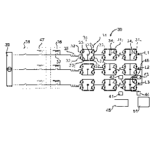
Figure 2 illustrates a delta-connected three-phase chain-link
converter, for which aspects of the invention may be implemented.
The three phase chain link converter 30 is of the type described
with reference to figure 1. In particular, the chain-link converter
comprises a voltage source converter having three phase legs L1,
30 L2, L3 connected in a delta arrangement. Each phase leg comprises a
number of series-connected converter cells. Taking phase leg L1 as
an example, it comprises converter cells 311, 312,¨, 31n, each
CA 02838775 2013-12-09
WO 2012/167835 PCT/EP2011/059648
6
converter cell comprising four valves connected in a H-bridge
arrangement with a capacitor unit 34. Each valve in turn comprises a
transistor switch 32, such as earlier mentioned IGBT, having a free-
wheeling diode 33 connected in parallel thereto. In the following
IGBT is used when describing aspects of the invention, but other
semiconductor devices could be used, e.g. gate turn-off thyristors
(GTO) or Integrated Gate-Commutated Thyristors (IGCT).
The phase leg L1 is connected to an electrical power grid 39, e.g. a
three-phase power grid, via a phase reactor 35. Further, the phase
leg L1 is connected to the power grid 39 via a starting resistor 36
connected in parallel with a starting resistor switch 37 and via an
AC circuit breaker 38. The other phase legs L2, L3 are arranged in a
corresponding manner.
A controller 50 is arranged to control the chain-link converter 1,
for example controlling the switching of the IGBTs of the converter
cells. Each IGBT of each converter cell is connected to a gate unit.
For example, the IGBTs of a converter cell 46 of phase leg L3 are
connected to a respective gate units 41, 42, 43, 44, which in turn
are connected to a converter cell control and protection unit 45.
The converter cell control and protection units (e.g. converter cell
control and protection unit 45 of phase leg L3) of a converter cell
are able to communicate with the controller 50, for example by being
connected to a communication bus (not illustrated).
In accordance with an aspect of the invention, a method is provided
enabling a safe start of the chain-link converter 30. Briefly,
faulty cells are detected and bypassed before the DC capacitors of
the chain-link converter are fully loaded. The chain-link converter
can then be operated with the faulty cells without risk of
subsequent failures of other components.
30 In accordance with an embodiment, the chain-link converter 30 is
energized in accordance with the following sequence, described for
the first phase leg L1 for rendering the description clear and
concise. The second and third phase legs L2, L3 of the chain-link
converter 30 are energized simultaneously in a corresponding manner.
CA 02838775 2013-12-09
WO 2012/167835 PCT/EP2011/059648
7
Upon energizing the chain-link converter 30, the main AC circuit
breaker 38 of phase leg L1 is closed, and the starting resistor
switch 37 connected in parallel with the starting resistor 36 is
open. Thereby the DC capacitors 341, 342,¨, 34n are charged at a low
voltage rate to a certain charging level. The charging level to
which the DC capacitors 341, 342,¨, 34. are charged is chosen so as
to just reach a voltage level at which the electronic switches (e.g.
IGBT 32) are controllable. As an example such voltage level could be
about 600 V for a component having a rated value of 2,4 kV. It is
realized that the voltage level depends on the rated value of the
component.
Failed converter cell components, e.g. electronic switches, are then
detected by means of the gate units 41, 42, 43, 44 and the converter
cell control and protection units and the controller 50. In
particular, the controller 50 receives data from the converter cell
control and protection unit 45, which in turn receives data from the
gate units 41, 42, 43, 44. The controller 50 is arranged to detect a
faulty component based on data, such as converter cell DC voltage or
converter cell AC current, or converter AC voltage received from
these units.
Upon detection of a fault, a zero output voltage mode is entered for
the converter cell having the faulty component. This is accomplished
by the controller 50 transmitting a control signal to this end. In
particular, the output voltage of the chain link converter 30 is
controlled by control signals that are applied to the converter
cells. The converter cells can be put in a zero voltage mode by the
controller 50 transmitting a control signal to this end, i.e.
transmitting a control signal so that a zero output voltage is
provided at the output voltage AC terminals of the converter cell.
The DC capacitors of the converter cells having faulty components,
if any, e.g. faulty electronic switches or gate units, are
discharged in a controlled manner. One way of discharging the DC
capacitor in a controlled manner is by initiating the zero voltage
mode of a healthy converter cell and by using a healthy component of
the faulty converter cell. The phase leg current is limited by means
of the charging resistor 36.
CA 02838775 2013-12-09
WO 2012/167835 PCT/EP2011/059648
8
The provision of a current path for the phase current in a failed
cell through a healthy IGBT in an opposite branch in parallel with
the failed IGBT (which is in short-circuit mode) is described in a
co-pending patent application entitled "Method in a voltage source
chain-link converter, computer programs and computer program
products" (PCT/EP2011/056153), and assigned to the same applicant as
the present application. In the same application, a way of
discharging the cell when the failed IGBT is in open-circuit mode is
described, wherein the DC capacitor of the cell is discharged by the
remaining three healthy IGBT if the failed IGBT is in open-circuit
mode.
Another way of discharging the DC capacitor of IGBT position having
faulty component is to provide an external power source for enabling
the discharging. In particular, the electronic circuitry controlling
the IGBT switches are powered from the voltage across the switches.
At low DC voltage, the electronic circuit will stop functioning and
external power is required to operate the switch at low voltage.
External power supply can be provided by a switch of a healthy
neighbor cell or through the fiber optic link connecting the
electronic board controlling the switch to the main control by means
of high energy laser light.
Once the voltage of the DC capacitors of the faulty converter cells
is zero, then a bypass mode is initiated for the faulty converter
cells, and the DC capacitor thereof is short-circuited by means of
the healthy electronic switches of the converter cell comprising the
faulty device.
The bypass of the faulty converter cells can be accomplished in
different ways.
The converter cells can alternatively be bypassed by a mechanical
bypass switch, which is closed when a faulty component of the
converter cell is detected, thus bypassing it. The control of such
mechanical switches can be accomplished by suitable software in the
controller 50. In particular, the controller 50 receives data from
the gate units 41, 42, 43, 44 and the converter cell control and
protection unit 45, as described earlier, and when detecting that a
CA 02838775 2013-12-09
WO 2012/167835 PCT/EP2011/059648
9
converter cell has a faulty component, a signal is sent to the
mechanical switch connected in parallel with this converter cell for
closing it, thereby bypassing the converter cell.
In the next step of the energizing sequence, the zero-voltage mode
of the healthy converter cells is disabled, and the DC capacitors of
these healthy converter cells are charged to their nominal voltage.
When the DC capacitors 341, 342,, 34n reach their nominal voltage,
the starting resistor switch 37 is closed thus short-circuiting the
starting resistor 36. The chain-link converter 30 is now ready to be
put into operation having all (if any) unhealthy converter cells
bypassed.
The above is summarized with reference to figure 3, illustrating a
flow chart over steps of a method in an embodiment of the invention.
The method 60 may be implemented in the controller 50 and be used
for energizing the chain-link converter 30 as described. The method
60 comprises the first step of charging 61 the DC capacitor 341,
342,", 34n of each converter cell 311, 312,", 31n to a voltage level
at which the semiconductor switches are controllable but which is
below their nominal voltage. This can be done by closing the AC
circuit breakers 38 at a low voltage rate and keeping the starting
resistor switches at open position. The starting resistors 36 limit
the current through the respective phase legs L1, L2, L3.
The method 60 comprises the second step of diagnosing 62 the
converter cells 311, 312,", 31n so as to detect faulty components
thereof. This is done as soon as the voltage level of the capacitors
is such that the semiconductor switches are controllable. The
converter cell earlier described control and protection units 45 and
the gate units 41, 42, 43, 44 of the converter cells 311, 312,", 31n
are used for this end. For example, the voltage of healthy
components can be monitored in order to identify faulty components.
For example, faulty IGBT may be detected by determining that there
is no communication between a main control and the IGBT control. A
faulty IGBT may be detected by voltage monitoring of healthy IGBT or
CA 02838775 2013-12-09
WO 2012/167835 PCT/EP2011/059648
by short-circuit detection of the healthy IGBT in the same leg
(short through detector).
The method 60 comprises the third step of bypassing 63 failed
components in a controlled manner. This can be done by firstly
5 discharging the DC capacitors 341, 342,-, 34n of converter cells
diagnosed to comprise a faulty component, and by then bypassing
converter cells 311, 312,_, 31n comprising faulty component by
providing an alternative current path through healthy components
thereof or by closing a switch arranged in parallel with the
10 converter cell 311, 312,_, 31n comprising the faulty component, as
described earlier.
The method 60 comprises the fourth step of charging 64 the DC
capacitors 341, 342,-, 34n to their nominal voltage. The starting
resistor switch 37 is closed, whereby the starting resistor 36 is
short-circuited and the DC capacitors 341, 342,-, 34n are charged to
their nominal voltage.
In an embodiment, the step of diagnosing 62 comprises:
- performing diagnostic of the control communication between the
main controller and each individual switch controls,
- initiating a zero-voltage output mode by turning on alternatively
one pair of switches connected to the same ac output terminal in
order to detect switches failing to turn on,
- initiating the zero-voltage mode by turning on alternatively the
other pair of switches connected to the same ac output terminal in
order to detect switches failing to turn on,
- if a failed switch is detected as open (not short-circuited) then
zero-voltage mode is completed by turning on the switch in the same
branch of the failed switch in order to discharge the dc capacitor.
- detection of a failed switch will immediately initiate zero-
voltage mode until the dc capacitor is fully discharged by
initiating zero-voltage mode using the pair of healthy switches
CA 02838775 2013-12-09
WO 2012/167835 PCT/EP2011/059648
11
- when the dc capacitor is zero (or close) then bypass mode is
initiated by turning on continuously the upper pair healthy switches
or lower pair healthy switches.
The method 60 may also comprise a step of discharging the DC
capacitors of faulty cells, which step would then preferably be
performed prior to the step of bypassing the faulty components.
It is noted that the pairs of starting resistor and switch (e.g.
starting resistor 36 and switch 37 of phase leg L1) can be arranged
in the delta side as illustrated in figure 2 or on the line side, as
illustrated by the box 47 drawn with dashed lines, comprising
starting resistor and switch pairs also drawn with dashed lines. If
the starting resistors and associated switches are connected in the
delta side (in series with the phase reactor), then the starting
resistor can be used for discharging the DC capacitors when the
chain-link converter is switched off.
Figure 4 illustrates a wye-connected three-phase chain-link
converter, for which aspects of the invention may be implemented. In
particular, figure 4 illustrates the three-phase chain-link
converter 30 connected in a wye arrangement and comprising a tuned
zero-sequence filter. The methods as described are also applicable
for such configuration.
Figure 5 illustrates means for implementing the methods as
described, and in particular the controller 50 for controlling a
chain-link converter as described. The controller 50 comprises a
processor 52, e.g. a central processing unit, microcontroller,
digital signal processor (DSP), etc., capable of executing
software instructions stored in a computer program product 54
e.g. in the form of a memory. The processor 52 is connected to
an input device 51, that receives inputs e.g. from the earlier
described converter cell control and protection units 45 connected
to gate units 41, 42, 43, 44 of the converter cells 311, 312,..., 31.
It is noted that although only one processor 52 is illustrated
in figure 5, the implementation may comprise distributed
hardware so that several CPUs are used rather than one when
CA 02838775 2013-12-09
WO 2012/167835 PCT/EP2011/059648
12
running the software. Likewise, although only one input device
51 is illustrated, there may be several input devices.
The described methods and algorithms or parts thereof for
energizing the chain-link converter 30 may be implemented e.g.
by software and/or application specific integrated circuits in
the processor 52. To this end, the controller 50 may further
comprise a computer program 53 stored on the computer program
product 54.
With reference still to figure 5, the invention also
encompasses such computer program 53 for handling energizing
of chain-link converters. The computer program 53 comprises
computer program code which when run on the controller 50, and
in particular the processor 52 thereof, causes the controller
50 to perform the methods as described.
A computer program product 54 is thus also provided comprising
the computer program 53 and computer readable means on which
the computer program 53 is stored. The computer program
product 54 can be any combination of read and write memory
(RAM) or read only memory (ROM). The computer program product
54 may also comprise persistent storage, which, for example
can be any single one or combination of magnetic memory,
optical memory, or solid state memory.