Note: Descriptions are shown in the official language in which they were submitted.
CA 02839475 2013-12-16
AUDIO SIGNAL TRANSFER DEVICE
FIELD
The present invention generally relates to an electronic technique field, and
more
particularly relates to an audio signal adapter device.
BACKGROUND
With the development of an audio signal coding/decoding technology, more and
more
electronic equipments transmitting data via an audio interface are produced.
For example, the
electronic equipment can be connected with a mobile communication device via a
low-resistance
voice coil type of loudspeaker interface (such as a headphone interface) of
the mobile
communication device (such as a mobile phone) for receiving an audio signal
output from the
mobile communication device.
As an output power of the low-resistance voice coil type of loudspeaker
interface is usually
very low, except the electronic equipment (such as a headphone) with low power
consumption,
the electronic equipment receiving the audio signal via the low-resistance
voice coil type of
loudspeaker interface generally needs to use an external power source or an
internal battery for
normal working, which increases a cost of the electronic equipment and
enlarges a volume of the
electronic equipment.
SUMMARY
The present disclosure provides an audio signal adapter device with a high
output power.
The present disclosure provides an audio signal adapter device, comprising: an
input port,
an output port, a boosting unit, a rectifying unit and a filtering unit,
wherein the input port
comprises a first audio signal input pin configured to receive an audio signal
sent by an audio
signal sending equipment and to output the audio signal to an input end of the
boosting unit; the
boosting unit is configured to boost the audio signal input from the input end
of the boosting unit,
and to output a boosted audio signal to an input end of the rectifying unit
via an output end of the
1
22483934.1
CA 02839475 2013-12-16
boosting unit: the rectifying unit is configured to rectify the boosted audio
signal input from the
input end of the rectifying unit to obtain a level, and to output the level to
an input end of the
filtering unit via an output end of the rectifying unit; and the filtering
unit is configured to filter
the level input from the input end of the filtering unit to obtain a direct
current level, and to
output the direct current level to a power supply output pin of the output
port via an output end
of the filtering unit.
Furthermore, the output port comprises an audio signal output pin connected
with the output
end of the boosting unit and configured to output the audio signal.
Furthermore, the output port comprises an audio signal output pin connected
with the first
audio signal input pin and configured to output the audio signal.
Furthermore, the input port further comprises a MIC pin configured to output a
signal to the
audio signal sending equipment connected with the MIC pin.
Furthermore, the boosting unit is a boosting transformer. comprising a primary
coil and a
secondary coil; one pin of the primary coil is used as the input end of the
boosting unit and
connected with the first audio signal input pin, and the other pin of the
primary coil is grounded;
and at least one output pin of the secondary coil is used as the output end of
the boosting unit and
connected with the input end of the rectifying unit, and a tap of the
secondary coil is grounded.
Furthermore, the rectifying unit comprises at least one diode, an anode of the
at least one
diode is connected with the input end of the rectifying unit, and a cathode of
the at least one
diode is connected with the output end of the rectifying unit.
Furthermore, the secondary coil of the boosting transformer comprises two
output pins; the
input end of the rectifying unit comprises two input pins; the two output pins
of the secondary
coil are connected with the two input pins of the rectifying unit
respectively; and the rectifying
unit comprises two diodes, and anodes of the two diodes are connected with the
two input pins of
the rectifying unit respectively.
Furthermore, the filtering unit comprises a capacitor; one end of the
capacitor is connected
with the input or output end of the filtering unit; and the input end of the
filtering unit is
connected with the output end of the filtering unit.
2
224839341
CA 02839475 2013-12-16
Furthermore, the audio signal adapter device further comprises a signal
amplifier, and the
audio signal output pin is connected with the output end of the boosting unit
via the signal
amplifier.
Furthermore, the audio signal adapter device further comprises a signal
amplifier, and the
audio signal output pin is connected with the first audio signal input pin via
the signal amplifier.
Furthermore, the first audio signal input pin comprises a left-channel pin and
a
right-channel pin.
Furthermore, the boosting unit is a boosting transformer, comprising a primary
coil and a
secondary coil; one pin of the primary coil is used as the input end of the
boosting unit and
connected with the first audio signal input pin, and the other pin of the
primary coil is grounded;
and one output pin of the secondary coil is used as the output end of the
boosting unit and
connected with the input end of the rectifying unit, and the other output pin
of the secondary coil
is grounded.
Furthermore, the rectifying unit comprises one diode, an anode of the diode is
connected
with the input end of the rectifying unit, and a cathode of the diode is
connected with the output
end of the rectifying unit.
Furthermore, the input port further comprises a second audio signal input pin;
the output
port comprises an audio signal output pin; and the audio signal output pin is
connected with the
second audio signal input pin and configured to output the audio signal.
Furthermore, the audio signal adapter device further comprises a signal
amplifier, and the
audio signal output pin is connected with the second audio signal input pin
via the signal
amplifier.
In conclusion, the embodiments of the present disclosure realize feeding
function via an
audio signal with a relatively low hardware cost. An electronic equipment (an
audio signal
receiving equipment), used in combination with the audio signal adapter device
(e.g., an audio
cable or an audio adapter) of the present disclosure, can obtain power while
receiving an audio
signal, which reduces a cost of the electronic equipment and decreases a
volume of the electronic
equipment.
3
22483934.1
CA 02839475 2013-12-16
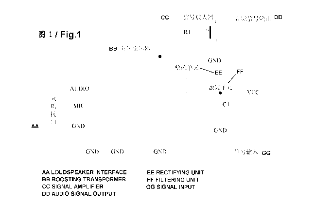
BRIEF DESCRIPTION OF THE DRAWINGS
Fig. 1 is a schematic diagram of an audio signal adapter device according to a
first
embodiment of the present disclosure;
Fig. 2 is a schematic diagram of an audio signal adapter device according to a
second
embodiment of the present disclosure;
Fig. 3 is a schematic diagram of an audio signal adapter device according to a
third
embodiment of the present disclosure;
Fig. 4 is a schematic diagram of an audio signal adapter device according to a
fourth
embodiment of the present disclosure; and
Fig. 5 is a schematic diagram of an audio signal adapter device according to a
fifth
embodiment of the present disclosure.
DETAILED DESCRIPTION
The present disclosure will be described below in detail with reference to
drawings and
embodiments.
The audio signal adapter device of the present disclosure may be an audio
cable, an audio
adapter cable, an audio adapter et.al.
FIRST EMBODIMENT
Fig. Ii is a schematic diagram of an audio signal adapter device according to
a first
embodiment of the present disclosure. As shown in Fig. 1, the audio signal
adapter device
comprises a loudspeaker interface, a boosting unit (such as a boosting
transformer shown in Fig.
1), a rectifying unit, a filtering unit, a power supply output pin (such as a
VCC pin shown in Fig.
1) and an audio signal output pin.
The loudspeaker interface connected with an audio signal sending equipment
(such as a
mobile phone) is configured to receive an audio signal output from the audio
signal sending
equipment.
4
22483934.1
CA 02839475 2013-12-16
The loudspeaker interface may be a low-resistance voice coil type of
loudspeaker interface
(such as a headphone interface), comprising: an audio signal input pin (such
as an AUDIO pin
shown in Fig. 1), and a ground pin (such as a GND pin shown in Fig. 1).
Furthermore, the loudspeaker interface may comprise a MIC pin configured to
output a
signal to the audio signal sending equipment connected with the MIC pin.
The audio signal input pin of the loudspeaker interface connected with one pin
of a primary
coil of the boosting transfaimer is configured to receive the audio signal
sent by the audio signal
sending equipment (such as the mobile phone) and to output the audio signal to
the one pin of the
primary coil. The ground pin of the loudspeaker interface is grounded.
Alternatively, in order to reduce a power consumption of the audio signal
sending
equipment., a resistor It2 (not shown in Fig. 1) may be connected in series
between the audio
signal input pin and the boosting transformer.
The boosting transformer comprises the primary coil and a secondary coil, and
is configured
to raise an input voltage (commonly about IV) at an input end (the primary
coil) to an output
voltage (for example, larger than or equal to 5V) at an output end (the
secondary coil).
The primary coil of the boosting transformer has two pins, one pin is
connected with the
audio signal input pin of the loudspeaker interface, and the other pin is
grounded. =
The output coil (i.e. the secondary coil) of the boosting transformer has two
output pins and
one tap, the two output pins are connected with two input pins of an input end
of the rectifying
unit respectively, and the tap is grounded.
The rectifying unit has the input end and an output end, and is configured to
rectify an
alternating current level input from the input end thereof, and to output the
rectified level via the
output end thereof
In this embodiment, the rectifying unit has two input pins of the input end,
and one output
pin of the output end. Accordingly, the rectifying unit comprises two diodes,
positive poles of the
two diodes are connected with the two input pins of the rectifying unit
respectively, and negative
poles of the two diodes are connected with the output pin of the rectifying
unit.
The filtering unit has an input end and an output end, and is configured to
convert the
5
22483934.1
CA 02839475 2013-12-16
rectified level input from the input end to a smooth direct current level, and
to output the smooth
direct current level via the output end.
In this embodiment, the input end of the filtering unit is connected with the
output end of
the rectifying unit, and the output end of the filtering unit is used as (or
connected with) the
power supply output pin to supply power to an electronic equipment connected
with the filtering
unit or a function module of the electronic equipment.
In this embodiment, the input end and the output end of the filtering unit are
connected, and
the filtering unit comprises a capacitor Cl. one end of which is connected
with the input/output
end of the filtering unit, and the other end of which is grounded.
Furthermore, in this embodiment, the audio signal output pin connected with
one output pin
of the output coil of the boosting transformer is configured to output the
audio signal.
Alternatively, a signal amplifier may be connected between the audio signal
output pin and
the output pin of the output coil of the boosting transformer, that is, an
input end of the signal
amplifier is connected with one output pin of the output coil of the boosting
transformer, and an
output end of the signal amplifier is used as (or connected with) the audio
signal output pin to
output an amplified audio signal.
As shown in Fig. 1, in this embodiment, the signal amplifier comprises a
resistor RI and an
NPN-type triode. One end of the resistor RI is connected with the input end of
the signal
amplifier, the other end of the resistor R1 is connected with a base (B) of
the NPN-type triode, a
collector (C) of the NPN-type triode is connected with the output end of the
signal amplifier, and
an emitter (E) of the NPN-type triode is grounded.
Alternatively, the signal amplifier comprises a resistor R1 and a PNP-type
triode. One end
of the resistor R1 is connected with the input end of the signal amplifier,
the other end of the
resistor RI is connected with a collector (C) of the PNP-type triode, a base
(B) of the PNP-type
triode is connected with the output end of the signal amplifier, and an
emitter (E) of the
PNP-type triode is grounded.
SECOND EMBODIMENT
6
22483934.1
CA 02839475 2013-12-16
Fig. 2 is a schematic diagram of an audio signal adapter device according to a
second
embodiment of the present disclosure. As shown in Fig. 2, the differences
between the second
embodiment and the first embodiment are as follows.
The audio signal output pin is connected with the audio signal input pin of
the loudspeaker
interface.
Alternatively, a signal amplifier may be connected between the audio signal
output pin and
the audio signal input pin of the loudspeaker interface, that is, an input end
of the signal
amplifier is connected with the audio signal input pin, and an output end of
the signal amplifier is
used as (or connected with) the audio signal output pin to output an amplified
audio signal.
THIRD EMBODIMENT
Fig. 3 is a schematic diagram of an audio signal adapter device according to a
third
embodiment of the present disclosure. As shown in Fig. 3, the differences
between the third
embodiment and the first embodiment are as follows.
In the third embodiment of the present disclosure, only one output pin of the
secondary coil
of the boosting transformer is connected with the input pin of the rectifying
unit. Thus, the
rectifying unit has only one input pin and comprises only one diode.
Apparently, compared with the first embodiment, by using this embodiment,
although a half
power of the secondary coil of the boosting transformer will be lost, a
circuit structure may be
simplified and a hardware cost may be reduced.
In this embodiment, the other output pin of the secondary coil of the boosting
transformer is
grounded, and a tap is not included in the boosting transformer.
FOURTH EMBODIMENT
Fig. 4 is a schematic diagram of an audio signal adapter device according to a
fourth
embodiment of the present disclosure. As shown in Fig. 4, the differences
between the fourth
embodiment and the first embodiment are as follows.
In the fourth embodiment, the audio signal input pin of the loudspeaker
interface comprises
7
22483934.1
CA 02839475 2013-12-16
a left-channel pin and a right-channel pin, which are connected with the same
pin of the primary
coil of the boosting transformer.
FIFTH EMBODIMENT
Fig. 5 is a schematic diagram of an audio signal adapter device according to a
fifth
embodiment of the present disclosure. As shown in Fig. 5, the differences
between the fifth
embodiment and the fourth embodiment are as follows.
In the fifth embodiment, the audio signal input pin of the loudspeaker
interface comprises a
left-channel pin and a right-channel pin. The left-channel pin connected with
the input end of the
signal amplifier is configured to output an audio signal, and the right-
channel pin connected with
one pin of the primary coil of the boosting transformer is configured to
output power.
Certainly, alternatively, the right-channel pin connected with the input end
of the signal
amplifier is configured to output an audio signal, and the left-channel pin
connected with one pin
of the primary coil of the boosting transformer is configured to output power.
The embodiments of the present disclosure realize feeding function via an
audio signal with
a relatively low hardware cost. An electronic equipment, used in combination
with the audio
signal adapter device of the present disclosure, can obtain power while
receiving an audio signal,
which reduces a cost of the electronic equipment and decreases a volume of the
electronic
equipment.
Certainly, according to a basic principle of the present disclosure, the
loudspeaker interface
in above embodiments may be replaced by other types of input ports having an
audio signal input
pin, a MIC pin and a ground pin.
Furthermore, the above input port may be fixedly connected with the audio
signal sending
equipment.
Furthermore, the above output port may be fixedly connected with the
electronic equipment
(the audio signal receiving equipment).
The above input port may comprise a plurality of plugs, such as an audio
signal plug
comprising the audio signal input pin and a MIC plug comprising the MIC
22483934.1