Note: Descriptions are shown in the official language in which they were submitted.
CA 02840012 2013-12-19
WO 2013/007984 PCT/GB2012/051563
1
Transformer for an inverter system
and an inverter system comprising the transformer
[0001] This invention relates to a transformer for an inverter system
and an inverter system comprising the transformer.
BACKGROUND
[0002] Modern power electronics systems, that require conversion of AC power
from an
electricity utility company AC supply to DC power for use by a process,
frequently use a
Switched Mode Power Supply (SMPS) for the required inversion.
[0003] A typical known SMPS 10 as illustrated in Figure 1 comprises an
inverter 11 which has
input ports electrically connected by first leads 120 to an AC energy source
12 to generate a
higher frequency AC inverter drive waveform 112, shown in a first inset 111 of
Figure 1, which
is fed from an output of the inverter 11 via second leads 110 towards a 1:N
XFMR transformer
rectifier unit 13. A secondary winding 133 of the transformer is connected by
leads 130 to Dn
diodes 14 to provide a desired DC voltage trace 162, shown in a second inset
161 of Figure 1,
across a load 16. For reasons explained below, an Ll common mode inductor 18
is connected
in series between the inverter 11 and the transformer rectifier unit 13, so
that the output leads
110 from the inverter are connected to an input of the L1 common mode inductor
18 and output
leads 150 from the inductor 18 electrically connect the inductor 18 to a
primary winding 131 of
the transformer 13.
[0004] As shown in Figure 1, a first stray capacitance Cs1 exists between
earth and the first
leads 120 connecting the energy source 12 to the inverter 11. A second stray
capacitance Cs2a
exists between the primary winding 131 and a core or former 132 of the
transformer rectifier
unit 13. A third stray capacitance Cs3a exists between the primary winding 131
and the
secondary winding 133 of the transformer rectifier unit 13 and a fourth stray
capacitance Cs4a
exists between the core or former 132 and the secondary winding 133 of the
transformer
rectifier unit 13.
[0005] The Dn diodes 14 are connected across the output terminals of the
secondary winding,
typically, but not restricted to, a bridge rectifier arrangement, 133 and an
Rmon monitor
resistance 15 is connected in series between earth and a first terminal of the
Dn diodes 14
connected to a first output terminal of the secondary winding 133, to monitor
load current
pulses, a corresponding voltage trace 152 across the monitor resistance 15
being illustrated in
a third inset 151 of Figure 1. The load 16 is connectable between the second
output terminal of
the Dn diodes 14 and earth.
CA 02840012 2013-12-19
WO 2013/007984 PCT/GB2012/051563
2
[0006] With high power systems, for example with a DC output power above 30kW,
the
SMPS 10 and the XFMR transformer rectifier unit 13 with diodes 14 can be
physically large, for
example greater than 250 litres, so that stray capacitances Cs1 and Cs2a to
Cs4a of the
various component parts are significant, for example greater than 10nF.
[0007] Separation between such large volume items is also typically large, for
example
3 metres or more, and with this length of electrical connectors 110, 120, 130,
150
therebetween, stray inductance of, for example, 2 or 3 pH is introduced.
[0008] The inverter drive waveforms 112 are pulsed and their rise and fall
times Tr and Tf,
can be relatively rapid, for example of the order of 1ps or less. The inverter
output peak
voltages Epk, shown in the first inset 111, typically have values up to lkV.
[0009] Stray currents I are related to the stray capacitance C and rise and
fall rates dV/dt by
the formula:
I = C * dV/dt,
so for lOnF stray capacitance and a 1ps rise time from zero to lkV, the peak
resultant stray
.. current is of the order of 10A.
[0010] These stray currents flow through the connector leads 110, 120, 130,
150 which, as
indicated above, are typically several metres long, presenting a very high
risk of EMC problems,
both internal to subsystems of the inverter and externally to co-located or
adjacent equipment.
[0011] As shown in Figure 1, in an attempt to reduce the impact of this stray
current, an L1
common mode choke 18 is often used between the inverter 11 and the transformer
rectifier unit
13 to reduce an amplitude of first stray current pulses, Isla, that flow in a
loop from earth
through the first stray capacitance Csl, the inverter 11 and via the second
and third stray
capacitances Cs2a, Cs3a, the XFMR windings 132, 133 and the Rmon monitor
resistor 15 back
to earth.
[0012] In applications where inverters are used to drive electric motors,
these currents flowing
in stray capacitances have been known to be sufficient to damage insulation
and bearings of
the motor. Moreover, unlike a motor, the diodes Dn of an XFMR provide a
potential source of a
second stray current Is2a.
[0013] There are many well-known arrangements of rectifiers for converting AC
signals to DC
signals or uni-directional pulses. In all cases, as the current in the Dn
rectifier diodes 14 falls to
zero and the voltage across them reverses, a "recovery current", as the diode
re-establishes
reverse voltage blocking, can produce very rapid transients. These reverse
currents form a
second stray current Is2a that flows through the fourth stray capacitance Cs4,
the secondary
CA 02840012 2013-12-19
WO 2013/007984 PCT/GB2012/051563
3
winding 133 of XFMR transformer 13 and the Rmon monitor resistance 15 to add
to the
problem of undesirable noise voltages.
[0014] The net result, at the very least, is that the voltage across Rmon
monitor resistance 15
is distorted with significant transient voltages Vb and -Vc on the leading and
trailing edges of
the pulses as shown in the third inset 151 of Figure 1. This can disturb
current monitoring
signals that may be required to be monitored precisely for process control,
and, in addition, the
voltages developed across the stray capacitances Cs1 and Cs2a to Cs4a of
residual elements
may put excessive stress on dielectric materials used in the construction of
XFMR transformer
13.
[0015] Furthermore, the stray capacitances Cs2a to Cs4a are not simple
capacitances in that
they represent the capacitance of transformer windings to surrounding
structures and as such
will have significant inductance in series with the capacitance. This further
complicates the
situation and it is frequently found that transient voltages Vb and Vc in the
Rmon monitoring
resistance 15 manifest themselves as large amplitude, high frequency,
typically 0.2 to 5 MHz,
damped oscillations that can persist for a large portion of a pulse duration.
[0016] The use of an electrostatic screen in a transformer is known: for
example, in a
transformer described in the Applicant's international patent application WO
2010/013049, such
an electrostatic screen is used. However, this is not completely effective in
the present
application because there are two predominant paths as described above in
which the currents
Isla and Is2a in stray capacitances Cs1 and Cs2a to Cs4a can flow.
[0017] It is desirable to reduce effects of these stray currents.
BRIEF SUMMARY OF THE DISCLOSURE
[0018] In accordance with a first aspect of the present invention there is
provided a
transformer comprising: primary winding means; secondary winding means; first
electrostatic
screen means located between the primary winding means and the secondary
winding means
and most proximate to the primary winding means; and second electrostatic
screen means
located between the primary winding means and the secondary winding means and
most
proximate to the secondary winding means, wherein the first electrostatic
screen means is
electrically connectable directly by a first lossy impedance to a power supply
electrically
connectable to the primary winding means and the second electrostatic screen
means is
electrically connectable directly by a second lossy impedance to a load
electrically connectable
to the secondary winding means.
CA 02840012 2013-12-19
WO 2013/007984 PCT/GB2012/051563
4
[0019] Conveniently, the transformer further comprises at least one rectifying
means
connected across the secondary winding means wherein the second electrostatic
screen
means is electrically connectable to the at least one rectifying means .
[0020] Advantageously, the first electrostatic screen means is connectable to
the power
supply via a first lossy impedance and the second electrostatic screen means
is connectable to
the load or the at least one rectifying means, respectively, via a second
lossy impedance.
[0021] Conveniently the secondary winding means comprises a plurality of
coaxially arranged
toroidal closed magnetic circuit means connected in series on a common axis
within an
enclosure means; the primary winding means comprises a plurality of turns
including electrically
conducting members passing axially through the toroidal closed magnetic
circuit means
electrically connected respectively to electrically conducting strip line
means located on outer
faces of walls of the enclosure means to form a continuous electrical
conductor, and the first
and second electrostatic screen means, located between the primary winding
means and the
secondary winding means, are provided by layered members comprising an
insulating support
layer sandwiched between first and second electrically conducting layers.
[0022] Conveniently, the first electrostatic screen means comprises an inner
electrically
conducting layer of a tubular first layered member located between the
electrically conducting
members forming a portion of the primary winding means passing axially through
the toroidal
closed magnetic circuit means and the toroidal closed magnetic circuit means
forming the
secondary winding means and outer electrically conducting layers of respective
planar layered
members located on inner faces of the enclosure means opposed to the outer
faces along
which the electrically conducting strip line means forming a further portion
of the primary
winding means are located.
[0023] Conveniently, the second electrostatic screen means comprises an outer
electrically
conducting layer of the tubular first layered member and inner electrically
conducting layers of
the respective planar layered members.
[0024] Conveniently, the tubular layered member comprises a first longitudinal
slit in the first
electrically conducting layer and a second longitudinal slit in the second
electrically conducting
layer to minimise eddy currents in the tubular layered member.
[0025] Advantageously, the first longitudinal slit is circumferentially offset
from the second
longitudinal slit.
[0026] Conveniently, the electrically conducting members forming a first
portion of the primary
winding are mutually spaced apart such that cross-sections of the electrically
conducting
members lie substantially on a circumference of a circle on a transverse cross-
section of the
enclosure means.
CA 02840012 2013-12-19
WO 2013/007984 PCT/GB2012/051563
[0027] Conveniently, the electrically conducting members forming the first
portion of the
primary winding are at least one of tubes, rods and strip conductors.
[0028] Advantageously, the electrically conducting members forming the first
portion of the
primary winding are tubes with a wall thickness comparable to a skin depth of
the electric
5 current carried thereby at an operating frequency of the transformer.
[0029] Alternatively, the electrically conducting members forming the first
portion of the
primary winding are flat strip conductors that have a thickness comparable to
a skin depth of
the electric current carried thereby at an operating frequency of the
transformer.
[0030] Advantageously, the electrically conducting members forming the first
portion of the
.. primary winding comprise a combination of electrically conducting members
connected in
parallel, each conducting member with a wall thickness comparable to a skin
depth of the
electric current carried thereby at an operating frequency of the transformer.
[0031] Conveniently, the electrically conducting strip line means forming a
second portion of
the primary winding are formed in printed circuit boards located on outer
faces of walls of the
enclosure means.
[0032] Conveniently, the enclosure means has a substantially rectilinear
transverse cross-
section and the walls of the enclosure means parallel to a longitudinal axis
of the enclosure
means are substantially planar.
[0033] Conveniently, the electrically conducting strip line means forming the
second portion of
the primary winding are located on first, second and third walls of the
substantially planar walls
of the enclosure means and have a thickness greater than a skin depth at an
operating
frequency of the transformer.
[0034] Conveniently, a fourth substantially planar wall of the enclosure means
comprises a
printed circuit board for rectifying means.
[0035] Advantageously, the transformer further comprises insulating tube means
on which the
secondary toroidal closed magnetic circuit means are located arranged to
provide voltage hold
off for the electrically conducting members forming the first portion of the
primary winding
passing axially through the toroidal closed magnetic circuit means.
[0036] Advantageously, the transformer further comprises coolant distribution
means.
[0037] Conveniently, the coolant distribution means comprises tube means,
coaxial with, and
of smaller diameter than, core apertures of the toroidal closed magnetic
circuit means, the tube
means being supplied with bleed hole apertures to direct the coolant towards
respective
secondary toroids.
CA 02840012 2013-12-19
WO 2013/007984 PCT/GB2012/051563
6
[0038] Advantageously, the transformer further comprises electrically
insulating sheet means
located between the toroidal closed magnetic circuit means and the planer twin-
thin walled
members to provide high voltage insulation and minimise a risk of high voltage
tracking across
a surface of the insulator.
-- [0039] Conveniently, the individual secondary toroidal closed magnetic
circuit means are
interconnected such that each secondary toroidal closed magnetic circuit means
of the
transformer is star connected and provides an input to a two pulse rectifier.
[0040] Conveniently the transformer is arranged for three-phase current and
comprises a first,
a second and a third primary winding means and a corresponding first, second
and third
secondary winding means arranged for the three phases respectively, and a
first and second
electrostatic screen means between the first primary and secondary winding
means, a third
and fourth electrostatic screen means between the second primary and secondary
winding
means and a fifth and sixth electrostatic screen means between the third
primary and
secondary winding means wherein the first, third and fifth electrostatic
screen means are
electrically interconnected and the second, fourth and sixth electrostatic
screen means are
electrically interconnected.
[0041] According to a second aspect of the invention there is provided an
inverter system
comprising a transformer as described above.
[0042] Conveniently, in the inverter system output ports of an inverter are
electrically
connected to the primary winding means of the transformer and the first
electrostatic screen
means is electrically connected to an input port of the inverter via a first
impedance such that a
first stray current flowing through a first stray capacitance between the
primary winding means
and the first electrostatic screen means flows through the first impedance to
the inverter.
[0043] Advantageously, the first impedance is sufficiently lossy that
substantially all of the
energy associated with the first stray current is dissipated in the first
impedance.
[0044] Conveniently, output ports of the inverter are electrically connected
to the primary
winding means via an inductance forming a common mode choke between the
inverter and
primary winding means.
[0045] Conveniently, at least one rectifying means is electrically connected
across the
secondary winding means of the transformer and the second electrostatic screen
means is
electrically connected to the at least one rectifying means via a second
impedance such that a
second stray current flowing through a second stray capacitance between the
secondary
winding means and the second electrostatic screen means flows through the
second
impedance and the at least one rectifying means
CA 02840012 2013-12-19
WO 2013/007984 PCT/GB2012/051563
7
[0046] Advantageously, the second impedance is sufficiently lossy that
substantially all of the
energy associated with the second stray current is dissipated in the second
impedance.
[0047] Conveniently, a monitor resistance is connected in series with a load
electrically
connectable to the secondary winding of the transformer to monitor a current
passing through
the load, and at least one of the first and second electrostatic screen means
substantially
prevents a first stray current which passes thorough a first stray capacitance
between the
primary winding means and the first electrostatic screen means and a second
stray current
which passes thorough a second stray capacitance between the secondary winding
means and
the second electrostatic screen means respectively from also passing through
the monitor
resistance.
[0048] According to a third aspect of the invention, there is provided a three-
phase inverter
system, comprising three individual and isolated transformers as described
above, wherein the
primary winding means of the transformers are delta connected and arranged to
be fed from a
three-phase inverter.
[0049] Conveniently, the secondary toroidal closed magnetic circuit means of
the three
individual and isolated transformers are interconnected such that each
secondary toroidal
closed magnetic circuit means of a transformer is star connected and provides
an input to a six
pulse rectifier.
BRIEF DESCRIPTION OF THE DRAWINGS
[0050] Embodiments of the invention are further described hereinafter with
reference to the
accompanying drawings, in which:
Figure 1 is a schematic diagram of a known Switched Mode Power Supply;
Figure 2 is a schematic diagram of a Switched Mode Power Supply according to a
first
embodiment of the invention;
Figure 3 is a schematic diagram of a three-phase Switched Mode Power Supply
according to a second embodiment of the invention; and
Figure 4 is a schematic cross-section of a transformer suitable for use in the
three-
phase Switched Mode Power Supply of Figures 2 or 3.
DETAILED DESCRIPTION
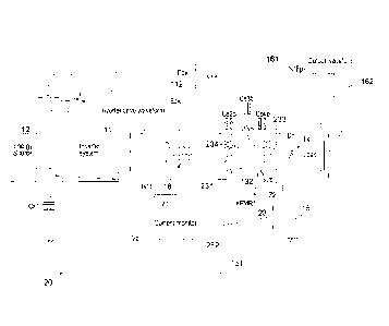
[0051] In a Switched Mode Power Supply (SMPS) 20 according to the invention,
illustrated in
a simplified form in Figure 2, the arrangement is basically the same as in
Figure 1, and the
same or corresponding reference signs are used for the same or corresponding
components
respectively where appropriate. However, in addition, the transformer
rectifier unit 23 of SMPS
CA 02840012 2013-12-19
WO 2013/007984 PCT/GB2012/051563
8
20 differs from the known transformer rectifier unit of SMPS 10 of Figure 1 by
being provided
with first and second electrostatic screens 234, 235. The first electrostatic
screen 234 is within
the core 132 located between the primary winding 231 and the secondary winding
233, but
proximate the primary winding 231 and the second electrostatic screen 235 is
located within the
core 132 between the primary winding and the secondary winding, but proximate
the secondary
winding of the transformer 23. Moreover, a first impedance Z1 is electrically
connected between
the first electrostatic screen 234 and an input of the inverter 11. A second
impedance Z2 is
electrically connected between the second electrostatic screen 235 and a node
between the
rectifier diodes 14 and the current monitor resistor 15. The first and second
electrostatic
screens 234, 235 allow separate return paths in which stray currents may flow.
The first stray
current !sib can now be made to flow back to its primary source, the inverter
11, via the first
impedance Z1 and the inductance L1 as a common mode choke 18, instead of
through the
secondary winding and monitor resistance 15 to earth, as in the prior art of
Figure 1. Similarly
the rectifier commutation current spikes Is2b can be made to flow around the
secondary
winding circuit 233 via the second Impedance Z2, instead of flowing through
the monitor
resistance 15 as in Figure 1. Thus the effect of the stray currents on the
current monitor
resistance 15 are avoided, or at least significantly reduced, as shown in the
voltage trace 252 of
the third inset 251 of Figure 2.
[0052] As described above in reference to Figure 1, the capacitance paths,
though now
controlled by the electrostatic screens 234, 235 do have series inductance due
to the
distributed nature of the windings 231, 233.
[0053] To provide adequate damping, the impedances L1, Z1, and Z2 should be
made lossy,
so that the energy associated with the stray currents is dissipated as heat in
these components.
[0054] High power systems typically use multiphase, often 3-phase, inverter
systems. Figure
3 shows an embodiment of an inverter system according to the invention for a 3-
phase system
such as described in international patent application WO 2008/149133. In this
arrangement
each transformer limb Tlp:T1s, T2p:T2s and T3p:T3s has a first electrostatic
screen 2341,
2342, 2343 proximate each of the primary windings Tip, T2p and T3p
respectively and a
second electrostatic screen 2351, 2352, 2353 proximate each of the secondary
windings T1s,
T2s and T3s respectively. The first electrostatic screens for the primary
windings are paralleled
as are the second electrostatic screens for the secondary windings and then
each of these is
fed via a common control impedance Z1 and Z2 to its appropriate return path.
That is, a first
impedance Z1 is connected between the primary winding first electrostatic
screens 2341, 2342,
2343 and an input of the output bridge respectively and a second impedance Z2
is electrically
connected between the secondary winding second screens 2351, 2352 and 2353 and
a node
CA 02840012 2013-12-19
WO 2013/007984 PCT/GB2012/051563
9
between the monitor resistance R1 and the load. Thus stray currents do not
pass through the
monitor resistance R1.
[0055] The connections U, V, and W via the inductances Li _n are implemented
as in the
Applicant's co-pending UK patent application GB 1101066.7, a copy of which is
filed herewith.
[0056] Thus for a three-phase application, a suitable arrangement of cables
uses a pair of
cables per lead and each go and return pair for each of the phases is grouped
together and the
common mode inductors L1 a , Lib and Li c are arranged on each phase grouping
of leads.
The inductance formed by the loops having phased sources U, V and W and the
load should be
minimised. Thus each individual lead may be formed of a pair of parallel 4 mm2
1.1 kV rated
SIWO-KULTM cables with four cables closely grouped in a bundle and sleeved
together.
Suppression cores of type RS 239-062 may be fitted over the sleeved bundle of
four cables to
clamp the cables together and provide the common mode inductor or choke.
[0057] To implement the electrostatic screens ES a modification to the
transformer as
described in patent application WO 2010/013049 is applied. A cross-section of
this modified
transformer is shown in Figure 4.
[0058] Figure 4 shows a simplified transverse cross-section of the assembled
transformer 23.
An inner insulating tube 41 is used to locate secondary toroids 133 coaxially
on the insulating
tube and to provide voltage hold off for electrically conducting tubes or rods
401-406 of primary
turns 131 located longitudinally within the inner insulating tube 41. The
inner insulating tube 41
and secondary toroids 133 are located longitudinally in an elongate insulating
trough 42. The
primary winding 131 comprises the tubes or rods 401-406 electrically connected
to electrically
conducting longitudinal strip lines 411-416 located on outer walls of the
trough 42. As shown in
Figure 4, twin inner tubular electrostatic screens with dual tubular
insulation are located
between the primary winding 401-406 and secondary windings 133, which is
provided by two
thin-walled metallic sleeves 451, 452 on inner and outer faces respectively of
the outer sleeve
461 of the twin inner insulating sleeves 461, 462. That is, a portion of the
first electrostatic
screen 451 is provided between the inner and outer insulating sleeves 461, 462
and a portion of
the second electrostatic screen 452 is provided on the outer face of the outer
insulating sleeve
462 of the inner insulating sleeves 461, 462 to screen the first portion of
the primary winding
formed by the rods or tubes 401-406 from the secondary torroids 133. Offset
longitudinal slits
453, 454 are provided in the inner and outer thin-walled metallic sleeves 451,
452 respectively,
to minimize eddy currents in the electrostatic screens 451, 452. A further
single sheet 43 of
suitable insulating material is located between the toroids 133 and inner
walls of the enclosure
42 to provide an outer insulation wrap. This material can be simply formed or
bent into position
to provide a required high voltage clearance and high voltage tracking
distance. The fourth side
CA 02840012 2013-12-19
WO 2013/007984 PCT/GB2012/051563
of the trough houses a more conventional PCB, not shown, on which, for
example, any required
rectifier diodes and filter components 45, 46 are installed.
[0059] However, to be fully effective the screening between the primary and
secondary
windings also needs to shield return strips 411-416 ,which form a second
portion of the primary
5 winding, from the secondary winding 133. Figure 4 shows an additional
three twin outer planar
electrostatic screens 471, 472 and 473. These return strips may be thin copper
sheets (20 pM
thickness would be suitable) and are serially connected by electrically
conducting links (not
shown) to the tubes or rods 401-406. The electrostatic screens 451, 452 and
the screen
assembly 471, 472 and 473 are electrically connected by wire links at a low
voltage end of the
10 transformer to form the circuits shown in Figure 2 for the stray
currents Is1 b and Is2b. Thus, it
will be understood that the innermost metal layer 451 of the inner
electrostatic sleeve is
electrically connected to the outermost metal layer of the outer electrostatic
sleeve 471, 472,
473 to form a primary winding screen 234 most proximate to the primary winding
401-406, 411-
416. It will be further understood that the outermost metal layer 452 of the
inner electrostatic
sleeve is electrically connected to the innermost metal layer of the outer
electrostatic sleeves
471, 472, 473 to form a secondary winding screen 235 most proximate to the
secondary
winding 133. It will be further understood that the primary winding screen 234
is electrically
connectable via a first impedance Z1 to an input of an inverter 11 connectable
to the primary
winding 231 and that the secondary winding screen 235 is electrically
connectable via a second
impedance Z2 to a node between diodes 14 connectable to the secondary winding
and a
monitor resistance 15 connectable between the node and earth.
[0060] The screens 471, 472 and 473 may alternatively be realized using
printed circuit
boards with, for example, 70 pm thick copper conductors (2 oz/ft2) on 1.6 mm
thick glass fibre
reinforced polymer (GFRP) single-sided copper printed circuit board material
to replace the
trough-like enclosure 42. The inner face of copper is used as the screen while
the outer face of
the printed circuit board material may have the return strips 411-416
bonded/etched into/onto
the printed circuit board material, thereby forming double-sided printed
circuit boards.
[0061] Referring to Figure 4, the trough structure 42 minimizes coupling
between an inside
and outside of the transformer 200, 201. The trough structure 42 also reduces
leakage
inductance to a minimum allowed by required spacing for voltage and current
input and output
requirements of the transformer. This low coupling characteristic is desirable
in a 3-phase
application of the apparatus.
[0062] It is desirable that the increased stray capacitance due to the screens
is minimized. In
this regard the use of FormexTM Polypropylene sheeting is suitable. The
dielectric constant of
the FormexTM material is approximately 2.3 while FR4 based material used in
the transformer of
WO 2010/013049 has a dielectric constant of 4.5.
CA 02840012 2013-12-19
WO 2013/007984 PCT/GB2012/051563
11
[0063] It is also desirable that the support insulation 420 for the primary
winding strip lines
411-416 has as low a dielectric constant as possible. The use of Formex TM
Polypropylene or
PTFE is suitable for this purpose.
[0064] For the twin outer electrostatic screen 1.6 mm Formex TM with copper
laminated to
each side to form each screen using 0.05mm (0.002") copper foil is suitable.
[0065] The twin inner electrostatic tubular screens may be formed using the
same base
materials namely 1.6mm FormexTM with each side laminated with the 0.05mm
(0.002") copper
foil. A further outer wrap of between 0.5mm or 1mm Formex TM provides the twin
electrostatic
screens with dual insulation.
[0066] Use of the double copper laminated 1.6mm FormexTM for two end screens
for the
trough 42 are also suitable.
[0067] The invention provides the advantage in high power equipment in which
the voltages
Epk, switching times Tr and Tf and stray capacitances Cs1 and Cs2a to Cs4a
cannot be readily
reduced, of confining consequential stray currents to known paths where their
energy can be
dissipated safely without producing EMC and electric stress problems and
without interfering
with a monitoring voltage.
[0068] Throughout the description and claims of this specification, the words
"comprise" and
"contain" and variations of them mean "including but not limited to", and they
are not intended to
(and do not) exclude other moieties, additives, components, integers or steps.
Throughout the
description and claims of this specification, the singular encompasses the
plural unless the
context otherwise requires. In particular, where the indefinite article is
used, the specification is
to be understood as contemplating plurality as well as singularity, unless the
context requires
otherwise.
[0069] Features, integers, characteristics, compounds, chemical moieties or
groups described
in conjunction with a particular aspect, embodiment or example of the
invention are to be
understood to be applicable to any other aspect, embodiment or example
described herein
unless incompatible therewith. All of the features disclosed in this
specification (including any
accompanying claims, abstract and drawings), and/or all of the steps of any
method or process
so disclosed, may be combined in any combination, except combinations where at
least some
of such features and/or steps are mutually exclusive. The invention is not
restricted to the
details of any foregoing embodiments. The invention extends to any novel one,
or any novel
combination, of the features disclosed in this specification (including any
accompanying claims,
abstract and drawings), or to any novel one, or any novel combination, of the
steps of any
method or process so disclosed.
12
[0070] The reader's attention is directed to all papers and documents
which are
filed concurrently with or previous to this specification in connection with
this application and
which are open to public inspection with this specification, and the contents
of all such papers
and documents are herein referenced.
CA 2840012 2018-10-30