Note: Descriptions are shown in the official language in which they were submitted.
CA 02840369 2013-12-23
WO 2013/005002 PCT/GB2012/051448
Current Regulator
The present invention relates to a current regulation device.
In particular, the present invention relates to a current
regulator suitable for supplying a drive current to devices such
as light emitting diodes (LEDs) , and other devices which are
sensitive to fluctuations in current.
The reduced cost and continued improvement in the performance
of LEDs has led to their increased application in recent years.
They are widely employed, for example, as illumination elements
in backlighting applications, such as within the backlight of
liquid crystal displays (LCDs) . Backlights of this type are used
to provide uniform and constant illumination of an array of LCD
elements which make up the display. LEDs are also commonly
employed in other applications such as within lighting
assemblies, status indicators and displays on a variety of
equipment and installations. Within all of these applications,
LEDs are typically arranged in series connected strings and are
provided with a substantially constant current, via a constant
current driver circuit. Such driver circuits therefore include
a current regulation means.
It is well known that variations in the drive current supplied
to an LED, or a chain of LEDs, forming part of a lighting system
can adversely affect the performance of the system. For example,
in large lighting or signage applications, uncertainty in the
drive current can lead to corresponding uncertainty in power
consumption. Such uncertainties are generally unwelcome in the
context of a lighting technology marketed on the basis of energy
conservation. As well as this, variations in current can, in
certain applications requiring, for instance, Red-Green-Blue
(RGB) colour mixing, result in variations in the chromatic
1
CA 02840369 2013-12-23
WO 2013/005002 PCT/GB2012/051448
properties of an illuminated platform, such as a sign.
Furthermore, the useful lifetime of an LED, or series-connected
chain of LEDs is related to the junction temperature of the/each
LED, which is in turn partly related to the current flowing
through the/each LED. Therefore, precise control of LED current
can result in improvements in the predictability of LED lifetime.
It is further known that variations in the current supplied by
an LED driver can occur as a result of variations in component
properties due to either manufacturing variations, or as a
result of variations in temperature. Other performance
requirements for LED drivers for lighting systems, relate to
the reliability of a driver. Typically, this is expressed
through the use of a metric referred to as Mean Time Between
Failures (MTBF) . For a given electronic assembly, using
well-established components, this metric can readily be
calculated, provided that the electrical and thermal stresses
placed on each component during operation are known. Due to the
mix of components typically used in conventional so-called
switch-mode LED drivers, which includes switching Metal Oxide
Semiconductor Field Effect Transistors (MOSFETs) and
Electrolytic Capacitors, both of which are known to have
limitations in terms of long-term reliability, corresponding
limitations are placed on the MTBF of such drivers. Conversely,
drivers using linear means of current regulation, in place of
switch-mode means, typically suffer from variations in current,
referred to previously.
It is therefore highly desirable that an LED or a chain of LEDs
is supplied with a substantially constant drive current. It is
particularly desirable that a substantially constant drive
current is produced through the use of high MTBF electronic
assemblies, which use high-reliability components such as
bipolar transistors and which avoid or at least limit the need
2
CA 02840369 2013-12-23
WO 2013/005002 PCT/GB2012/051448
for Electrolytic Capacitors. In the case of switch-mode LED
drivers, wherein the current regulation function is provided
by a switching voltage waveform that successively charges and
discharges a circuit element such as an inductor, with such
discharge taking place through an LED chain, a substantially
constant current can be produced within the LED chain. The
current delivered to the LED chain by such a switch-mode driver
is dependent on a number of factors, including the proportion
of time that the switching voltage is in the 'ON' state, during
which it is delivering charge to the LED chain (this proportion
being referred to as the Duty Cycle of the switching waveform).
This switching process, however, leads to the generation of
Electro-Magnetic Interference (EMI) waveforms which
necessitate the use of EMI filtering structures, which in turn
use Electrolytic Capacitors. From the perspective of seeking
to maximize the MTBF of a driver, therefore, it can be
advantageous to construct a constant current LED driver, based
upon a current regulation circuit that does not use any
switch-mode elements, so long as current accuracy can be
maintained, including the constancy of current over temperature.
The present invention is concerned with the general aim of
providing a regulated current from an input voltage in order
to provide a stable or substantially constant drive current for
supply to illumination devices such as LEDs, or other devices
which are adversely affected by, or sensitive to, current
fluctuations. Preferred embodiments of the present invention
seek to achieve this aim preferably without the use of
switch-mode circuitry within the current regulator, thereby
tending to increase the long-term reliability of the regulator,
as well as reducing or eliminating the need for Electrolytic
Capacitors in an LED driver based upon the regulator, thereby
increasing further, the long-term reliability of the LED
driver.
3
CA 02840369 2013-12-23
WO 2013/005002 PCT/GB2012/051448
Current regulator devices or circuits which seek to provide a
current to an LED or LED chain that is regulated, or
substantially constant, with respect to supply voltage are
known. So-called "constant current regulators" can be realised
in either two-terminal or three-terminal topologies. Figure la
illustrates the case of a two-terminal regulator, whilst figure
lb shows a three-terminal current regulator.
However, even with the use of a current regulator device,
variations in the drive current supplied to an LED chain can
still arise for a number of reasons. Manufacturing spreads -
i.e. variations in the manufacturing tolerance of current
determining circuit elements - is one of the main causes of
variations arising in the LED drive/supply current.
Variations also arise due to the "temperature coefficient" of
the current regulator circuit - in other words the dependence
of the regulator performance with respect to ambient or junction
temperature.
As will become apparent from the following discussion relating
to previously considered constant current regulators, there are
a number of drawbacks associated with the prior art.
Figure 2 shows a schematic for a typical three-terminal current
regulator used for the purpose of driving a chain of LEDs (also
cited in US2010/0277091 - Brieda et al) . The minimum 'drop
voltage' across a current regulator according to the design
shown in figure 2 is around 1.3V - this being equal to two
Base-Emitter voltage (vbe) drops (across transistors Q1 and Q2) .
One of these `vbe drops' - namely the one across the base-emitter
junction of Q1 - occurs across R1, resulting inc current through
R1 of vbel/R1. Assuming that Q2 is drawing negligible base
4
CA 02840369 2013-12-23
WO 2013/005002 PCT/GB2012/051448
current, the current through the LEDs is also equal to vbel/R1,
where vbel is the base-emitter voltage of transistor Ql.
Consequently, due to the inherent temperature dependence of vbe,
the temperature-related variation of the LED current, expressed
as a fraction of nominal LED current, is given by:
TC = (5.111m/5T)/Imm = (5vbe1/5T)/vbe1,,,,, equation I
Wherein, vbelnom is the nominal value of vbel at a standard
temperature (300K). In the design of figure 2, vbelnmais around
0.6V and ovbe1/5T is, to a very good engineering approximation,
-2mV/K. Consequently, the lowest achievable value of the
temperature coefficient, TC, for this design is - 0.0033 K-1
(- 0.33 % per Kelvin, or -3,300 ppm per Kelvin). The currents
shown for this 'standard solution' in Table 1 of Brieda et al
indicate a variation of - 0.35 % per Kelvin. This value of TC
would result in the current provided to the LED string varying
by -/+ 9.25% over a temperature range of +/- 55 Kelvin.
The solution proposed by Brieda et al suffers from a temperature
coefficient TO of - 0.0650 % per Kelvin (- 650 ppm/K). This
results in a variation in LED current of -/+ 3.6% over +/- 55
Kelvin. This variation renders the Brieda solution unsuitable
for many applications where fluctuations in ambient temperature
are expected and where the optical output, in terms of Luminous
Flux and/or chromatic indices, of an assembly of LEDs is/are
required to remain substantially constant.
In summary, therefore, although the Brieda design offers some
advantages in terms of cost-efficiency, this design is capable
of delivering minimum values of temperature coefficient, TC,
of around 650 ppm/K in magnitude. This magnitude of TC is still
significant and leads to variations of around -/+ 4% in LED
5
CA 02840369 2013-12-23
WO 2013/005002 PCT/GB2012/051448
current over the specified temperature range of -30C to +80C.
Also known in the art is a generalised two-terminal circuit
topology capable of providing a substantially constant current,
limited by the current and voltage handling capabilities of a
Silicon bipolar transistor. This generalised topology is shown
in Figure 3.
Within this topology, a Voltage Regulating Device (VRD) is used
to regulate the voltage across a series combination of a
base-emitter voltage, vbe, and a current programming resistor,
R. If the regulated voltage across the VRD is Vreg, then the
current through the resistor R is given by:
IR = (Vreg - vbe)/R equation 2
By allowing two such currents to mutually bias the base-emitter
junctions of the two bipolar transistors shown in figure 3, the
total regulated current through the regulator is given by:
2.(Vreg -vbe)/R equation 3
The temperature coefficient of this current, defined (as
before) as the fractional change in IT with temperature, is given
by:
TC = (817/8T)/IT= (5Vreg/5T - gvbe/bT)/(Vreg - vbe) equation 4
It is known in the art that for a Silicon bipolar transistor,
the value of vbe/5T is around -2mV/K and that vbe, being the
voltage across a forward-biased Silicon pn junction is around
0.7V.
6
CA 02840369 2013-12-23
WO 2013/005002 PCT/GB2012/051448
The thermal behaviour of the regulated current therefore
depends upon the nature and thermal behaviour of the VRD. In
light of this, a particular design, based on this generalised
topology has been disclosed in which the VRD comprises a series
combination of a forward biased PN junction diode and a bandgap
reference' diode. This design is shown in figure 4. For this
design, the regulation voltage, Vreg is given by:
Vreg = Vdiode + Vbg equation 5
It is a property of a bandgap reference diode, that the voltage
across it, Vbg (typically 1.23V) is substantially invariant
with temperature, whereas, the voltage across a forward-biased
PN junction diode, Vdiode, will vary with temperature in the
same way as a base-emitter junction (it also being a
forward-biased PN junction, carrying substantially the same
current as the diode) . Therefore, the thermal behavior of Vreg
will be identical to that of vbe, thereby producing a zero
temperature coefficient, TC, for the regulator current.
There are, however, limitations placed on the performance and
cost of regulators of this design. In particular, a Silicon
bandgap reference diode, maintaining a temperature stabilised
voltage across it of 1.23V, operates up to a typical maximum
current of 20mA. This places an upper limit on the total
regulator current, IT, of 40mA.
Furthermore, the very low differential impedance of the bandgap
diode (typically less than 10) makes it difficult to ensure that
devices of this type can be connected in parallel, whilst
sharing current between them. Figure 5 illustrates the problem.
It depicts the I/V characteristics of two bandgap diodes, lying
(for worst-case illustration) at each end of the manufacturing
7
CA 02840369 2013-12-23
WO 2013/005002 PCT/GB2012/051448
spread in Vbg - for a typical Silicon bandgap diode, this spread
(Vbg2 - Vbgi) is around 8mV. It can readily be seen, that if
two such diodes are placed in parallel, the diode with the lowest
value of Vbg (Vbgi) will take a certain amount of current (shown
as Ibgi) before the other diode begins to take any current.
Consequently, there will be a range of VRD current, over which
no current-sharing takes place and over which therefore, the
current handling capabilities of the VRD and therefore of the
current regulator as a whole, remains limited by the
current-handling capabilities of a single bandgap reference
diode.
By inspecting the I/V characteristic of a bandgap diode with
a maximum current handling capability of 20mA (such as the
LT1004-1.2) it can be seen, that the voltage across Bandgap
Diode 1 in figure 5, has a value which is substantially 8mV higher
than its nominal (low current) value, thereby ensuring that
Bandgap Diode 2 is turned-on, when the current through Bandgap
Diode 1 has reached a value of around 14mA. This means that
Bandgap Diode 1 and Bandgap Diode 2 do not share current, until
the current through Bandgap Diode 1 has reached a value that
is only a few milliamps short of its maximum rated value.
Furthermore, due to the nonlinear nature of the i/V
characteristic of a bandgap diode, where the differential
impedance (rate of change of voltage with current) is
significantly higher at low current than at high current, as
the current through Bandgap Diode 1 increases by 6mA, up to its
rated maximum of 20mA, the current through Bandgap Diode 2 will
increase by significantly less than this (around 3mA) .
Consequently, replacing the bandgap diode in each VRD of a
circuit according to figure 4, with a parallel combination of
two such bandgap diodes, allowing for manufacturing variations
8
CA 02840369 2013-12-23
WO 2013/005002 PCT/GB2012/051448
in Vbg, can be reliably expected to increase the current
handling capability of each VRD by only 9mA, compared with the
desired 20mA. Therefore, the reliably expected increase in the
current handling capability of the current regulator as a whole
the design of figure 4, would be to form parallel combinations
of the entire low current VRD (where each such low current VRD
is, as shown, a series combination of forward-biased PN junction
diode and bandgap reference diode) to form a high current VRD.
20 This, however, would mean replicating both the bandgap diode
and the PN junction diode, thereby again, increasing
significantly, the cost of the regulator.
As such, the realisation of the general topology shown in Figure
is programmable over a wide range of constant currents.
Embodiments of the present invention seek to alleviate the
30 problems and drawbacks associated with the previously
considered current regulator devices. Consideration of the LED
driver requirements of a range of different applications, leads
to the observation that there exists a need for a current
9
CA 02840369 2013-12-23
WO 2013/005002 PCT/GB2012/051448
regulator device having improved thermal performance together
with accurate current setting capabilities and which is
preferably operable over a wide range of programmable current
values. Furthermore, in view of the price sensitivity of many
of these applications, LED drivers aimed at addressing these
needs should ideally be cost-effective. In circuit design terms,
this means realising solutions that use simple current
topologies and simple components. For example, a cost-effective
solution would be one that keeps transistor count low. This
would have the added benefit of maximizing the MTBF of the
current regulator and therefore of an LED driver incorporating
it. It is also desirable to provide a current regulator device
which exhibits a lower sensitivity to the manufacturing
tolerance of current determining circuit elements than
previously considered solutions.
According to a first aspect of the present invention there is
provided a current regulator for providing a regulated current
from an input voltage, the current regulator comprising:
a driver circuit comprising a resistor and a transistor;
and
a voltage regulator circuit operable to provide a
regulated voltage to said driver circuit, wherein said voltage
regulator circuit comprises a plurality of Zener diodes
connected in parallel.
Preferably, the driver circuit and the voltage regulator
circuit forma first current regulator circuit. Preferably, the
first current regulator circuit is cross-coupled to a second
current regulator circuit. Preferably, in this case, the second
current regulator circuit may comprise:
a second driver circuit comprising a resistor =and a
transistor; and
CA 02840369 2013-12-23
WO 2013/005002 PCT/GB2012/051448
a second voltage regulator circuit operable to provide
a regulated voltage to said second driver circuit, wherein said
voltage regulator circuit comprises a plurality of Zener diodes
connected in parallel.
Alternatively, the driver circuit and the voltage
regulator circuit form a first current regulator circuit which
is connected to a resistive summing circuit.
According to a second aspect of the present invention there is
provided a current regulator for providing a regulated current
from an input voltage, the current regulator comprising:
a first current regulator circuit and a second current
regulator circuit, wherein the output of the first
current regulator circuit is cross-coupled to said second
current regulator circuit, each of the first and second
current regulator circuits comprising:
a driver circuit comprising a resistor and a
transistor; and
a voltage regulator circuit operable to provide a
regulated voltage to the respective driver circuit,
wherein said voltage regulator circuit comprises a
plurality of Zener diodes connected in parallel.
According to embodiments of the second aspect of the present
invention the output of the first current regulator circuit is
cross-coupled to said second current regulator circuit such
that the collector of the transistor of the first current
regulator circuit is connected to the positive terminal of the
voltage regulator circuit of the second current regulator
circuit.
Preferably, the Zener diodes of the/each voltage regulator
11
CA 02840369 2013-12-23
WO 2013/005002 PCT/GB2012/051448
circuit comprise silicon Zener diodes. The transistors used in
a cross-coupled current regulator circuit of this type
preferably form a "complimentary pair" wherein one transistor
is a Silicon bipolar transistor of the PNP type and the other
is a Silicon bipolar transistor of the NPN type.
According to a third aspect of the present invention there is
provided a voltage regulator circuit for use in a current
regulator circuit comprising a plurality of Zener diodes
connected in parallel.
Embodiments of the present invention advantageously exploit the
well-defined breakdown voltage of Zener diodes as a means to
regulate the voltage applied to the driver circuit of a current
regulator device in order to generate a stabilised current for
supply to a given load.
The provision of a plurality of Zener diodes which are connected
in parallel to form the voltage regulator circuit according to
embodiments of the present invention is advantageous in that
it readily facilitates the generation of a wide range of
regulated current values (IT). Specifically, the current
programming range of a current regulator embodying the present
invention can advantageously be selected according to the
number of Zener diodes used in each voltage regulator circuit,
or voltage regulator device (VRD). As such, according to
embodiments of the present invention, it is not necessary to
parallelise, or replicate, the whole circuit in order to achieve
a range of constant current values. Thus, the parts that are
replicated according to the present invention (i.e. the Zener
diodes) are simple, relatively inexpensive circuit elements.
This advantageously provides a very cost-effective solution to
the problem of providing a range of regulated current values,
12
CA 02840369 2013-12-23
WO 2013/005002 PCT/GB2012/051448
thereby allowing embodiments of the present invention to be
useful for stabilizing the drive current for a diverse range
of applications.
For Silicon Zener diodes with Zener voltages, Vz, of less than
around 5.5V, there exists a value of current, Iz,opt, through
the Zener diode at which the rate of change of Zener voltage
with temperature substantially equals the rate of change of
base-emitter voltage, vbe, of a Silicon bipolar transistor
( substantially -2mV/K) . Zener diodes with these Zener voltages,
however, differ according to both the value of Iz,opt at which
this thermal balance condition is met, and the value of Zener
impedance, Zz at any given current. Preferred embodiments of
the present invention make use of the fact that in a
cross-coupled circuit, a VRD can be constructed, using
low-voltage Zener diodes, which are chosen on the basis of
having a current, Iz,opt, at which the rate of change of the
Zener voltage with temperature is substantially equal to the
rate of change of the base-emitter voltage, vbe, of a Silicon
bipolar transistor with temperature.
Furthermore, according to a particularly preferred embodiment,
Zener diodes are selected such that the rate of change of Zener
voltage with temperature, oVz/5T should exhibit minimal
variation with current, for values of Zener current around
Iz,opt, thereby facilitating a wide range of programmable
currents through a regulator embodying the present invention,
over which the temperature dependency of each current within
this programmable range is advantageously small.
Thus, according to preferred embodiments of the present
invention, the Zener diodes exhibit a low Zener voltage - i.e.
less than 5.5V. Preferably, the Zener diodes exhibit a Zener
13
CA 02840369 2013-12-23
WO 2013/005002
PCT/GB2012/051448
voltage of between 2. OV and 3 . OV. It will be appreciated by those
skilled in the art that the Zener voltage of a given Zener diode
is defined, in accordance with the definition of the nominal
Zener voltage, as the voltage across the diode at a defined diode
current. A typical Zener diode current at which the Zener
voltage is measured is 5mA.
Preferred embodiments of the present invention make use of the
fact that Silicon Zener diodes with low values of Zener voltage
tend to have higher values of differential Zener impedance, Zz
compared with both higher voltage Zeners and bandgap diodes.
These higher values of Zz advantageously ensure, within limits
defined by the manufacturing tolerance in Zener voltage, that
such Zener diodes can be connected in parallel and share,
approximately evenly, the current through the parallel
combination. This beneficially ensures that several regulator
current ranges can be chosen, over which the temperature
dependency of current is small and has a value of zero within
the range. Each said range relates to a given number of Zener
diodes per VRD.
Preferably, embodiments of the present invention seek to
alleviate the problem that would normally occur as a result of
manufacturing variations in the Zener voltage of any given Zener
diode, or indeed manufacturing variations in rectifying diodes,
such as those used in prior art ref 2, namely corresponding
variations in programmed regulator current, IT. This is done
by ensuring that the current through a regulator according to
the present invention varies in accordance with the average
Zener voltage within each parallel Zener diode stack, where
variations in this average value will obey a statistical
distribution governed by the Central Limit Theorem of
statistics, whereby the standard deviation of the mean Zener
14
CA 02840369 2013-12-23
WO 2013/005002 PCT/GB2012/051448
voltage within each VRD is reduced by a factor of the square
root of the number of Zener diodes per VRD, compared with the
standard deviation in the Zener voltage of a single Zener diode.
This leads to a reduced variation in the mean Zener voltage
within a VRD and therefore reduced fractional variations in
regulated current, in higher current variants of a current
regulator circuit according to the present invention.
As will be discussed in more detail herein, the voltage
regulation device (VRD) according to embodiments of the present
invention is highly advantageous in that the parallel
combination of Zener diodes not only serves to provide a voltage
regulation function, but in preferred embodiments it can also
serve to compensate for the temperature dependence of the drive
transistor in order to achieve a thermal balancing function,
over a wide range of currents, comprising a number of sub-ranges,
where each sub-range corresponds to a particular number of
paralleled Zener diodes per VRD. Current regulator circuits
according to the present invention advantageously provide a
regulated current for which the temperature dependence of the
regulated current is beneficially reduced to a value measured
in tens of parts per million per Kelvin. Indeed, according to
particularly preferred embodiments of the present invention,
the value of the temperature coefficient, TC, is seen to be
substantially zero at specific preferred currents across each
sub-range.
Furthermore, it will be appreciated that since this performance
may be achieved, according to embodiments of the present
invention, by means of a circuit containing only bipolar
transistors, Zener diodes and resistors, embodiments of the
present invention represent a particularly cost-effective
current regulator. As such, embodiments of the present
CA 02840369 2013-12-23
WO 2013/005002 PCT/GB2012/051448
invention find particular application in LED lighting, LCD
backlights, including those for large public displays, as well
as LED displays, architectural lighting and channel lettering
applications, without recourse to additional means for
correcting for thermal drift in regulator current.
In summary, preferred embodiments of the present invention
advantageously provide a cost-effective regulation circuit,
with improved thermal performance (i.e. temperature
coefficient values which are less than those associated with
the previously considered solutions), which is operable over
a range of programmable current values, and which is accurately
set.
According to a fourth aspect of the present invention there is
provided an illumination apparatus comprising one or more LEDs,
the illumination apparatus comprising a current regulator
according to an embodiment of the first or second aspect.
The illumination apparatus may, for example, comprise a
lighting fixture, containing LEDs, together with one or more
LED drivers, where each of the said LED drivers contains one
or more current regulators.
For a better understanding of the present invention, and to show
how the same may be carried into effect, reference will now be
made, byway of example to the accompanying drawings in which:
Figure 1 shows generalized current regulator circuit topologies
according to the prior art;
Figure 2 shows the generalized topology of a three-terminal
current regulator circuit according to the prior art;
16
CA 02840369 2013-12-23
WO 2013/005002 PCT/GB2012/051448
Figure 3 shows the generalized topology of a two-terminal
current regulator circuit according to the prior art;
Figure 4 shows a current regulator circuit design according to
the prior art;
Figure 5 depicts a graphical representation of the
current/voltage (I/V) characteristics of two bandgap diodes;
Figure 6 shows a current regulator circuit according to a
embodiment of the present invention;
Figure 7 shows a current regulator circuit according to a second
embodiment of the present invention; and
Figure 8 depicts a graphical representation of the
current/voltage (I/V) characteristics of two Zener diodes.
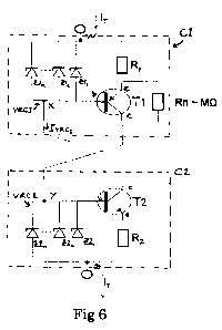
Figure 6 shows a two-terminal current regulator circuit
according to a first embodiment of the present invention, the
current regulator circuit having a first current regulator
circuit 01 cross-coupled to a second current regulator circuit
C2. The first current regulator circuit Cl comprises a driver
circuit having a resistor R1 and a bipolar transistor Ti. The
first current regulator circuit also comprises a voltage
regulator circuit VRC1 comprising a plurality of Zener diodes
Zil, Z1... Zlõ connected in parallel. The second current regulator
circuit C2 comprises a driver circuit having a resistor R2 and
a bipolar transistor T2. The second current regulator circuit
also comprises a voltage regulator circuit VRC2 comprising a
plurality of Zener diodes Z21, Z22_ Z2n connected in parallel.
17
CA 02840369 2013-12-23
WO 2013/005002 PCT/GB2012/051448
A voltage source drives a current IT into node W which connects
resistor R1 and the positive terminal of the voltage regulator
circuit VRC1 of the first current regulator circuit Cl such that
the current IT is divided between the resistor R1 and VRC1. The
resistor R1 is connected to the emitter e of transistor Ti. The
collector current of the bipolar transistor Ti, which is
determined by the value of R1, the voltage produced by the VRC1
and by the base-emitter voltage Vbe of the transistor Ti, is
supplied to the positive terminal of the voltage regulator
circuit VRC2 of the second current regulator circuit C2 and to
the base of transistor T2 at node Y. Node X connects the negative
terminal of VRC1, the base of Ti and the collector of T2. Resistor,
Rn is simply a source of thermal noise, used to 'kick-start'
the circuit.
Assuming negligible base current at T2, IvRin is equal to the
collector current of T2. Furthermore, the collector current of
T2 is determined by the value of R2, the voltage produced by
the VRC2 and by the base-emitter voltage vbe of transistor T2.
The negative terminal of VRC2 is connected to R2 forming the
output node Z through which IT flows to the intended load.
By virtue of the cross-coupling of this circuit, the two
transistors are advantageously provided with base-biasing
currents.
According to the above embodiment, one of the resistors may be
held at a constant value, whilst the other is used as a current
programming resistor. Alternatively, both of the resistors may
be variable in order that they both serve as current programming
resistors.
According to a second embodiment of the present invention shown
18
CA 02840369 2013-12-23
WO 2013/005002 PCT/GB2012/051448
in Figure 7, a current regulator circuit Cl is connected to a
resistive summing circuit RSC. The person skilled in the art
will appreciate that various designs for the resistive summing
circuit are possible. For example, in the particular example
shown in Figure 7, the resistive summing circuit comprises
a plurality of resistors connected in parallel.
The following describes the properties and principles of
preferred embodiments of the present invention.
Setting accuracy: The 'setting accuracy' of a current regulator
according to embodiments of the present invention is discussed
herein, in terms of the variations in the current provided by
such a regulator, caused by random variations in the properties
of circuit elements. Whilst it should be appreciated by the
reader that both random errors and deterministic errors occur
in any circuit, it is the random errors that give rise to spreads
in circuit performance. Deterministic errors give rise to fixed
'offsets' between designed and realised performance. The
setting accuracy of any constant current circuit is properly
expressed as the fractional change in regulated current. Thus,
for a circuit according to the general topology of figure 3:
A/T/Ii = (A Vreg + Avbe)/(Vreg - vbe) equation 6
Wherein, LVreg is the manufacturing spread in Vreg and Avbe is
the manufacturing spread in vbe. In the present invention, the
regulating voltage Vreg is provided by low-voltage Zener diodes
and therefore, ,6Vreg = LVz . This spread in Vreg is significantly
greater (by a factor of around 10) than the spread in vbe.
Therefore:
19
CA 02840369 2013-12-23
WO 2013/005002 PCT/GB2012/051448
MT/h, ilVz/(Vreg ¨ vbe) equation 7
Typically, for a low voltage (<5.5 Volts) Zener diode, LVz, the
statistical spread in Zener voltage is around 10% - equating
to a spread of +/- 5% in Vz. Eqn 6 indicates that the use of
low voltage Zener diodes would, in the absence of any correction
means, give rise to a large variation in IT with manufacturing
tolerance in Vz - in other words, a poor current setting accuracy.
It therefore becomes desirable, in accordance with embodiments
of the present invention, to combine Zener diodes in such a way
as to ameliorate this effect.
According to embodiments of the present invention, use is made
of a statistical theorem, known as the Central Limit Theorem.
One consequence of this theorem is that if a variable, x, is
distributed according to a normal distribution, with mean, p
and standard deviation, a, then the mean of samples of size N,
will be distributed according to a normal distribution, with
the same mean, p and a standard deviation of
Consider the case of a Zener diode, with a nominal Zener voltage,
Vz and a manufacturing tolerance, LVz. The value of LVz will
be related to the standard deviation a (Vz) of the wafer-to-wafer
statistics of Vz. Typically, the value quoted for the
manufacturing spread in Vz will be around +/- 3. a (Vz) - the
'six sigma spread' .
If samples of N Zener diodes are taken from this 'global'
distribution, to form each parallel diode stack, then the mean
value of Zener voltage, <Vz> within each sample will have a mean
value, <(<Vz>)> equal to the nominal Zener voltage, Vz and a
standard deviation of a (Vz) /VN.
CA 02840369 2013-12-23
WO 2013/005002 PCT/GB2012/051448
According to embodiments of the present invention which use a
Voltage Regulation Circuit, VRC, the/each VRC is provided which
comprises a parallel stack of Zener diodes, each with the same
nominal Zener voltage, Vz.
The regulator, having two diode stacks, carrying currents Isi
and Is2 has a total regulated current, IT given by:
IT= Is( + Is2 equation 8
Thus
IT = f(<VZ2> - Vbe) + (<VZ1> - vbe)I/R equation 9
The variance in this total current is given by:
Var(IT)= (Var(<Vz2>)+ Var(Vzi>)/R2 equation 10
From the Central Limit Theorem:
Var(<Vz2>) = Var(<Vzi>) = Var(Vz)/N equation 11
Therefore:
Var(IT)= 2.Var(Vz)/(N.R2) equation 12
It can be shown that the nominal regulated current, 'mom, through
the regulator is given by:
/Thom =2. (Vz - vbe)/R equation (13)
Wherein, Vz takes its nominal value as quoted in the
manufacturer's datasheet.
The standard deviation in IT is given by:
o-(h) = SqrtVar(IT)= Sqrt(2/N.R2).cr(Vz) equation 14
21
CA 02840369 2013-12-23
WO 2013/005002
PCT/GB2012/051448
The 'Setting Accuracy' of IT is given by the spread in TT (LIT)
as a fraction of ITnom, where the spread is 6. a (IT) . Similarly,
the manufacturing spread in Vz (AVz) is equal to 6. a (Vz).
Therefore:
A(IT) = Sqrt(2/NR2).A(Vz)
equation 15
A(IT)/ITnom = Sqrt(2/NR2).A(Vz)/IT,nom equation 16
AO-WI-rum = A(Vz)/[Sqrt(2.N).(Vz ¨ vbe)]
equation 17
Wherein, N is the number of Zener diodes in each stack. Therefore,
this fractional error in regulator current, for a regulator
according to the present invention reduces with the number of
Zener diodes per stack, by a factor Sqrt (2.N) .
Temperature coefficient and current programming range: The
temperature coefficient of current for a regulator embodying
the present invention is given by:
TC = (gVz/87.- ovbe/gT)/(Vz - vbe)
equation 18
This temperature coefficient is substantially zero when the
current through each Zener diode is equal to Iz, opt (the value
of Zener current at which oVz/5T = ovbe/oT) . Consequently, there
are values of regulator current, IT, at which TC is substantially
zero. For optimal thermal performance, therefore, these values
of IT become `preferred' operational currents for a regulator
embodying the present invention.
As the Zener current, Iz, departs from this optimal value, the
22
CA 02840369 2013-12-23
WO 2013/005002
PCT/GB2012/051448
value of TC changes. Preferred embodiments of the present
invention seek to provide a current programming range over which
TC deviates from zero by only a small amount. For illustrative
purposes, we shall take this current programming range as being
that over which the value of TC is bounded within the range +/-
75 ppm per Kelvin. Therefore, in defining upper and lower
bounded values of temperature coefficient, TO, as TCG = 7.5x10⁵
per K and TCL = -7 .5x10-5 per K, the upper and lower values of
oVz/6T corresponding to the two ends of the current programming
range are:
(57/z/g1)L = TCL.(Vzif - vbe) + gvbe/6T equation 19
and
(gVz/8T)u = TCu.(Va- vbe) + 8vbethT equation 20
TCG is the upper bound value of TO, which corresponds to the
lower bound of Zener current; TCL is the lower bound of TO, which
corresponds to the upper bound of Zener current. Vzu and VzL
denote the values of Zener voltage at the upper and lower limits
of Zener current respectively. These values of Vz can be
accurately approximated by assuming, a-priori, that the range
of current through the mean Zener diode within each stack is
around 10mA to 20mA. This range of currents is centered on a
value of Zener current that corresponds to the value of Iz, opt
for a 2.4V Zener diode, chosen for reasons given later. Then
the accurate values of Iz (Iz,G and Iz,L) corresponding to the
lower and upper values of 6Vz/6T respectively, can usually be
obtained from the Zener diode manufacturer's datasheet. The
corresponding values of IT are then:
= 2.IV.Iz,u and IT,L = 2.N.1Z,L
equation 21
Assuming the bipolar transistors have high values of p(Ic/Ib)
23
CA 02840369 2013-12-23
WO 2013/005002 PCT/GB2012/051448
the total current through the regulator at the centre of its
programming range, for a given value of N is given by:
IT,cen = 2.N.Iz,opt equation 22
From equation 9, the value of the programming resistor
corresponding to this central value of current is given by:
R =2.(Vz> - vbe)trixen equation 23
Where the <Vz> takes the value of the nominal Zener voltage at
Iz, opt. For values of total regulator current elsewhere within
the programming range:
R =2.(<Vz> - vbe)/17, equation 24
Current sharing: It is known in the art that difficulties arise
in connecting Zener diodes in parallel. These difficulties
relate to the extent to which Zener diodes share current -
similar to the case of bandgap reference diodes used in the prior
art depicted in figure 4. If the differential Zener impedance
(rate of change of Zener voltage, Vz, with current) at around
the operating current per Zener diode (Iz, opt) is
insufficiently high, or if the manufacturing spread in Vz (Vz)
is too high, then the Zener diode with the lowest Zener voltage
in the stack will take all (or at least most) of the current.
To counter this problem, thereby ensuring that all the Zeners
in each stack get turned on, it is preferable to use Zener diodes
with a small manufacturing spread in Zener voltage and a nominal
Zener voltage for which the Zener impedance at I z, opt is greater
than a few Ohms. Thus, according to preferred embodiments, a
small variation exists between the Zener voltages of the Zener
diodes. The differential Zener impedance is normally regarded
24
CA 02840369 2013-12-23
WO 2013/005002
PCT/GB2012/051448
as a 'parasitic' or unwanted impedance. However, in the context
of the present invention this usefully facilitates current
sharing.
This is shown by reference to figure 8, which depicts the I/V
characteristics of two Zener diodes, Zl and Z2, with Zener
voltages lying at the extremities of the manufacturing
tolerance range for a given nominal Zener voltage. The Zener
voltage of each Zener diode is defined, in accordance with the
definition of the nominal Zener voltage, as the voltage across
the diode at a defined diode current, of normally 5mA.
Furthermore, in view of the design of the regulator using such
Zener diodes, whereby the nominal Zener current is Iz,opt, the
currents through Zener 1 and Zener 2 in figure 6, lie either
side of this value. Therefore, by construction, the
relationship between (Iz1 - Iz2) and (Vz2 - Vzi) is given by:
(!z/ - /z2) = (Vz2 - Vzi)/Rz
equation 24
Wherein, Rz is the Zener resistance (the real part of the Zener
impedence, Z2) at Iz,opt. For a typical 2.4 Volt Silicon Zener
diode (cited for reasons given later) Rz is around 35Q and Iz,opt
is substantially 14.5mA. The manufacturing spread in Vz (Vz2
-Vzi) is typically 0.24V. Therefore, the worst-case difference
in the currents through Zener 1 and Zener 2 is around 7mA. This
means that Zener 1 carries a current of Iz,opt plus 3.5mA (Iz1
= 18mA) whilst Zener 2 carries a current of Iz,opt minus 3.5m7
(Iz2= 11m) . By inspection of the thermal behaviour of atypical
2.4 Volt Silicon Zener diode, the typical rates of change of
Vzi and Vz2 with temperature are (at 18mA and 11rnA respectively)
substantially -2.1 mV/K and -1.9 mV/K. Therefore, the average
rate of change of Zener voltage with temperature is
CA 02840369 2013-12-23
WO 2013/005002 PCT/GB2012/051448
substantially -2.0 mV/K, as desired for optimal thermal
behaviour (oVz/5T = 5vbe/6T) at a nominal current per Zener
diode of Iz, opt .
Therefore, in contrast to a circuit using combinations of
forward-based PN junction diodes and bandgap reference diodes,
a circuit embodying the present invention advantageously uses
current-sharing voltage references (low voltage Zener diodes)
within each VRD. In view of the fact that, in contrast to bandgap
reference diodes, such low-voltage Zener diodes are simple PN
junction structures, this provides a cost-effective means by
which the current handling capabilities and therefore, the
current programming range of a current regulator can be selected,
according to the number of such low-voltage Zener diodes used
in each VRD.
The utility of this approach is shown by reference to a series
of different embodiments, each differing in terms of the number
of Zener diodes per VRD.
The preferred selection criteria for Zener diodes used in a
preferred embodiment of the present invention are, in light of
the preceding:
1. AVz (manufacturing spread in Vz - i.e. the variations
arising between the Zener voltages of the plurality of
Zener diodes comprised in a given VRD) should be low. This
advantageously ensures good setting accuracy and
facilitates current sharing.
2. The Zener impedence Zz should be high at operating current
per diode, Iz, opt in order to advantageously enable
current sharing.
26
CA 02840369 2013-12-23
WO 2013/005002 PCT/GB2012/051448
3. Vz at Iz, opt should be low in order to achieve a low
'drop-out voltage', which is equal to 2xVz .
4. The rate of change of 5Vzi5T with current (6Vz,t5T.5Iz)
should be low, for currents around Iz, opt in order to
advantageously achieve a wide programmable current range.
5. The value of Iz, opt should be low for cases where the
setting accuracy of programmed current is particularly
important, as this forces N to be high for any given value
of regulator current
Inspection of thermal performance data for several commercially
available Silicon Zener diodes shows that the first four of
these criteria are substantially met by choosing a Zener diode
with a low Zener voltage or, preferably the lowest available
Zener voltage - typically, 2.4V at the Zener voltage reference
current, 5mA. For applications in which setting accuracy of
programmed current is particularly important, a slightly higher
Zener voltage (substantially 3.0V at 5mA) can be chosen, as this
is consistent with a lower value of Iz, opt, consistent with
preferred selection criterion 5.
Example embodiments:
For a typical 2.4V Silicon Zener diode, where the Zener voltage
is measured at a Zener current of 5mA, the Zener voltage at Tz, opt
(which is substantially 14.5mA) is 2 . 9V. Also, for a typical
NPN or PNP Silicon transistor, carrying an appreciable emitter
current, vbe .-- 0.7V.
LVz = 0.24 V
I z , opt = 14.5 mA
Zz @ Iz,opt = 35 Q
27
CA 02840369 2013-12-23
WO 2013/005002
PCT/GB2012/051448
Vz @ Iz,opt = 2.9 V
Vz @ 10mA (value taken for VzL) = 2.75 V
Vz @ 20mA (value taken for Vz) = 3.1 V
(c5Vz/6T)u = - 1.85 mV/K
(6Vz/6T)L = - 2.18 mV/K
= 9.5 mA, = 23.5 mA
Performance metrics can be calculated from these figures,
assuming the resistors (R) have zero temperature coefficient.
In practice, ultra-low temperature coefficient resistors
represent a significant uplift in cost. Affordable thick-film
chip resistors, however, are currently available, with
temperature coefficients of -1+-25 ppm/K across the resistance
range required and with resistance accuracies of +/-0.1%. The
performance metrics for a range of N from 1 to 6 are given in
Table 1.
Centre R @ Setting Programmable
Current Range,
Current IT,õõ, Accuracy over which
/T,cen OW (0) of -
75ppm/K < TC < +75ppm/K
(at which, current IT,L ITJJ (mA)
TC = 0) @ IT , cen
1 29 151.7 +/- 19 47
55 %
.
2 58 75.86 +/- 3.9% 38 94
3 87 50.57 +/- 3.2 % 57 141
4 116 37.93 +/- 2.7 % 78 188
5 145 30.34 +/- 2.4 % 97 235
6 174 25.29 +/- 2.2 % 116 282
/0 TABLE 1
This shows that embodiments of the present invention
advantageously provide a topology for a current regulator,
based on which, regulators can be designed which provide a range
of programmed currents from around 20 mA to around 280 mA, over
28
CA 02840369 2013-12-23
WO 2013/005002
PCT/GB2012/051448
which a temperature coefficient of current, lying between - 75
ppm per Kelvin and + 75 ppm per Kelvin (- 0.0075 % per Kelvin
and + 0.0075 % per Kelvin) is maintained. Each embodiment of
the present invention comprises two bipolar Silicon transistors
and a number of low-voltage Silicon Zener diodes, beneficially
providing a low-cost solution.
Manufacturing variations in the value of Iz,opt would be
sensibly accommodated by specifying a product designed
according to a particular embodiment of the present invention,
over a narrower programmed current range. A realistic range of
currents over which the +/- 75 ppm per Kelvin temperature
coefficient can be specified would be around 25 mA to 220 mA.
In circumstances where low drop-out voltage and therefore low
Zener voltage, is less important than setting accuracy, it would
be advantageous to use Zener diodes having a slightly higher
Zener voltage, consistent with the need to maintain high Zener
impedance. Such slightly higher voltage (e.g. 3.0V) Zener
diodes have lower values of Iz,opt. This means that for any given
regulator current, a higher number of Zeners would be required
in each stack, leading, in view of the Central Limit Theorem,
to a greater setting accuracy for that regulator current.
In circumstances where the value of TC is required to be
substantially zero at a specific current, 'spec, or over a small
range of programmed currents centred on 'spec, it is possible
to choose a value of Zener voltage for which Silicon Zener diodes
have a value of Iz,opt given by:
Iz,opt = '3pec/2.N
equation 25
Where N is an integer and corresponds to the number of Zener
diodes per VRD in such a regulator circuit.
29
CA 02840369 2013-12-23
WO 2013/005002 PCT/GB2012/051448
For example, it can be shown that for Vz = 2 . 7 V. the
corresponding value of Iz, opt for a Silicon Zener diode is
typically 5 mA. Therefore, it is possible to construct a current
regulator circuit, embodying the present invention, which uses
two such Zener diodes per VRID and which has a temperature
coefficient of current, TO, which is substantially equal to zero
for a total regulator current, IT, of 20 mA.
Furthermore, in order to facilitate ease of current programming,
a regulator embodying the present invention could be used, where
one of the programming resistors is held constant (at the centre
current value, for a given N) whilst the other is used as the
programming resistor.
30