Note: Descriptions are shown in the official language in which they were submitted.
Optoelectronic module comprising a lens system
Technical Field
The invention relates to an optoelectronic module, an optoelectronic device, a
method for
manufacturing an optoelectronic module, as well as a use of an optoelectronic
module. Such
optoelectronic modules, optoelectronic devices, methods and uses can be
employed in natural
sciences, technology, medicine and daily life in various manners. An important
field of
application to which the invention, however, is not limited, is its use in the
field of process
technology, for example, for the purpose of drying and/or hardening materials
and/or objects or
for the purpose of a photochemical modification of workpieces. As an
alternative or in addition,
optoelectronic modules and optoelectronic devices of the type described below
can, for
example, also be used in the field of illumination, for example, in traffic
engineering and/or in
building services.
Background
In particular, the invention relates to optoelectronic modules which are
designed as what are
called chip-on-board modules, either as a whole or in part. Such chip-on-board
modules are
modules which can be manufactured according to what is called chip-on-board
technology
(CoB), either as a whole or in part. According to chip-on-board technology,
one or more
unhoused semiconductor components (semiconductor chips) are directly mounted
to a
substrate, for example, a printed circuit board or another type of
interconnect devices. In
general, the term of chip-on-board module therefore relates to an electronic
assembly which
includes at least one substrate as well as at least one unhoused (naked)
semiconductor
component mounted to a substrate. For example, such chip-on-board modules are
used as
luminous elements, as high-performance lamps (for example, as high-performance
UV LED
lamps), as photovoltaic modules, as sensors, or in any other manner. In
particular, the
optoelectronic modules suggested are optoelectronic chip-on-board modules
having a plurality
of optoelectronic components. Within the scope of the present invention, the
optoelectronic
components used therein may, for example, however not exclusively, be light-
emitting diodes
(LEDs) and/or photodiodes, particularly in the form of chips or other
components, which are
arranged in the chip-on-board module on a planar substrate, more particularly
a substrate made
of metal, ceramic or silicon, a metal-core or FR4 printed circuit board, a
glass substrate, a
plastic substrate, a metal matrix compound material, or similar substrates.
These chip-on-board
modules must be protected against mechanical damage and corrosion. To achieve
this, it is
tried to find solutions that are as compact and simple as possible.
CA 2842117 2018-08-20
CA 02842117 2014-01-16
=
2
Since, usually, protection in the form of housings on chip-on-board modules is
complex in terms
of costs and technology, planar potting of all or a plurality of components
with a plastic-based
potting material is known as practical prior-art alternative for protecting
such chip-on-board mod-
ules. Along with other functional components, such as solder tracks and
contacting elements, the
optoelectronic components in chip-on-board modules, together with a planar
substrate, can be
protected against mechanical damage and corrosion by means of coatings.
Furthermore, a directivity of the optoelectronic modules plays an important
role for many applica-
tions. For optoelectronic components, directivity generally describes an
angular dependence of
the strength of waves received or transmitted, which is usually related to a
sensitivity and/or in-
tensity in a main direction, i.e., along an optical axis of the optoelectronic
components. In particu-
lar, a radiation intensity and/or a directional characteristic of the
optoelectronic module usually
play an important role in optoelectronic modules which comprise one or more
light-emitting di-
odes as optoelectronic components. This directional characteristic is a
special from of the direc-
tivity and, in this case, describes the angular dependence of the
electromagnetic field and/or the
intensity of the electromagnetic waves emitted, more particularly in the form
of infrared, ultraviolet
or visible light. Chip-on-board modules are to advantage in that light-
emitting diodes can be ap-
plied onto the substrate with a high packaging density, this increasing the
radiation intensity. In
many cases, however, an additional optical system is used to affect the
directional characteristic
of the optoelectronic modules. For light-emitting optoelectronic modules as
well as for photosen-
sitive optoelectronic modules, this optical system can, for example, be lens
systems comprising
one or more lenses, more particularly what are called microlens systems. For
example, the lens
systems, more particularly the microlens systems, can comprise one or more
beam-forming ele-
ments the lateral extension of which, for example the extension of which in a
plane of the sub-
strate, may range from the sub-millimetre range to the decimetre range or even
to the metre
range. For example, the microlens systems can be designed such that these
optically active
ranges comprise structures in the sub-millimetre range, for example,
structures having a diffract-
ing, scattering, converging, collimating or diffusing effect.
Due to the fact that the distances required between the optoelectronic
components are usually
short, more particularly due to the short pitch (centre-to-centre distance
between neighbouring
optoelectronic components) typically used in chip-on-board modules, there are
only a few known
CA 02842117 2014-01-16
3
methods allowing the implementation of beam-forming microlenses above the
individual optoelec-
tronic components, for example, the individual light-emitting diodes of an
array of light-emitting
diodes, for example by means of an appropriate potting material.
For example, the post-published document, DE 10 2010 044 470, from the house
of the Applicant
of the present application describes a method for coating an optoelectronic
chip-on-board module
which comprises a planar substrate fitted with one or more optoelectronic
components. Therein,
use is made of a transparent UV- and temperature-resistant coating consisting
of one or more
silicones. According to the method, the substrate to be coated is pre-heated
to a first tempera-
ture. Furthermore, a bank is applied which encloses an area or partial area to
be coated of the
substrate. This bank, as a whole or in part, is composed of a first thermally
hardening, highly re-
active silicone which hardens at a first temperature. This first silicone is
applied to the pre-heated
substrate. Furthermore, the area or partial area of the substrate that is
enclosed by the bank is
filled with a liquid second silicone, and the second silicone is hardened.
Therein, it is also possi-
ble to apply quickly hardening lenses onto individual components of the
substrate, particularly by
means of the first silicone. In this manner, it is also possible to form
microlens systems.
Furthermore, a coating method for an optoelectronic chip-on-board module is
known from the
likewise post-published document, DE 10 2010 044 471, that is also originating
from the house of
the Applicant of the present application. Again, the optoelectronic chip-on-
board module com-
prises a planar substrate which is fitted with one or more optoelectronic
components and includes
a transparent UV- and temperature-resistant coating consisting of silicone.
The method com-
prises a method step of potting a liquid silicone into a mould that is open at
the top and comprises
outside dimensions that correspond to the outside dimensions of the substrate
or are in excess
thereof. Furthermore, the substrate is introduced into the mould wherein the
optoelectronic com-
ponent or the optoelectronic components completely immerse(s) into the
silicone. In a further
method step, the silicone is hardened and cross-linked with the optoelectronic
components and
the substrate. Furthermore, the substrate provided with the coating consisting
of the hardened
silicone is removed from the mould.
Furthermore, an LED array which comprises a lens array for converging
divergent light from each
LED is known from US 7,819,550 B2. The lenses each comprise a flat section and
two curved
sections. The lenses are not curved above the light-emitting diodes.
4
A method for manufacturing a white-light LED is known from US 2007/0045761 Al.
Therein,
use is made of an LED which emits blue light and use is made of phosphoruses
which convert
the light. Among other things, said document also describes the moulding of
optical systems
above the light-emitting diodes, which are produced by means of a casting
process that is
sealing against the atmosphere.
Furthermore, a method for encapsulating light-emitting diodes by means of a
compressing
casting method is known from US 2010/0065983 Al. Therein, use is made of a
tape for sealing
during the casting process.
Despite the improvements described above and achieved for known optoelectronic
modules,
there is still a demand for optoelectronic modules with improved directivity,
more particularly a
demand for optoelectronic modules with a high radiation intensity for specific
applications. In
particular, there is a demand for efficient light sources that can be mounted
side by side and the
lighting profile of which may have a high radiation intensity at an adjustable
distance, wherein
high homogeneity requirements are met at the same time and a sufficiently
steep drop can be
registered in the edge region. Such optoelectronic modules, more particularly
modules of light-
emitting diodes, are required for lithographic applications in the industrial
production of the
printing industry in order to reach a uniform and high-quality drying image of
print colours and
inks. High radiation intensities, for example, generally radiation intensities
of more than 100
mW/cm2, typically 1-20 W/cm2, up to a few 100 W/cm2, are usually required for
reaching high
process velocities with light sources that are as compact and energy-efficient
as possible.
Summary
It is therefore the object of the present invention to provide an
optoelectronic module which
obviates the drawbacks of known methods at least to a large extent and which
meets the
aforementioned requirements at least to a large extent. In particular, it is
the object of the
present invention to provide an optoelectronic module which, when configured
as a light-
emitting module, comprises a high efficiency and radiation intensity, which
can be used as a
side-by-side-mounting light source, and which comprises a lighting profile
having a high
homogeneity and a sufficiently steep drop in an edge region.
CA 2842117 2018-08-20
5
This problem is solved by an optoelectronic module, an optoelectronic device,
a method, and a
use. In accordance with one aspect of the present invention there is provided
an optoelectronic
module (112), specifically an optoelectronic chip-on-board module (114),
wherein the
optoelectronic module (112) comprises a substrate (116), wherein the substrate
(116) has a
planar design, furthermore comprising a plurality of optoelectronic components
(118) that are
arranged on the substrate (116), wherein the optoelectronic module (112)
furthermore
comprises a lens system (122) having a plurality of lenses (124), wherein the
optoelectronic
components (118) are arranged on the substrate (116) in a one-dimensional or
two-dimensional
array characterised in that the lens system (122) comprises at least two
lenses (124) with
different directivities wherein the at least two lenses (124) with different
directivities comprise
lenses (124) with different heights, wherein the lens system can comprise a
stepwise change in
the directivities, the directivities continuously or discontinuously change
from an interior region
of the lens system towards an edge of the lens system, wherein at least one
lens (124) of the
lens system (122) comprises a surface curvature with at least one convex area
and at least one
concave area, wherein the convex and concave areas are arranged on a side of
the lens
system facing away from the substrate.
An optoelectronic module is suggested according to a first aspect of the
present invention. In
general, an optoelectronic module is to be understood as an assembly which can
be handled as
a unit and which comprises at least one optoelectronic component, for example,
a light-emitting
electronic component and/or a light-sensitive electronic component. The
optoelectronic module
can, in particular, be designed as an optoelectronic chip-on-board module
according to the
definition mentioned above.
The optoelectronic module comprises a substrate that has a planar design.
Within the general
scope of the present invention, a substrate is to be understood as an element
that is established
to receive one or more electronic, more particularly one or more
optoelectronic, components. In
particular, the substrate can be designed according to the type described
above with regard to
the state of the art and can comprise one or more interconnect devices, more
particularly
according to the type mentioned. A planar design is to be understood as a
design in which at
least one surface that can be fitted with the optoelectronic component, more
particularly an
unhoused chip, for example a flat or a slightly curved surface onto which one
or more
optoelectronic components, more particularly one or more optoelectronic chips
without housing,
can be applied.
CA 2842117 2018-08-20
5a
For example, the planar substrate can be designed flat as a whole or in part,
for example, as a
printed circuit board.
Furthermore, the optoelectronic module comprises a plurality of optoelectronic
components that
are arranged on the substrate. In particular, these optoelectronic components
can be arranged
on the substrate in chip-on-board technology. Optoelectronic components, as
described above,
are to be understood as components which fulfill at least one optoelectronic
function, for
example, a light-emitting and/or light-sensitive function. In particular, the
optoelectronic
components can be selected from the group consisting of light-emitting diodes
and photodiodes.
The optoelectronic components can, in particular, comprise one or more
unhoused chips.
Accordingly, the plurality of optoelectronic components can, in particular,
comprise an array of
optoelectronic components, i.e., an arrangement in which a plurality of
optoelectronic
components are applied onto the substrate in one or more rows. For example,
the array can
comprise a rectangular matrix with at least
CA 2842117 2018-08-20
CA 02842117 2014-01-16
6
one row and/or at least one column or with a plurality of rows and columns.
Therein, a row and/or
column is to be understood as a linear arrangement of at least two,
preferrably at least three, four
or more optoelectronic components. That means that the plurality of
optoelectronic components
can, preferrably, comprise a rectangular matrix of light-emitting diodes
and/or photodiodes. As a
matter of principle, however, other embodiments are also possible, for
example, embodiments in
which the plurality of optoelectronic components is irregularly arranged on
the substrate and/or is
arranged on the substrate in a non-rectangular matrix.
Furthermore, the optoelectronic module comprises a lens system, more
particularly a microlens
system, having a plurality of lenses, more particularly microlenses. Therein,
a lens is generally to
be understood as an optical element which is able to form electromagnetic
beams wherein the
electromagnetic beams are diffracted at least once. Therein, lenses, for
example microlenses,
can comprise lateral dimensions from the sub-millimetre range to the metre
range. For example,
lamp systems for industrial applications can comprise lateral extensions, for
example lengths, of
up to 3 m or more. In particular, the lenses can comprise converging and/or
scattering properties.
A lens system, more particularly a microlens system, is to be understood as a
plurality of lenses,
more particularly microlenses, which are preferrably arranged next to each
other, for example in a
plane parallel to a plane of the planar substrate. For example, the lens
system can comprise an
array of lenses, wherein a plurality of lenses is arranged in one or more rows
and/or one or more
columns. For example, the lens array can, in turn, comprise a rectangular
array. As will be ex-
plained in more detail below, one lens can, for example, each be assigned to
exactly one opto-
electronic component or a group of a plurality of optoelectronic components,
with the result that
the lens system can, for example, be arranged in an array that can correspond
to the array of the
optoelectronic components. In particular, the lens system can, as a whole or
in part, be made of a
continuously designed optically transparent material that forms a plurality or
all of the lenses of
the lens system. This optically transparent material, for example a plastic
material, can particu-
larly be directly applied onto the optoelectronic components, for example in a
casting process.
For example, the lens system can generally comprise an optically transparent
material that is in
contact with the optoelectronic components and that forms the plurality of
lenses or at least a
plurality of lenses of the lens system.
The lens system comprises at least two lenses, for example at least two
microlenses having a
different directivity. As has been mentioned above, directivity is, therein,
to be understood within
CA 02842117 2014-01-16
7
the general scope of the present invention as an angular dependence of
received or transmitted
electromagnetic waves, more particularly light in the visible and/or infrared
and/or ultraviolet
spectral range. For example, this angular dependence can refer to the
electromagnetic field of
the electromagnetic waves. As an alternative or in addition, the angular
dependence can, for ex-
ample, also refer to an intensity and/or an energy density and/or another
physical variable char-
acterising the strength of the electromagnetic waves. For example, the
directivity can be specified
with reference to a strength in a main direction which is, for example,
parallel to an optical axis of
the optoelectronic component, for example an axis which drives through a
sensitive and/or emit-
ting active surface of the optoelectronic component in a vertical and centric
manner. In particular,
the directivity can comprise a directional characteristic if the
optoelectronic module comprises
one or more optoelectronic components in the form of light-emitting
components, for example
light-emitting diodes. For example, the directional characteristic can be
measured by means of an
appropriate sensor which is arranged at a variable angle and at a
predetermined distance in front
of the optoelectronic component, wherein continuous or discontinuous
measurements of a
strength of an emission, for example, measurements of an intensity, are taken
at different angles.
In this manner, it is, for example, possible to register directivities by
means of appropriate polar
diagrams of the measurements. Such measuring methods are known to persons
skilled in the art
from the field of lighting technology. As a matter of principle, the precise
embodiment of the
method used is, therein, of no importance for the present invention because
nothing but a com-
parison of the directivities of the lenses is made.
The directivity of a lens can, in particular, be understood as the directivity
of a lens in cooperation
with an optoelectronic component, for example a light-emitting diode, that is
assigned to the lens.
As has been described above, the lenses can, in particular, each be assigned
to one optoelec-
tronic component of the plurality of optoelectronic components, with the
result that, for example,
exactly one lens of the lens system is arranged above each optoelectronic
component. Accord-
ingly, a directivity of the lens is then to be understood as the directivity
of the group that is com-
posed of the optoelectronic component as well as the lens arranged above that
optoelectronic
component.
The directivities of the at least two lenses can differ from each other, for
example, with regard to
an opening angle, for example with regard to an emission angle. For example,
an emission angle
can be understood as an angle which is enclosed by the lateral points with
half of the maximum
CA 02842117 2014-01-16
8
light intensity. It is, however, also possible to use other characteristics of
the directivity for com-
paring the directivities.
For example, the at least two lenses the directivities of which differ from
each other can be ar-
ranged in an interior region of the lens system, for example of the lens
array, and at an edge of
the lens system, for example of the lens array. For example, the lens system
can comprise a lens
array in the form of a one-dimensional or a two-dimensional matrix of lenses.
For example,
lenses that are arranged at an edge of the lens array can, therein, comprise a
different directivity
than lenses that are arranged in the interior region of the lens array. In the
case of a linear matrix,
this edge can, for example, each consist of the outermost lenses. In the case
of a two-
dimensional matrix, the edge can comprise a line or a frame of lenses which
are arranged at the
edge of the lens system. These edges can differ from at least one lens which
is arranged in the
interior region of the lens system, i.e. aside the edge, with regard to their
directivities. Therein, the
lenses of the lens system can be designed such that at least two groups of
lenses are provided,
wherein the lenses of at least one first group comprise a first directivity
and wherein the lenses of
the at least one second group comprise at least one second directivity,
wherein the first directivity
and the second directivity differ from each other. Therein, the lens system
can comprise a step-
wise change in the directivities, with the result that, for example, the
directivities continuously or
discontinuously change from an interior region of the lens system towards an
edge of the lens
system. Therein, two or more steps of the change can be provided.
As has been mentioned above, the optoelectronic components can be arranged on
a substrate in
a one-dimensional or two-dimensional array, i.e. in a one-dimensional or two-
dimensional matrix.
In particular, this array can comprise a line or a two-dimensional matrix
wherein, in a two-
dimensional matrix, at least two optoelectronic components are arranged in
each of two dimen-
sions. In particular, the one-dimensional or two-dimensional array can
comprise a number of at
least 2, at least 4, at least 8, at least 10, at least 50, or even at least
100 of optoelectronic com-
ponents. Therein, an even number of optoelectronic components or an uneven
number of opto-
electronic components is conceivable because it is, for example, even possible
to implement ar-
rangements in an array that deviate from rectangular grid arrangements, for
example hexagonal
arrangements of the optoelectronic components in the array, for example
hexagonal LED arrays.
CA 02842117 2014-01-16
9
As has been mentioned above, the optoelectronic components can, in particular,
be selected
from the group consisting of light-emitting diodes, more particularly surface-
emitting light-emitting
diodes, and photodiodes.
The at least two lenses with different directivities can, in particular,
comprise lenses with a differ-
ent surface curvature. Therein, a surface curvature is generally to be
understood as a design of
the surface in one or more cutting planes through the lens, for example a
cutting plane which
extends through an optical axis of the optoelectronic component and/or the
lens, which is also
referred to as main direction. The lenses can be designed such that they are
rotationally symmet-
rical around this optical axis or they can also be designed asymmetrically. A
convex curvature
can, for example, describe an area having a converging effect, and a concave
curvature can, for
example, describe an area having a scattering effect.
As an alternative or in addition to lenses with different surface curvatures,
the at least two lenses
with different directivities can also comprise lenses with different heights.
Therein, a height is to
be understood as a distance between an outermost surface of the lens and an
active surface of
the electrical component which is assigned to the lens. For example, this
distance can be meas-
ured along an optical axis vertically to the substrate and/or vertically to
this active surface.
As an alternative or in addition to the embodiments described above, the at
least two lenses with
different directivities can also comprise lenses with different base areas.
Therein, a base area is
to be understood as the shape and/or the size of the lens in a cutting plane
which is positioned in
the plane of an active surface of the optoelectronic component which is
assigned to the lens. This
plane can coincide with a plane of the substrate or can also be arranged
offset to this plane of the
substrate.
As an alternative or in addition to one or more of the aforementioned
possibilities, the at least two
lenses with different directivities can also comprise lenses in which an
optical axis of each lens is
aligned in a different manner with an optical axis of each optoelectronic
component. As has been
described above, one lens each can be assigned to exactly one optoelectronic
component or also
a plurality of optoelectronic components. The lens can comprise an optical
axis, and the assigned
optoelectronic component can also comprise an optical axis. Therein, use can
be made of a ra-
dially symmetric structure in which the optical axes of the lens and the
assigned optoelectronic
CA 02842117 2014-01-16
component coincide. It is, however, also possible to provide a different
alignment, for example, an
alignment in which the optical axes of the lens and the assigned
optoelectronic components are
offset from each other in parallel. As an alternative or in addition, the
optical axis of the lens and
the optical axis of the optoelectronic component can also be aligned with each
other in a slanted
manner. As a matter of principle, the directional characteristic of the group
consisting of the lens
and the assigned optoelectronic component can also be changed in these
manners. In this man-
ner, it is also possible to produce lenses which comprise different
directivities. It is particularly
preferred that the lens system comprises at least one lens in which an optical
axis of the lens is
arranged offset to an optical axis of a lens of the assigned optoelectronic
component, for example
offset in parallel.
As has been described above, the lens system can, in particular, be designed
such that exactly
one lens is assigned to the optoelectronic component. In particular, the
plurality of optoelectronic
components can comprise a matrix of optoelectronic components, wherein the
matrix can, in par-
ticular, be designed one-dimensionally or two-dimensionally. Accordingly, the
lens system can
comprise a matrix of lenses which can, in particular, be designed one-
dimensionally or two-
dimensionally. Therein, the matrices of the lenses and the optoelectronic
components can corre-
spond to each other, with the result that one element of the matrix of the
optoelectronic compo-
nents is assigned to exactly one element of the matrix of the lenses. For
example, this arrange-
ment can be achived such that the lenses are arranged above the assigned
optoelectronic com-
ponents, with the result that light emitted from the optoelectronic components
passes through the
assigned lens and/or the light initially passes through the lens and is then
absorbed by the opto-
electronic component that is assigned to the respective lens. As has been
described above, a
lens system having at least two lenses with different directivities is, in
this case, particularly to be
understood such that the optoelectronic module comprises at least two groups
each consisting of
at least one lens and at least one assigned optoelectronic components, with
the directivities of
said groups differing from each other, for example, with regard to an opening
angle and/or an
emission angle of the respective directivities.
Altogether, the lens system can comprise a total directivity which is composed
of the directivities
of all lenses. This directivity can, for example, be registered if all
optoelectronic components of
the optoelectronic module are active at the same time and act as a unit. The
total directivity can,
in particular, be designed with a high homogeneity, for example with a higher
homogeneity than
CA 02842117 2014-01-16
11
the directivity of an identical optoelectronic module which does not comprise
any lens system.
This homogeneity can be registered in a variety of manners. For example, a
central area of the
optoelectronic components, for example of the one-dimensional or two-
dimensional matrix of the
optoelectronic components can be defined, which comprises 50% of the lens
system and/or the
matrix of the optoelectronic components in at least one dimension on the
substrate. Therein, the
optoelectronic module can be designed by means of the composed total
directivity such that the
directivity within this central area comprises a deviation from a mean value
of the total directivity
within the central area of no more than 20%. This deviation can, for example,
be related to an
electric field strength of irradiated and/or emitted electromagnetic waves. As
an alternative or in
addition, this homogeneity function can, for example, also be related to an
intensity of the irradi-
ated and/or emitted electromagnetic waves.
The homogeneity of the total directivity can be improved according to the
invention in a variety of
manners, as compared with traditional optoelectronic modules. For example, at
least one lens
can be provided at an edge of the lens system, said lens comprising an opening
angle with re-
gard to its directivity that is smaller than at least one lens arranged in the
interior region of the
lens system. In particular, this opening angle can be 80% or less of the
opening angle of the at
least one lens arranged in the interior region of the lens system, i.e. be
reduced to the 0.8-fold or
less, as compared with the opening angle of the at least one lens arranged in
the interior region
of the lens system. Most preferrably, this opening angle can be 60% or less of
the opening angle
of the at least one lens arranged in the interior region of the lens system,
i.e. be reduced to the
0.6-fold or less, as compared with the opening angle of the at least one lens
arranged in the inte-
rior region of the lens system. This condition can refer to a single lens
arranged at an edge of the
lens system or to a plurality of lenses arranged at the edge of the lens
system. As has been de-
scribed above, it is also possible to change the opening angle of the
directivity in a stepwise or
stepless manner. In an optoelectronic module having one or more optoelectronic
components in
the form of light-emitting diodes, the opening angle can, for example, refer
to an emission angle.
In an LED, the opening angle or emission angle can, for example, be defined as
the angle at
which the radiation density is still 50% of the maximum radiation density at
an angle of 0 in rela-
tion to the optical axis. Typically, an LED is designed as a Lambertian
emitter. In general, a Lam-
bertian emitter typically comprises an emission angle of approx. 60 . In this
case, the above fac-
tor of at least 0.8 results in 0.8 x 60 = 48 and therefore already to a
significant restriction of the
CA 02842117 2014-01-16
12
opening angle which, here, can, for example, also be referred to a collimation
angle. As far as
LEDs are concerned, emission angles down to 50 are, typically, still
conceivable in case of strong
collimation, wherein a typically reasonable range for collimating applications
is within a range
from 100 to 30 . If output efficiencies are high in the interior region of the
arrays, typical angles
range from 300 to 60 or more.
As an alternative or in addition, it is also possible to provide at least one
lens at an edge of the
lens system, said lens comprising an opening angle of its directivity that is
in excess of the at
least one lens arranged in the interior region of the lens system. For
example, the opening angle
of this lens may be 120% of the opening angle of the inner lens or more, i.e.
it is increased to a
factor of 1.2 or more. Most preferrably, the opening angle of this lens may be
140% of the open-
ing angle of the inner lens or more, i.e. it is increased to a factor of 1.4
or more. As a matter of
principle, however, other embodiments are also possible. Again, this condition
can refer to one or
more lenses arranged at an edge of the lens system wherein, as a matter of
principle, it is, for
example, also possible to change the opening angle in a stepless and/or
stepwise manner.
As a matter of principle, the lenses can comprise one or more curved surfaces.
In particular, at
least one lens of the lens system can comprise a surface curvature with at
least one convex area
and at least one concave area. For example, the concave area can be surrounded
by the convex
area in an annular manner. As has been described above, a convex area is,
therein, to be under-
stood as an area having a converging effect with regard to the optical axis of
the lens, whereas a
concave area is to be understood as an area which comprises a scattering
effect with regard to
light which exits the lens. The convex and concave areas can be arranged, in
particular, on a side
of the lens system facing away from the substrate, particularly when the
optoelectronic compo-
nents are in direct contact with a material of the lens system or are, for
example, embedded in
the lens system as a whole or in part.
In particular, the optoelectronic module can be designed without edge, at
least approximately. In
particular, a minimum distance between the optoelectronic components and an
edge of the sub-
strate and/or between the lens system and an edge of the substrate can be less
than 10 mm,
preferrably less than 5 mm and most preferrably less than 3 mm. Typical
distances are less than
mm, for example range from 0.5 mm to 2 mm.
CA 02842117 2014-01-16
13
An optoelectronic device is suggested according to another aspect of the
present invention. In
general, an optoelectronic device is to be understood as a device which can
execute at least one
optoelectronic function, for example, a light emission function and/or a
photodetection function.
For example, the optoelectronic device can be provided as an illumination
device, either as a
whole or in part.
The optoelectronic device comprises at least two optoelectronic modules
according to the present
invention, i.e. for example in one or more of the embodiments described above
and still described
below. The substrates of the optoelectronic modules are arranged in the
optoelectronic device
such that they are neighbouring each other, preferrably spaced apart less than
10 mm, for exam-
ple, spaced apart less then 1.0 mm.
For example, the substrates of the optoelectronic modules can be arranged such
that they are at
least approximately parallel to each other, for example with an angular
deviation of a parallel ar-
rangement of less than 10 , preferrably of less than 5 .
However, applications in which the substrates can be aligned with each other
in a non-parallel
arrangement are also conceivable. Within the scope of the present invention,
the device can, for
example, also be implemented sch that the substrates of the optoelectronic
modules are aligned
with each other in a slanted manner, for example, to achieve a targeted three-
dimensional illumi-
nation of a solid angle range. In this regard, reference can, for example, be
made to the post-
published patent application, DE 10 2010 013 286, from the house of the
Application of the pre-
sent application. With the appropriate modification according to the
invention, the arrangements
and devices presented there can also be implemented within the scope of the
present invention.
It is, for example, possible to implement an optoelectronic device which
comprises a plurality of
optoelectronic modules according to the invention, more particularly
optoelectronic chip-on-board
modules which are arranged such that they are neighbouring each other at least
in pairs or
spaced apart from each other at a predetermined distance, wherein each
optoelectronic module
comprises a plurality of LEDs, for example, at least one LED array each,
wherein, with regard to
their face normal, for example the face normal of their substrates, at least
one pair of neighbour-
ing optoelectronic modules is arranged at an angle that is in excess of 00,
for example in excess
of 5 , for example in excess of 100, for example in excess of 15 , for example
in excess of 20 ,
for example in excess of 30 . As will still be explained in more detail below,
the substrates can,
CA 02842117 2014-01-16
14
for example, be arranged on lateral faces of a fictitious or real cylindrical
body which may com-
prise a polyhedral base surface. Therein, the outer faces or also the inner
faces of the substrates
can be fitted with the optoelectronic components. For example, the angle
between the face nor-
mals of neighbouring substrates can be 450 in a cylinder having an octagonal
base surface and
600 in a cylinder having a hexagonal base surface. The angle can be designed
rigidly, for exam-
ple, by fixing the optoelectronic modules in position to each other, but it
can also be designed
variably, for example, adjustably.
For example, the modules of the optoelectronic device can produce a
longitudinally extending
illumination device that has an irregular or regular polygonal cross-section
along its longitudinal
extension at least over sections thereof, or is arranged to achieve a regular
or irregular polyhedral
shape, more particularly a Platonic or Archimedean body. In particular, the
optoelectronic device
can form an illumination device having a flexible shape.
The optoelectronic device, for example the illumination device, comprising the
optoelectronic
modules that are slanted in relation to each other, can, for example, be
designed such that the
LEDs of the optoelectronic modules are facing outwards or are pointing into a
hollow space of the
device.
Due to the arrangement of a plurality of optoelectronic modules that are
slanted in relation to
each other, for example at angles of the face normals of more than 100 to each
other, it is, for
example, possible to selectively implement three-dimensional forms and/or it
is possible to selec-
tively influence an array overlap. This can, in particular, be achieved by
forming the optical sys-
tem in a position-dependent manner, in order to be able to achieve targeted
array distributions
even in three-dimensional forms. For example, two or more optoelectronic
modules and/or their
substrates in a device according to the invention can be arranged on
cylindrical surfaces or can
form cylindrical surfaces, wherein the cylinders can, for example, comprise a
hexagonal or oc-
tagonal base surface. It is, for example, possible to achieve homogeneous
array distributions
around an axis of the cylinder that are at least approximately circular.
In particular, the substrates of the optoelectronic modules can be arranged
such that component
sides of the substrates of the optoelectronic modules point to the same
direction. If the substrates
are aligned with each other in a non-parallel manner, as has been described
above, the compo-
CA 02842117 2014-01-16
nent sides of the optoelectronic modules can, however, also point to different
directions, for ex-
ample in order to achieve a targeted three-dimensional illumination.
According to another aspect of the present invention, a method is suggested
for manufacturing
an optoelectronic module according to the invention, i.e., an optoelectronic
module, for example
according to one or more of the embodiments described above or still described
below. As a mat-
ter of principle, it is, for example, possible to utilise known methods for
manufacturing the opto-
electronic module, for example, the known prior-art methods described above.
In particular, the
methods described in DE 10 2010 044 470 and/or in DE 10 2010 044 471 can be
utilised to
manufacture an optoelectronic module according to the present invention or
parts thereof. Within
the scope of the present invention, full reference is accordingly made to
these manufacturing
methods. For example, use can be made of a method in which the substrate is
initially pre-heated
to a first temperature. Subsequently, at least one bank consisting of a first
thermally hardening,
highly reactive silicone that hardens at a first temperature can be applied
onto the pre-heated
substrate, wherein the bank encloses a surface or partial surface to be coated
of the substrate,
either as a whole or in part. Subsequently, the area or partial area of the
substrate that is en-
closed by the bank is completely or partially filled with a liquid second
silicone, and the second
silicone can be hardened. One, more or all lenses of the lens system can be
manufactured by
means of the first silicone and/or the second silicone. As regards further
embodiments, reference
can be made to DE 10 2010 044 470. As an alternative or in addition, the
optoelectronic module
and/or the lens system can be manufactured as a whole or in part according to
the method de-
scribed in DE 10 2010 044 471. For example, a liquid silicone can, in
particular, be potted into a
mould that is open at its top and, particularly in at least one mould cavity,
comprises outside di-
mensions that correspond to the outside dimensions of the substrate or are in
excess thereof.
Furthermore, the substrate can be introduced into the mould, wherein at least
one of the opto-
electronic components or, preferrably, all of the optoelectronic components
are fully immersed
into the silicone and one surface of the substrate is in full contact with the
silicone, or the sub-
strate immerses into the silicone at least with a part of its full surface.
Furthermore, the silicone
can be hardened and cross-linked with the optoelectronic components and the
substrate. Fur-
thermore, the substrate provided with the coating consisting of the hardened
silicone can be re-
moved from the mould. The mould can, in particular, be designed such that, by
means of the
mould, for example, at least one mould cavity of the mould the lens system
comprising the at
least two lenses is formed from the silicone.
CA 02842117 2014-01-16
16
In particular, a method can be utilised for manufacturing the optoelectronic
module according to
the present invention, said method being a method according to which the lens
system is manu-
factured such that at least one formable starting material of the lens system,
for example at least
one silicone, can be brought into contact with the optoelectronic components
and, preferrably,
with the substrate as well, and then moulded and hardened. As regards
potential embodiments of
this method, reference can be made to the above description and, in
particular, to the aforemen-
tioned prior art.
According to a further aspect of the present invention, a use of an
optoelectronic module accord-
ing to the invention, for example according to one or more of the embodiments
described above
or still described in more detail below, is suggested for an exposure
application and/or an irradia-
tion application. In particular, this application can be an application for
irradiation using ultraviolet
and/or infrared light. In this exposure application and/or irradiation
application, at least one work-
piece is exposed to electromagnetic beams emitted by the optoelectronic
module, wherein the
workpiece may be a starting material and/or a workpiece that has already been
moulded. These
electromagnetic beams can, for example, comprise light in the ultraviolet
and/or visible and/or
infrared spectral range. Preferrable, this irradiation can be used for the
purpose of drying and/or
hardening and/or for the purpose of a photochemical modification of the
workpiece or parts
thereof.
The suggested optoelectronic module, the suggested optoelectronic device, the
method and the
use provide a large number of advantages as compared to known devices, methods
and uses of
the aforementioned type. In particular, it is possible to implement an
efficient and side-by-side
mounting light source the lighting profile of which has a very high radiation
intensity at an adjust-
able distance. According to the invention, it is, furthermore, possible to
meet high homogeneity
requirements and to optionally implement a sufficiently steep drop in the
illumination in an edge
region at the same time. In particular, uses can be implemented in the field
of industrial produc-
tion, for example, in a printing industry with lithographic applications, in
order to reach a uniform
and high-quality drying image of print colours and/or inks and/or
photoresists. It is, in particular,
possible to implement radiation intensities of more than 100 mW/cm2,
preferrably of more than 1-
20 W/cm2, up to 100 W/cm2, in order to reach high process velocities with
light sources that are
CA 02842117 2014-01-16
17
as compact and energy-efficient as possible. It is, in particular, possible to
implement tailor-made
optoelectronic modules and/or optoelectronic devices for specific
applications.
It is, in particular, possible to design the optoelectronic module or the
optoelectronic device as a
light source of light-emitting diodes, either as a whole or in part. This
light source of light-emitting
diodes can be implemented based on LED arrays which, due to an optional almost
edgeless cast
optical system, can be mounted side by side and virtually without any gap, for
example spaced
apart less than 10 mm, in order to achieve a homogeneous array distribution.
Therein, it is also
possible to compensate larger distances of LED arrays from each other by using
the above pos-
sibility for forming the optical system of the lens system in a position-
dependent manner.
When mounted side by side, particularly the lighting currents of the
individual LED arrays add up,
particularly in the emission overlap area. In order to meet the homogeneity
requirements even in
the areas where the irradiations of two or more LED arrays overlap each other,
the emission of
an individual LED array should be adjusted accordingly, in particular in the
edge region.
In order to meet the homogeneity requirements and, at the same time, reach a
steeply dropping
radiation intensity, for example, at the outer edge of a plurality of arrays,
the lens forms of an ar-
ray of the lens arrangement can be varied in their direction of side-by-side
mounting. In particular,
a steep drop in the radiation intensity can be required in an edge region in
order to be able to
design the lamp in the spatial direction in which the homogeneity requirement
applies as small as
possible.
The central lenses of a lens system can, for example, be designed in a rather
scattering manner,
i.e., for example with a greater opening angle, and the outer lenses can be
configured in a rather
collimating manner. Thereby, light from the centre of the array is, for
example, generally allocated
to the edge regions, and the radiation intensity can, thereby, drop more in
the edge region. Fur-
thermore, the radiation intensity in an area that corresponds to the LED lamp
and is positioned in
front of said lamp can be homogenised at a defined distance, wherein the range
of the homoge-
neous area can be maximised.
As has been described above, these advantages can be implemented in a variety
of manners
within the scope of the invention. In particular, lenses can be provided which
comprise areas with
CA 02842117 2014-01-16
18
a convex curvature and with a concave curvature. For example, a convex
curvature, particularly
when the cross-section is viewed through a lens centre in one spatial
direction, can end in an
area that is concave in the lens centre. Depending on the configuration in
this area, the lens can
then rather be collimating or rather be scattering.
As an alternative or in addition, this effect can be intensified by varying
the lens height of the indi-
vidual lenses above the optoelectronic components, in particular the LEDs. In
contrast thereto,
there are known prior-art lenses that are usually provided with identical
lenses, for example with a
flat design of the lenses in the centre, as described particularly in US
7,819,550 B2. In contrast to
the prior art, it is therefore possible according to the invention to
adequately meet homogeneity
requirements and/or requirements for a steeply dropping edge region. The extra
expenditures
required by the embodiment according to the invention is kept within a
justifiable limit because it
is possible to modify the design only once, for example appropriate forms for
the manufacture of
the lens system, particularly in terms of the result that can be achieved with
regard to an increase
in energy efficiency and a compactness of the optoelectronic module and the
optoelectronic de-
vice.
By configuring the lens system and the local dependence of the directivity of
the lenses, further
advantageous effects can be achieved. In particular, an additional steeper
drop in the radiation
intensity can be achieved in an edge region by making a targeted decentration
between a lens
and an assigned optoelectronic component, for example an assigned light-
emitting diode. As an
alternative or in addition, it is possible to achieve a decentration of a lens
in relation to the LEDs
in a side-by-side-mounting direction. For example, use can be made of an array
of optoelectronic
components and an array of lenses, wherein there are various possibilities
that can be imple-
mented with regard to the pitch of these arrays. For example, a homogeneous
pitch of the array
of the optoelectronic components can be combined with an inhomogeneous pitch
of the lens ar-
ray or vice versa. An inhomogeneous pitch of the array of the optoelectronic
components with an
inhomogeneous pitch of the lens array is also conceivable.
A plurality of optoelectronic modules in an optoelectronic device can be
mounted side by side in
one or also in two spatial directions. Furthermore, it is also possible to
implement an asymmetric
lens form. A lens size, in particular a base surface and/or a height of the
lenses, can be varied
within the lens system in a position-dependent manner. Over and above this,
use can also made
CA 02842117 2014-01-16
19
of the measures according to the invention, either separately or in
combination, to achieve a
targted increase in a radiation intensity in specific areas of an area to be
illuminated. Usually, this
is, for example, associated with a flatter drop in an edge region of a lamp. A
combination of the
aforementioned measures can, in particular, result in a homogeneous
distribution of a radiation
intensity at an altogether high level of the available lighting current at an
adjustable working dis-
tance.
By utilising the measures according to the invention, either separately or in
combination, use can
furthermore be made of the advantages of the chip-on-board technology in order
to achieve a
high lighting current from a relatively small area of the optoelectronic
module. It is, in particular,
possible to achieve LED packing densities that are as high as possible and a
good thermal man-
agement. In particular by means of the preferred embodiment of a potted
optical system de-
scribed above, the light can be efficiently used to generate the desired
lighting profile at a specifid
distance, for example 2 mm to a few 10 cm above the optoelectronic module, for
example the
LED chip. For example, use can be made of distances of typically 5-200 mm,
depending on the
size of the optoelectronic module and/or the optoelectronic device. In
general, use can, for exam-
ple, be made of radiation intensities of more than 100 mW/cm2, typically 1-20
W/cm2, to typically
100 W/cm2. At the same time, the lens system, in particular the potted optical
system of the lens
system, can also protect the optoelectronic components, for example the LEDs,
against outside
influences, such as dirt, moisture and mechanical impacts.
The effect of the individual lenses can be adjusted to the exact array
position of the optoelec-
tronic components, in particular the LEDs. This can, for example, be achieved
by varying the lens
form of the lenses and the lens position in relation to the optoelectronic
components, for example
the LEDs, or vice versa. As a result, a homogeneous radiation intensity can be
achieved at a
specific distance, irrespective of whether or not there is a neighbouring
array, and at the same
time, a strictly defined edge region can be optionally achieved at outside
arrays. Thereby, it is
possible to efficiently achieve the targeted distribution of the radiation
intensity at a specific dis-
tance. The steep edge drop can minimise the lamp length required and reduce
the costs incurred,
whereas a compactness can be increased at the same time. The possibility to
mount individual
arrays side by side to obtain the light source of light-emitting diodes can
ensure a considerable
freedom with regard to the overall size that can be implemented. The
optoelectronic device can,
in particular, have a modular structure. In a modular structure comprising a
plurality of optoelec-
20
tronic modules that are mounted side by side in a modular manner, an
optoelectronic module
and/or array can be replaced if, for example, this optoelectronic module or
array is defective.
This can considerably reduce the resulting costs caused by the replacement and
simplify the
service associated therewith.
The manipulation of the directivity, for example the manipulation of the
distribution of the
radiation intensity in front of an LED module, can be optimised in both
spatial directions
vertically to the normal of the emission surface, even separately. As a matter
of principle, the
described embodiments according to the invention allow achieving targeted
array distributions,
even in case of three-dimensional LED array arrangements, for example in case
of LED arrays
that are slanted in relation to each other.
If necessary, the aforementioned effect of a steep edge drop can also be
converted vice versa
and into its opposite. If the edge drop is deliberately kept flat, the
available light can be
distributed in a different manner. For example, a high radiation intensity can
be generated
centrally in front of the individual arrays in the stead of a radiation
intensity that is homogeneous
over the entire lamp length.
All in all, a modular system consisting of high-power LED arrays which can
achieve a high
efficiency during operation can be generated according to the invention,
wherein said modular
system can, in particular, be adjusted to different process geometries and
process sequences.
What is more, the good thermal management of the LED arrays and an efficient
micro-optical
system can ensure the freedom of configuring the LED light source based on
water or air
cooling, depending on requirements.
Brief Description of the Drawings
Below, the invention is described based on exemplary embodiments and reference
being made
to the schematic drawings though without limiting the general scope of the
invention in any way
or form, wherein reference is made expressly to the drawings with regard to
all details according
to the invention that are not illustrated more closely in the text. In the
figures:
CA 2842117 2018-08-20
21
Fig. 1 is an exemplary embodiment of an optoelectronic device according to
the
invention, comprising a plurality of almost edgeless optoelectronic modules
that
are mounted side by side;
Figs. 2A-4B each show optoelectronic devices comprising a plurality of
optoelectronic
modules as well as associated directional characteristics;
Fig. 5 is a magnified view of an optoelectronic module according to the
invention with a
locally dependent directional characteristic; and
Figs. 6A-7B each again show optoelectronic devices comprising a plurality of
optoelectronic
modules and the associated directional characteristic.
Identical or like elements and/or corresponding parts are identified in the
following figures
through the same reference numbers such that there is no need to introduce
each again in each
case.
Detailed Description of Preferred Embodiments
The invention will, in particular, be illustrated without any limitation to
further potential
embodiments by means of chip-on-board modules, i.e. by means of luminous
elements, as an
example of optoelectronic modules and, in particular, of chip-on-board
modules. Within the
scope of the invention, it is also possible to use photodiodes in solar cells
or other components
as optoelectronic components in the stead of LED modules.
Figure 1 shows a first exemplary embodiment of an optoelectronic device 110
according to the
invention, said optoelectronic device 110 being composed of a plurality of
optoelectronic
modules 112 ¨ three in the illustrated instance ¨ that are mounted side by
side. The
optoelectronic device 110 can, for example, be provided as an irradiation
device. The
optoelectronic modules 112 can, for example, each be designed as chip-on-board
modules 114.
The optoelectronic modules 112 each comprise a substrate 116 which has a
planar design at
least in parts and onto which optoelectronic components 118, for example
unhoused
optoelectronic components 118, are applied, for example in chip-on-board
technology. Without
limiting further embodiments, it is assumed in the following that these
optoelectronic
components 118 are light-emitting diodes 120. The optoelectronic components
118 are
arranged in an array on the substrate 116, this, for example, resulting in an
array of light-
emitting diodes.
CA 2842117 2018-08-20
CA 02842117 2014-01-16
22
Furthermore, the optoelectronic modules 112 each comprise at least one lens
system 122, for
example a microlens system, which is represented as an array of lenses 124,
for example, mi-
crolenses in the illustrated exemplary embodiment. As will still be
illustrated in more detail below,
the lenses 124 comprise a locally dependent directivity, more particularly a
locally dependent
directional characteristic, with the result that there are lenses 124 within
each of the optoelec-
tronic modules 112, said lenses 124 comprising directivities that are
deviating from each other, if
necessary in cooperation with the associated optoelectronic component 118 or
the assigned light-
emitting diode 120.
The lens system 122 can, for example, be manufactured using a potting method.
To achieve this,
it is for example possible to use the methods described above. In particular,
such potting meth-
ods or other methods can be utilised to achieve an almost edgeless embodiment
of the optoelec-
tronic modules 112, with the result that, for example, a distance d between an
outermost lens 124
and an edge 126 of the substrate 116 is less than 10 mm, preferrably less than
5 mm and most
preferrably less than 3 mm. The almost edgeless application of the potted
optical system allows
mounting the arrays of light-emitting diodes 120 side by side virtually
without any gap.
As is shown in Figures 2A and 2B, the directivities of the individual
optoelectronic components
118 on each optoelectronic module 112 each add up to a total directivity fo
the optoelectronic
module 112. Therein, Figure 2A, which is analogous to Figure 1 but is an
inverted presentation,
shows an optoelectronic device 110 comprising two optoelectronic modules 112.
Figure 2B
shows total directivities of the individual optoelectronic components 118 of
the optoelectronic
modules 112, designated with 128 as reference symbol there. Reference symbol
130 designates
the sum of these total directivitites 120 of the individual optoelectronic
modules 112. Here, a
measurement value of an electric field strength E at a predetermined distance
from the optoelec-
tronic device 110 is used as directivity, wherein a measurement is taken along
a position coordi-
nate x in parallel to a surface of the optoelectronic modules 112. As a matter
of principle, it is,
however, also possible to use a different type of directivity measurement, for
example an angle-
dependent measurement relative to an angular normal of the light-emitting
surface of the opto-
electronic device 110.
If LED arrays are mounted side by side as shown in Figure 2A, their lighting
currents add up. A
spacing between the centre points of the individual optoelectronic modules 112
is generally re-
CA 02842117 2014-01-16
23
ferred to as pitch p. If the LED arrays are mounted side by side with a
spacing between the LEDs
that remains constant, i.e. if the LED arrays are mounted side by side such
that the pitch is main-
tained, the resulting radiation intensity at a specific distance is therefore
largely homogeneous.
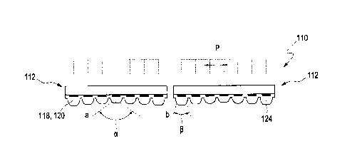
In contrast thereto, Figures 3A and 3B show an embodiment in a view that is
analogous to Fig-
ures 2A and 26, in which the spacing D between the optoelectronic modules 112
is greater. In
this case, the optoelectronic modules 112 are accordingly mounted side by side
such that the
pitch is not maintained. Accordingly, the resulting radiation intensity is not
homogeneous in an
area between the optoelectronic modules 112.
Furthermore, Figure 3A figuratively shows directional characteristics of
individual lenses 124 in
cooperation with the associated optoelectronic components 118 or light-
emitting diodes 120,
which are designated with a and b. For example, these may be edge rays which
extend along a
line at which an electric field strength and/or an intensity have dropped to
half the maximum
value.
Figures 4A and 4B show the effect of a variation in the directivity of the
lenses 124 in a view that
is analogous to Figures 3A and 3B. Hence, a lens 124 is shown in an interior
region of the lens
array, said lens 124 comprising a directional characteristic a, if necessary
in cooperation with the
associated optoelectronic component 118 or light-emitting diode 120, whereas a
lens 124 posi-
tioned at an edge of the lens system 122 of an optoelectronic module 112
comprises a directional
characteristic b. For example, the directional characteristic a may comprise
an emission angle a
whereas the directional characteristic b comprises an emission angle 13. These
different direc-
tional characteristics a, b can, for example, be achieved by varying the lens
form and/or the lens
height and/or the alignment of the lens 124 with the associated optoelectronic
component 118.
For example, a variation of the lens form of the lenses 124 in a side-by-side-
mounting direction
can generate a radiation intensity that is as homogeneous as possible at a
specific distance,
even if side-by-side mounting is effected in a non-pitch-maintaining manner.
By varying the direc-
tivities, the total directivity 130 according to Figure 4B is therefore
considerably more homogene-
ous in an area between the optoelectronic modules 112 than in the embodiment
according to
Figures 3A and 3B. For example, central lenses 124 of the lens arrays can be
configured in a
rather scattering manner, as shown in Figure 4A, and lenses at an edge of the
lens array can be
CA 02842117 2014-01-16
24
configured in a rather collimating manner, as shown in Figure 4A, due to the
smaller emission
angle 13.
As has been described above, a variation in the directivities of the lenses
124 can be achieved in
a variety of manners which can also be combined. For example, Figure 5 shows
an optoelec-
tronic module in which the lenses 124 are decentered and/or otherwise offset
in a targeted man-
ner in relation to the assigned optoelectronic components 118, for example the
light-emitting di-
odes 120. For example, optical axes 132, 133 can be defined for the
optoelectronic components
118 or the assigned lenses 124. For example, an optical axis 132 can be
defined as a straight
line for each optoelectronic components 118, said straight line centrally
extending through an
active surface 136, for example an emission surface, of the optoelectronic
components 118. For
example, an optical axis 134 of the lens can be understood as an axis of
symmetry of the lens
124 wherein, as a matter of principle, asymmetric configurations are, however,
also possible. As
is shown in Figure 5, the optical axes 132, 134 of the components 118, 124
that are assigned to
each other may be offset to each other in parallel. This parallel offset which
is figuratively desig-
nated with 6 in Figure 5 can be designed in a position-dependent manner, as
shown in Figure 5.
For example, an offset 6 = 0 may occur in a centre of the lens array, whereas
an offset that is as
large as possible may occur in an edge region of the lens array. This results
in an asymmetric
directivity in an edge region of the lens array, said asymmetric directivity
being directed more to
the centre of the lens system in the illustrated exemplary embodiment. As an
alternative or in
addition to a pure parallel offset of the optical axes 132, 134, there may
also be an angular offset.
Furthermore, Figure 5 also shows that a height H of the lenses 124 can,
alternatively or addition-
ally, be varied; this also applies to a form of the lenses 124. By taking one,
more or all of the
measures mentioned, it is, for example, all in all possible to achieve an
additional steeper edge
drop in the total directivity 130 for an individual optoelectronic module 112
or a total optoelec-
tronic device 110.
Figures 6A and 6B are a view that is, for example, analogous to Figures 2A and
2B and shows a
section through an optoelectronic device 110 comprising three optoelectronic
modules 112, for
example each according to the embodiment of Figure 5, and an associated total
directivity 130
(Figure 6B). As has been described above, the lens forms of the lenses 124
can, for example, be
varied in a side-by-side-mounting direction (for example, direction X in
Figure 6B) and/or the
lenses 124 can be decentered relative to the optoelectronic components 118 or
light-emitting
CA 02842117 2014-01-16
diodes 120 subject to their array position, and/or the lens height H can be
varied subject to the
array position. For example, this can result in a homogeneous distribution
with a high radiation
intensity at an adjustable working distance, as can be seen from Figure 6B.
While, in the exemplary embodiment according to Figures 4A and 4B, a
directivity with an open-
ing angle 13 was selected at the lenses 124 in an edge region of the lens
array that was smaller
than in a central area, it is, as a matter of principle, also possible to
alternatively or additionally
implement other embodiments. For example, Figures 7A and 7B show an embodiment
in which,
by taking for example one, more or all of the aforementioned measures, lenses
in an inner area
of a lens array comprise a smaller emission angle 13 than lenses in an edge
region (opening angle
a). All in all, a flatter edge drop can, for example, be used to ensure an
additionally increased
radiation intensity at a predetermined, for example adjustable, working
distance from the opto-
electronic device 110.
CA 02842117 2014-01-16
26
List of reference numbers
110 Optoelectronic device
112 Optoelectronic module
114 Chip-on-board module
116 Substrate
118 Optoelectronic component
120 Light-emitting diode
122 Lens system
124 Lens
126 Edge
128 Total directivity for optoelectronic module
130 Total directivity for optoelectronic device
132 Optical axis of the optoelectronic component
134 Optical axis of the optoelectronic lens
136 Active surface