Note: Descriptions are shown in the official language in which they were submitted.
CA 02842963 2014-01-24
WO 2013/037010 PCT/AU2012/001109
1
Giant dielectric constant material
Technical Field
The present invention relates to dielectric materials and to processes for
making
them.
Priority
The present application claims priority from Australian provisional patent
application number AU2011903822, the entire contents of which are incorporated
herein
by cross-reference.
Background
to Driven by
the need to develop high electrical energy storage devices and
miniaturisation of electronic devices down to the micro and/or nanometer
scale;
increasing attention has been concentrated on the development of high or giant
dielectric
constant materials with good thermal stability and low dielectric loss.
To date, there are few materials systems which have a dielectric constant
above 104.
is Examples
include BaTiO3-like perovskite relaxor ferroelectric materials, such as
BaTio 9(Ni, W)0.103, Ba(Feo,5Ta05)03, (Ba, Sr)TiO3, Ba(Ti, Sn)03; CaCu3Ti4012
(CCTO)
as well as analogous compounds like CdCu3Ti4012, Biv3Cu3Ti4012 and
Lao 5Na05Cu3Ti4012 and Li (and/or K), and Ti (and/or V) co-doped NiO. In the
first
BaTiO3-like perovskite system, the giant dielectric constant (about 103-104)
arises from
20 their
relaxor ferroelectric characteristics with a displacive diffuse transition in
the vicinity
of room temperature. The dielectric constant of materials of this type,
however, is
significantly temperature and frequency dependent with a relatively large
dielectric loss.
The giant dielectric constant of the second CCTO-type family of materials can
reach up to
about 103. These CCTO-type materials have relatively better temperature
stability since
25 the high
dielectric polarisation results from both relaxor ferroelectric and internal
barrier
layer capacitance (IBLC) contributions. The dielectric properties of materials
of this type,
however, are often strongly process-dependent. For example, the measured
dielectric
constant can vary over the range from a few hundred up to 105. The doped NiO
and
La2,Srx-Nia4 (x=1/3 or 1/8) systems are ones where the dielectric constant
arises from
30 IBLC or
so called core-shell model contributions. This, again, however leads to a
relatively high dielectric loss over a relatively broad temperature range.
There is therefore a need for a material which exhibits a giant dielectric
constant but
better temperature stability and significantly less dielectric loss by
comparison with
existing giant dielectric constant materials.
CA 02842963 2014-01-24
WO 2013/037010 PCT/AU2012/001109
2
Object
It is an object of the present invention to substantially overcome or at least
ameliorate one or more of the above disadvantages. It is a further objective
to at least
partially satisfy the above need.
Summary
In a first aspect of the invention there is provided a material having formula
A 3+
(0-5n)/3)-05+0xTil-x02. The material may have a rutile structure. It may have
a single
phase rutile structure. In this formula, A3+ is a trivalent positive ion and
B5+ is a
pentavalent positive ion. x should be between 0 and 1 (not inclusive, i.e.
0<x<1). It may
io be such that the material has a rutile structure. 8 may be between 0 and
0.025 inclusive. n
should be between 0 and 0.8 (not inclusive), and may be about 0.5.
The following aspects may be used in conjunction with the first aspect, either
individually or in any suitable combination.
x may be between about 0 and about 0.2 (provided it is not exactly 0). It may
be
s between about 0.0005 and 0.005. x may be such that the dielectric
constant of the material
is greater than about 10,000, or such that the dielectric constant of the
material is between
about 10,000 and 100,000 or between about 10,000 and 1,000,000. x may be for
example
0.0005. It may be 0.005. It may be such that the material has a single phase
ruffle
structure.
20 The material may have a dielectric constant of greater than about
10,000, or
between about 10,000 and 100,000 or between about 10,000 and 1,000,000.
The material may have a dielectric loss of less than about 0.3 at about 20 C.
The
dielectric loss of less than about 0.3 may apply over a temperature range from
about 20 C
to about 200 C. It may be maintained at less than 0.3 over a frequency range
of about
25 100Hz to about 1MHz or of about IkHz to about 1MHz or lkHz to 100MHz.
The material may have a temperature coefficient of its dielectric constant of
less
than or equal to about 1900 ppm/T. The temperature coefficient may be less
than or
equal to about 1900 ppmrC over a range of about 20 C to about 250 C. The
material may
have a positive temperature coefficient of its dielectric constant over a
range of
30 about -100 C to about +200 C or of about -190 C to about +200 C (i.e.
the coefficient
may be positive throughout this range). It may have a temperature coefficient
of its
dielectric constant of less than about 650 ppmft over the range of about -170
C to about
-20 C.
The colour of the material may be grey or may be dark yellow.
CA 02842963 2014-01-24
WO 2013/037010 PCT/AU2012/001109
3
In a particular example the material has a dielectric constant of at least
about 10,000
and dielectric loss of less than 0.3 at about 20 C over a frequency range of
about 1 00Hz
to about 1 MHz.
In the formula 03-1R(4-50)/3)-8B5+0xTi -x02, A3+ may be Bi3+, In3+, Ga3+,
Sc3+, Col,
s Cr3+ , Fe3+ or a trivalent positive ion of a rare earth element or it may
be a mixture of any
two or more of these. A further alternative for A3+ is A13+. B5+ may be Nbs+,
Ta5+, W5+,
V5+, Mos+, and Sbs+ or it may be a mixture of any two or more of these.
The average structure of the material may be a rutile structure. It may be
crystalline.
The material may represent an acceptor-donor co-substitution onto the Ti4+
sites in TiO2
o rutile. =
In an embodiment the material is (A3+0.5_8 B3+o.5)xTi1-x02, wherein x is less
than 0.2
and greater than 0 and 8 is less than about 0.005, said material having a
rutile structure.
In a particular example, the material is (In0.5..5Nbo.5);ri -x02 (i.e.
(In3+ o.5-
61\1135+0.5)r11-x02), where 0<x<0.15, for example 0.0005 to about 0.005, and 8
is less than
is about 0.005. In other examples, A3+ is A13+ and B5+ is Nbs+, whereby the
material has
formula (A13+0.5-81\1b5+0.5)Ji1-x02 or (A13+0 -
.o838Nb5+0.75)xTit-x02.
The material may be in the form of pellets. In this case each pellet may be a
single
phase pellet.
In a second aspect of the invention there is provided a process for making a
material
20 of formula (A3+04-sny3)-5135+0xTii-,02 comprising:
= mixing A203, B205 and TiO2 to form a mixture,
= compressing the mixture to form pellets, and
= annealing the pellets to form the material of formula (A3+o.5-
05+o.$)Jii.x02.
In the formula (A3+o.5-05 o.$)xerii.,,02, 0<x<1 and x is such that the
material has a rutile
25 structure, 8 is between 0 and 0.025 inclusive, n is between 0 and 0.8
inclusive, A3+ is a
+
trivalent positive ion and B5 is a pentavalent positive ion.
The following aspects may be used in conjunction with the second aspect,
either
individually or in any suitable combination.
x may be between about 0 and about 0.1 (provided it is not exactly 0). It may
be
30 between about 0.0005 and 0.005. x may be such that the dielectric
constant of the material
is greater than about 10,000, or such that the dielectric constant of the
material is between
about 10,000 and 100;000, or between about 10,000 and 1,000,000.
The process may be conducted in the solid state.
CA 02842963 2014-01-24
WO 2013/037010 PCT/AU2012/001109
4
The step of annealing may be conducted in a closed furnace. It may be
conducted at
a temperature of between about 1300 to about 1500 C. It may be conducted for
sufficient
time to produce annealed pellets of formula (A3+((4-5n)/3)-8-B5+0011-x02- It
may for example
be conducted for at least about 2 hours or at least about 5 hours, or from
about 2 to about
20 hours or from about 5 to 20 hours.
The molar ratio of A203, B205 and TiO2 may be such that the process produces
the
material of formula (A3+((4-5n)/3)-8/35+10xTi 1-x02. The molar ratio of 4203
to B205 may be
about 1:1 or, more generally, (4-5n):3n. The molar ratio of A203 plus B205 to
TiO2 may
be about (x/2):(1-x) or ((2-3n)x/3): (1-x).
io In a particular example, A is In, B is Nb, n is 0.5 and the step of
annealing is
conducted at about 1450 C for about 10 hours, whereby the process makes
(In 3+-1\11)5+
058 0.5)xTi 1-x02, where 0<x<0.1.
The invention also encompasses a material made by the second aspect. The
material
made by the second aspect may be according to the first aspect.
In a third aspect of the invention there is provided a capacitor comprising a
material
according to the first aspect, or made by the process of the second aspect,
when used as a
dielectric material.
In a fourth aspect of the invention there is provided use of a material
according to
the first aspect, or a material made by the process of the second aspect, as a
dielectric
material.
In a fifth aspect of the invention there is provided use of a material
according to the
first aspect, or a material made by the process of the second aspect, for the
manufacture of
a capacitor.
In a sixth aspect of the invention there is provided a process for making a
capacitor
comprising locating a material according to the first aspect, or a material
made by the
process of the second aspect, between two electrically conductive terminals.
Brief Description of the Drawings
A preferred embodiment of the present invention will now be described, by way
of
an example only, with reference to the accompanying drawings wherein:
Figure 1 shows X-ray diffraction patterns of doped TiO2 rutile at room
temperature;
Figure 2 shows the dielectric frequency spectra of In + Nb doped TiO2 at room
temperature;
Figure 3 shows the dielectric constant and loss tangent of In + Nb doped TiO2
with
respect to dopant concentration;
CA 02842963 2014-01-24
WO 2013/037010 PCT/AU2012/001109
Figure 4 shows a typical curve that describes the relation between dielectric
constant and
temperature for In + Nb doped TiO2 below room temperature range; and
Figure 5 is a curve of (a) dielectric constant and (b) loss at temperatures
above room
temperature for various materials according to the invention.
5 Figure 6 shows frequency dependent dielectric properties of improved
(In+Nb) doped
Ti02.
Figure 7 shows the temperature-dependent dielectric properties of 10% (In+Nb)
doped
Ti02.
Figure 8 shows frequency dependent dielectric permittivity and loss of
to (A10.5Nb0 5)Ti1.,(02 with x=0.5% annealed at 1500 C for 5 hours.
Figure 9 shows frequency dependent dielectric permittivity and loss of
(Alo 053Nb0 75)xTi 1,02 with x=0.5% was annealed at 1500 C for 4 hours.
Detailed Description
The invention relates to materials of chemical formula (443+((4-5n)/3)-
05+0xeri I -x02,
commonly approximately (A3+o5-8115+o.$)Jii_x02. The materials of the invention
have a
rutile structure, commonly a single phase rutile structure. In this formula,
the Ti is at least
partly in the +4 oxidation state (commonly almost entirely in the +4 oxidation
state), and
may also be partially in the +3 oxidation state. The materials may be regarded
as "doped"
titanium dioxides, in which the dopants are A203 and B205, commonly (although
not =
necessarily) in approximately equimolar amounts. Definitions of the variables
in this
formula are' set out below.
A: this is an element capable of forming a +3 ion. Suitable examples
include Sc,
Y, lanthanides (also known as rare earths ¨ La, Ce, Pr, Nd, Pm, Sm, Eu, Gd,
Tb, Dy, Ho,
Er, Tm, Yb, Lu), Al, Bi, Ga, In, Cr, Co and Fe. Mixtures of any two or more,
in any
desired ratio, may also be used. For example the material may for example have
formula
(Aa3 y-6,4b3+05-y-eB5+05);ril-x02, in which 0<y<(0.5-e) (i.e. y is between 0
and 0.5-s
inclusive) and x is such that the material has a rutile structure (in many
cases 0<x<0.15,
or 0<x<0.1, commonly 0.0005<x<0.005) and Aa and A6 are different examples of A
from
the list above. In this case 8+c is between about 0 and 0.025 inclusive and
both 8 and e are
positive numbers or 0. It will be understood that in the more general case
where there are
n moles of B5+ per mole of the material (rather than specifically 0.5 moles),
the above
formula will be adjusted accordingly. In that case, y should be between 0 and
(4-5n)13.
A3+. may be an electron acceptor. A may be a stronger electron acceptor than
Ti.
CA 02842963 2014-01-24
WO 2013/037010 PCT/AU2012/001109
6
B: this
is an element capable of forming a +5 ion. Suitable examples include Nb,
Ta, W, V, Mo, and Sb. Mixtures of any two or more of these may also be used.
For
example the material may have formula (Aa3+y-6/43+o.5-y-efic5+0.5-
zBd5+z)xTii_,,02, in which
00.5 (i.e. both y and z are between 0 and 0.5 inclusive), x is such that the
material has a rutile structure (in many cases 0<x<0.15, or 0<x<0.1, or
0.0005<x<0.005),
ft, and Ab are different examples of A from the list of options for A above
and Be and Bd
are different examples of B from the list of options for B above. In this case
again, 8+c is
between about 0 and 0.025 inclusive. Again, as discussed above, the above
formula may
be generalised for cases in which n is not 0.5 B5+ may be an electron donor. B
may be a
io stronger electron donor than Ti.
In the above formulae, if present, y and z may, independently, be anywhere
between
0 and 0.5, or about 0 to 0.3, 0 to 0.1, 0.1 to 0.5, 0.2 to 0.5, 0.1 to 0.4 or
0.2 to 0.3, e.g.
about 0, 0.05, 0.1, 0.15, 0.2, 0.25, 0.3, 0.35, 0.4, 0.45 or 0.5, with the
proviso that neither
y nor z may be such that the coefficient in which they appear is less than 0.
+
Preferably A and B are such that the material is stable. They may be such that
A3
does not reduce B5+ during formation of the material or in the material
itself.
x: this
should be such that the material has a rutile structure. Also, it should be
such that 0<x<1, so that the material is not pure titanium dioxide but does
contain
titanium. Thus x is such that the material may be seen as a titanium dioxide
of rutile
structure, doped with A and B. It may be equal to or less than about 0.2 or
equal to or less
than about 0.15 or equal to or less than about 0.1. It may be less than or
equal to 0.05,
0.02, 0.01, 0.005, 0.002, 0.001, 0.0005 or 0.0002, provided that it is greater
than 0 (so that
A3+ and B5+ are both present in the material). x may be about 0.0001 to about
0.1 or about
0.0001 to 0.001, 0.0001 to 0.0005, 0.0005 to 0.005, 0.0005 to 0.05, 0.005 to
0.05 or 0.001
to 0.01 e.g. about 0.0001, 0.0002, 0.0003, 0.0004, 0.0005, 0.0006, 0.0007,
0.0008,
0.0009, 0.001, 0.002, 0.003, 0.004, 0.005, 0.006, 0.007, 0.008, 0.009, 0.01,
0.015, 0.02,
0.025, 0.03, 0.035, 0.04, 0.045, 0.05, 0.055, 0.06, 0.065, 0.07, 0.075, 0.08,
0.085, 0.09,
0.095 or 0.1. The limits to the value of x will depend on the nature of A and
B. For a
particular value of x, it may be readily determined, for example by x-ray
diffraction,
whether the resulting ceramic has the required single phase rutile structure
and hence
whether that value of x is appropriate for the particular choice of A and B.
The value of x
may also depend on the value of n (see below) i.e. on the ratio of A and B in
the material.
8: this
is less than 0.025 and may on occasions be effectively 0. The inventors
have found that, whereas nominally the titanium is in the +4 oxidation state,
very small
CA 02842963 2014-01-24
WO 2013/037010 PCT/AU2012/001109
7
amounts (typically less than about 1%) may be reduced to the +3 oxidation
state. In order
to compensate for this, small amounts of the A3+ ion may be lost or oxygen
vacancy may
need to be created. The factor ö reflects this loss. Thus 8 is generally less
than about 5%
of the amount of A3+, i.e. less than about 0.025 (which is 5% of 0.5). It may
be less than
about 0.02, 0.015, 0.01, 0.005, 0.004, 0.003, 0.002, 0.001 or 0.0005. Typical
values of 8
are for example 0.0001, 0.0002, 0.0003, 0.0004, 0.0005, 0.0006, 0.0007,
0.0008, 0.0009,
0.001, 0.002, 0.003, 0.004, 0.005, 0.1, 0.015, 0.02 or 0.025. 8 may be
effectively zero, in
which case effectively all of the Ti is in the +4 oxidation state.
n: this
is commonly around 0.5, however in cases in which n is not 0.5, the
o
material has unequal molar amounts of A3+ and B5+. n may be between about 0
and about
0.8 (but in no case 0 or less, or 0.8 or more), or between about 0 and 0.5 or
0.5 and 0.8 or
0.4 and 0.6 or 0.55 and 0.65 or 0.4 and 0.5 or 0.5 and 0.6, e.g. about 0,
0.05, 0.1, 0.15,
0.2, 0.25, 0.3, 0.35, 0.4, 0.45, 0.5, 0.55, 0.6, 0.65, 0.7, 0.75 or 0.8. The
range for n must
also be adjusted to ensure that the coefficients for the different ions are
greater than 0.
In the formulae above, e.g. in the formula (A3+((4-503)-6135+0xTii_x02, it
should be
recognised that the subscripts represent ratios of numbers of atoms or ions
present in the
material and do not suggest that fractional atoms or ions are actually
present. It should
also be recognised that the formula represents an empirical formula for a
substance which
may not be homogeneous. There may for example be localised regions with
different
zo ratios of atoms/ions. In particular, there may be different
concentrations of particular
atoms/ions in grains comPared to at grain boundaries. The inventors have found
that A3+
ions can in some cases be in higher than average concentration at and/or near
grain
boundaries.
The material may have a dielectric constant of greater than about 10,000, or
greater
than about 11,000, 12,000, 13,000, 14,000, 15,000, 16,000, 17,000, 18,000,
19,000 or
20,000, or of about 10,000 to about 30,000, or about 10,000 to 20,000, 10,000,
to 15,000,
10,000 to 12,000, 10,000 to 11,000, 11,000 to 30,000, 15,000 to 30,000, 20,000
to 30,000,
11,000 to 15000, 11,000 to 13000 or 15,000 to 20,000, e.g. about 10,000,
10,500, 11,000,
11,500, 12,000, 12,500, 13,000, '13,500, 14,000, 14,500, 15,000, 16,000,
17,000, 18,000,
19,000, 20,000, 21,000, 22,000, 23,000, 24,000, 25,000, 26,000, 27,000,
28,000, 29,000
or 30,000. In some cases the dielectric constant may be above 30,000, e.g.
about 35,000,
40,000, 45,000, 50,000, 60,000, 70,000, 80,000, 90,000 or 100,000. Particular
examples
of these materials have dielectric constants above 100,000, and may have a
dielectric
constant over 200,000, 300,000, 400,000, 500,000, 600,000, 700,000, 800,000,
900,000
CA 02842963 2014-01-24
WO 2013/037010 PCT/AU2012/001109
8
or 1,000,000. Thus the dielectric constant may be between about 10,000 and
about.
1,000,000, or 100,000 to 1,000,000 or 100,000 to 500,000 or 500,000 to
1,000,000, e.g.
about 200,000, 300,000, 400,000, 500,000, 600,000, 700,000, 800,000, 900,000
or
1,000,000.
The material may have a dielectric loss of less than about 0.3 at about 20 C
or less
than about 0.25, 0.2, 0.15 or 0.1, e.g. about 0.05 to 0.3, 0.1 to 0.3, 0.2 to
0.3, 0.1 to 0.25 or
0.15 to 0.25. It may have a dielectric loss at about 20 C of about 0.1, 0.15,
0.2, 0.25, 0.25,
0.27, 0.28, 0.29 or 0.3. The dielectric loss may be less than about 0.05 at
about 20 C or at
about 27 C, or less than about 0.045, 0.04, 0.035, 0.3, 0.025 or 0.02, or may
be about 0.1,
0.2 or 0.3 at these temperatures. The dielectric loss (or range thereof) as
described above
may apply over a temperature range from about 20 C to about 200 C, or about 20
to 150,
to 100, 20 to 50, 50 to 200, 100 to 200, 150 to 200 or 50 to 150 C. It may for
example
apply at any one or more of the following temperatures: 20, 25, 30, 35, 40,
45, 50, 55, 60,
65, 70, 75, 80, 85, 90, 95, 100, 110, 120, 130, 140, 150, 160, 170, 180, 190
or 200 C. It
15 may also
apply at other temperatures outside the above ranges, e.g. at about 0, 5, 10,
15,
210, 220, 230, 240 or 250 C. It may apply from about -190 to about 250 C, or
about -100
to 250,,0 to 250, 100 to 250, -190 to 100, -190 to 0, -190 to -100, -100 to
200, -100 to 0 or
-50 to 150 C, e.g. about -190, -150, -100, -50, 0, 20, 50, 100, 150, 200 or
250 C. Suitable
materials have dielectric loss of less than about 0.1, commonly less than
about 0.05,
20 across a
temperature range of about -190 to about 200 C or about -190 to about 250 C.
The dielectric loss as described above may be maintained over a frequency
range of about
100Hz to about 1MHz, or about 1 kHz to about 1MHz, or about 1 to 500kHz, 1 to
200, 1
to 100, 1 to 50, 1 to 20, 1 to 10, 10 to 200, 10 to 100, 10 to 50, 50 to 1000,
100 to 1000,
200 to 1000, 500 to 1000, 100 to 500, 100 to 300 or 200. to 500kHz, e.g. about
1, 2, 3, 4,
5, 6, 7, 8, 9, 10, 20, 30, 40, 50, 100, 150, 200, 150, 300, 350, 400, 450,
500, 600, 700,
800, 900 or 1000kHz. It may also be maintained beyond these ranges. In some
instances
the dielectric loss is maintained as described above up to about 100MHz. It
may therefore
be maintained in the range of about lkHz to about 100MHz, e.g. from about 1 to
about
100MHz, or about 1 to 50, 1 to 10, 10 to 100, 50 to 100 or 10 to 50MHz, e.g.
about 1, 2,
3, 4, 5, 10, 15, 20, 25, 30, 35, 40, 45, 50, 60, 70, 80, 90 or 100MHz.
Suitable materials
therefore may maintain a dielectric loss of less than about 0.1, commonly less
than about
0.05, over a range of about 100Hz to about 1MHz, or lkHz to about 100MHz. From
the
above, it should be understood that any combination of dielectric loss,
temperature range
and frequency range, each within the ranges above, may apply. Where it is
stated that the
CA 02842963 2014-01-24
WO 2013/037010 PCT/AU2012/001109
9
dielectric loss of less than about 0.3 applies over a particular temperature
and/or
frequency range, this does not necessarily indicate that a particular value of
the loss
applies over the whole range, but rather that over the whole range the loss is
less than 0.3,
even though there may be some variation within the range.
The material of the invention has a relatively constant dielectric constant
over a
range of temperatures. Thus over a selected temperature range it may have a
temperature
coefficient of its dielectric constant of less than or equal to about 2000
ppm/T, or less
than or equal to about 1900, 1500, 1200, 1000, 500, 200 or 100 ppm/T. This
coefficient
(or range thereof) may be maintained over a range of about 20 C to about 250
C, or about
io 20 to 200, 20 to 150, 20 to 100, 50 to 250, 100 to 250, 150 to 250,
100 to 200, 100 to 150
or 150 to 200 C. In particular it may apply at any one or more of the
following
temperatures: 20, 25, 30, 35, 40, 45, 50, 55, 60, 65, 70, 75, 80, 85, 90, 95,
100, 110, 120,
130, 140, 150, 160, 170, 180, 190 or 200 C. It may also apply at temperatures
outside that
range, e.g. at about 0, 5, 10, 15, 260, 270, 280, 290 or 300 C. It may apply
from.about -
s 190 to about 250 C, or about -100 to 250, 0 to 250, 100 to 250, -190
to 100, -190 to 0, -
190 to -100, -100 to 200, -100 to 0 or -50 to 150 C, e.g. about -190, -150, -
100, -50,0, 20,
50, 100, 150, or 200 C. The temperature range may be frequency dependent. Thus
at low
frequencies (e.g. around 100Hz or less), the upper temperature limit may be
lower, e.g.
about 200 C whereas at higher frequencies (i.e. greater than about 100Hz) a
higher upper
20 temperature limit may be attainable, e.g. about 250 C. Higher
frequencies may be useful
in enabling the material to be used in radio frequency communication
technology.
Suitable materials have dielectric loss of less than about 0.1, commonly less
than about
0.05, across a temperature range of -190 to about 200 C. The material may have
a
positive (or non-negative) temperature coefficient of its dielectric constant
over a range of
25 about -100 C to about +200 C, or about -100 to +100, -100 to 0, 0 to
+200, +100 to +200
or 0 to +100 C, e.g. it may have a positive (or non-negative) temperature
coefficient of its
dielectric constant at or about any one or more of the following temperatures:
-100, -50,
0, +50, +100, +150 or +200 C. It may have a positive (or non-negative)
temperature
coefficient at temperatures outside the above ranges. It may have a
temperature
30 coefficient of its dielectric constant of less than about 650 ppmiT,
or less than about 600,
550, 500, 540, 400, 350, 300, 250, 200, 150 or 100 pp/1/ C (e.g. the
coefficient may be
about 600, 550, 500, 540, 400, 350, 300, 250, 200, 150 or 100 ppiniT). This
may apply
over the range of about -170 C to about -20 C, or about -150 to -20, -100 to -
20, -50 to -
20, -170 to -50, -170 to -100, -100 to -50 or -150 to -100 C, e.g. atabout, -
170, -160,
CA 02842963 2014-01-24
WO 2013/037010 PCT/AU2012/001109
150, -140, -130, -120, -110, -100, -90, -80, -70, -60, -50, -40, -30 or -20 C.
It may also
apply outside these ranges, e.g. at about 0, -5, -10, -15, -175, -180, -185, -
190, -195 or -
200 C.
The average structure of the material may be a rutile structure. The material
may
5 represent
an acceptor-donor co-substitution onto the Ti4+ sites in TiO2 rutile. The
average
structure may have a space group P42/mnm. The material may be in the form of
pellets.
The term "pellet" may be taken to include all manner of pellet-like structures
such as
granules or grains or particles. In this case each pellet or granule or grain
or particle may
be a single phase pellet or granule or grain or particle. These may be
spherical, or may be
io some
other suitable shape, for example ovoid, ellipsoid, cubic, rhomboidal,
prismatic,
parallelepiped (for example rectangular parallelepiped), oblate spherical,
acicular, fibrous,
toroidal, polyhedral (with between about 6 and about 50 sides), platelet-
shaped,
rhomboidal or may be irregular shaped. Different pellets may have the same
shape or may
have different shapes. The pellets may have a diameter of about 5 to about 15
mm, or
about 5 to 10, 10 to 15 or 8 to 12 mm, e.g. about 5, 6, 7, 8, 9, 10, 11, 12,
13, 14 or 15 mm.
They may have a thickness of about 0.1 to 2mm, or about 0.1 to 1, 0.1 to 0.5,
0.5 to 1 or 1
to 2mm, e.g. about 0.1, 0.2, 0.3, 0.4, 0.5, 0.6, 0.7, 0.8, 0.9, 1, 1.5 or 2mm.
They may for
example have a diameter of about 10 to about 12mm and a diameter of about lmm.
Commonly the doping concentration is from about 0.05-10 mol%, commonly about
zo 0.05-5
mol%, because higher doping concentrations frequently result in higher loss.
As
noted earlier, however, this limit may depend on the ratio and nature of A and
B. A
suitable balance between dielectric constant, loss and temperature stability
is required for
practical applications. At this level of doping, it has been observed that the
material
retains a rutile structure, which is considered important for keeping
dielectric loss low.
Tetravalent doping ions have not been found to be effective in the present
invention
because they only change the polarisability and are not capable of providing
sufficient
driving force to increase the dielectric constant up to the desired minimum of
about 104.
Trivalent ion doping is capable of maintaining the dielectric constant as
similar to that of
pure Ti02. Pentavalent ion doping is capable of significantly changing the
material
properties from insulating to semi-conducting and -consequently can lead to
very high
loss. The inventors hypothesise that the underlying mechanism relates to:
(1) the donor-acceptor pairs can attain overall charge balance, however the
= pentavalent ions have a potential to locally induce the Ti ion valency
change from Ti4+
CA 02842963 2014-01-24
WO 2013/037010 PCT/AU2012/001109
11
into Ti3f. Ti3+ has an unpaired electron which is localised to form dipoles
and contribute
to the observed dielectric constant; and
(2) the doping ions create semi-conductive barrier layers in the grain
boundary to
form the internal barrier layer capacitors (IBLCs) and hence lead to the high
dielectric
constant.
The process for making the materials of the invention may be a solid state
process.
It may be a solvent free process. It may be conducted in the absence of
solvents. It may be
conducted without addition of substances other than the component oxides (see
below). In
order to make the materials of the invention, a mixture of component oxides
A203, B205
and TiO2 (where A and B are as defined above) is compressed compressing the
mixture to
form pellets. Thus the mixture may comprise, or may consist essentially of,
A203, B205
and Ti02. The mixing of the oxide components should be in suitable proportions
that the
final mixture has a molar ratio of A:B = ((4-5n)/3):n, commonly 1:1. The
proportions
should be such that the ratio of (A+B):Ti is about x:(1-x). Thus the molar
ratio of A203 to
is B205 should be about ((4-5n)/3):n, commonly about 1:1. In the case where
n is about 0.5,
the molar ratio of A203 to B205 may be between about 0.9:1 and 1.1 to 1, or
about 0.9:1
and 1:1, 1:1 and 1.1:1,0.95:1 and 1.05:1, 0.95:1. and 1:1, 1:1 and
1.05:1,0.99:1 and
1.01:1, 0.99:1 and 1:1, 1:1 and 1.01:1, 0.999:1 .and 1.001:1, 0.999:1 and 1:1
or 1.001:1
and 1:1, e.g. about 0.9:1, 0.91:1, 0.92:1, 0.93:1, 0.94:1, 0.95:1, 0.96:1,
0.971, 0.98:1,
20 0.99:1, 0.995:1, 0.999:1, 1:1, 1.09:1, 1.08:1, 1.07:1, 1.06:1, 1.05:1,
1.04:1, 1.03:1, 1.02:1,
1.01:1, 1.005:1 or 1.001:1. For other values of n, the molar ratio will of
course be
correspondingly different. The actual weight ratio will depend on the atomic
weights of A
and B. The molar ratio of A203 and B205 combined to TiO2 should be (x/2):(1-
x). In many
(but not all) instances, x is less than about 0.2. Consequently the molar
ratio of A203 and
25 B205 combined to TiO2 will generally be 1:t, where t is greater than
about 8. t may be for
example greater than about 8, 9, 10, 12, 14, 16, 18, 20, 25, 30, 35, 40, 45,
50, 100, 200,
300, 400, 500 or 1000, or may be about 8 to about 1000 or about 8 to 1000, 8
to 500, 8 to
200, 8 to 100, 8 to 50, 8 to 20, 10 to 1000, 15 to 1000, 20 to 1000, 50 to
1000, 100 to
1000, 200 to 1000, 500 to 1000, 20 to 100, 50 to 100, 20 to 50 or 50 to 200,
e.g. about 8,
30 9, 10, 11, 12, 13, 14, 15, 16, 17, 18, 19, 20, 21, 22, 23, 24, 25, 30,
35, 40, 45, 50, 60, 70,
80, 90, 100, 150, 200, 250, 300, 350, 400, 450, 500, 600, 700, 800, 900 or
1000. Again,
the weight ratio will depend on the atomic weights of A and B. The component
oxides
(A203, B205 and Ti02) may have similar grain sizes when forming the mixture.
They may
CA 02842963 2014-01-24
WO 2013/037010 PCT/AU2012/001109
=
12
have grain sizes that do not vary from each other by more than about 30%. The
mean
grain size (i.e. grain diameter) may be of the order of microns.
The mixing of the component oxides to form the mixture may comprise combining
and subsequent and/or simultaneous agitation (swirling, stirring, shaking,
tumbling etc.).
The agitation may be sufficient to generate a substantially homogeneous
mixture. In this
context, a homogeneous mixture is one in which the mole ratios of the elements
A, B and
Ti are substantially even through the mixture, i.e. the components are
substantially evenly
distributed through the mixture. The components may be mixed in any order, or
all
together, provided that the final mixture has the required composition as
described above.
io The step of compressing may be conducted using a press (e.g. a hydraulic
press), a mould,
a pelletiser or some other suitable compression device. The compressing may be
at a
sufficient pressure to convert the mixture into pellets. It may be uniaxial
compressing. It
may be at a pressure of about 3 to about 15 tonnes, or about 3 to 10, 3 to 5,
5 to 15, 10 to
or 5 to 10 tonnes, e.g. about 3, 4, 5, 6, 7, 8, 9, 10, 11, 12, 13, 14 or 15
tonnes. It may be
s . conducted at about room temperature, or at about 15 to about 300, or
about 15 to 20, 20 to
30 or 20 to 25 , e.g. about 15, 20, 25 or 30 .
The resulting pellets are then annealed in order to produce the final
material. The
step of annealing may be conducted in a closed furnace. A suitable furnace has
chamber
dimensions of about 15mm x 15mm x 15mm. It may be conducted at a temperature
of
between about 1300 to about 1550 C, or about 1300 to 1500, 1300 to 1400, 1400
to 1500
or 1350 to 1450 C, e.g. at about 1300, 1310, 1320, 1330, 1340, 1350, 1360,
1370, 1380,
1390, 1400, 1410, 1420, 1430, 1440, 1450, 1460, 1470, 1480, 1490, 1500 or 1550
C. It
may be conducted for sufficient time to produce annealed pellets of formula
(A3+((4-503)-
isx02. This may be accompanied with a minor loss of A3+ ions, accounted for by
the factor 8 in the formula. It may for example be conducted for at least
about 5 hours, or
at least about 6, 7, 8, 9, 10 or 15 hours, or from about 5 to about 20 hours,
or about 5 to
10, 10 to 20 or 10 to 15 hours, e.g. about 5, 6, 7, 8, 9, 10, 11, 12, 13, 14,
15, 16, 17, 18, 19
or 20 hours. Any combination of the above temperatures and times may be
suitable in
particular cases. The resulting pellets may for example have a mean diameter
of about
9mm and a thickness of about 0.6 mm.
The inventors have found that, although many suitable materials according to
the
invention have equal quantities of A and B, the ratio of A:B does not have to
be exactly
1:1. A more important restriction is from the overall structure of the
material: it should
retain a single rutile phase. As long as the overall charge is balanced,
therefore, n need not
CA 02842963 2014-01-24
WO 2013/037010 PCT/AU2012/001109
13
be 0.5 (i.e. A:B need not be 1:1). In the case of excess B (n>0.5) , it is
considered that
there are Ti4+-Ti3+, B5+-Ti3+ or B5+-Ti3+-A3+ conjunctions coexisting in the
compound. In
the case of less B (n<0.5), Ti4+-A3+, B5+-Ti3+ or B5+-Ti3+-A3+ conjunctions
coexist. In the.
equimolar case (n=0.5), there will be predominantly B5+-A3+-Ti3+ conjunctions.
It is
recognised that TiO2 has quite large capability to accommodate the 3+ cation
via the
shear planes where some cations occupy the interstices.
The inventors hypothesise an electron-pinned defect-dipole mechanism to
explain
the large dielectric constants of the materials described herein. In this
mechanism,
hopping electrons are captured and localized by designated lattice defect
states ("pinning
o effect") to generate gigantic defect-dipoles and result in high-
performance extremely
large permittivity materials. The inventors therefore consider that they have
created
electron-pinned defect-dipoles in titanium oxides in a way that electrons are
pinned
surrounding the titanium oxygen polyhedra (Ti00,0) with less freedom. As these
electrons have more space (within a several polyhedra region) for motion in
comparison
is to the electrons in atoms, the resultant dipoles are gigantic and the
behaviors of these
dipoles still behave like "intrinsic" lattice defect dipoles rather than free
electron
hopping. In order to achieve this the inventors introduced a donor
substitution to ensure
that the host is dominated by delocalized electrons originating from the
reduction of the
host atom nearby. The newly created oxygen vacancies or oxygen deficient
enviornrnent
20 (positive charge centres) are created by incorporating another acceptor
heteroatom into
the host lattice and then combining with originally delocalized electrons to
form defect
dipoles. Most importantly, the whole of designated material system is charge
balanced,
giving less flexibility to localization of the doping induced behaviours. As
the most
important consequence of the formation of such local defect-dipoles, apart
from the very
25 large permittivity, extremely low dielectric loss is obtained. It is
hypothesised that this is
because the electron is bonded by the locally created oxygen deficient
environment to
form a gigantic dipole which can respond to an external electrical field,
rather than an
electron hopping from one lattice site to another.
The material of the invention may be used as a high dielectric material in
30 capacitors. Due to the very high dielectric constant, described earlier,
the material is
suitable for use in producing capacitors with very high capacitance, or else
for use in
producing very small capacitors. It also has a strong potential to be used in
safe, high
efficiency solid state energy storage devices, such as a super- and/or ultra-
capacitor
material.
CA 02842963 2014-01-24
WO 2013/037010 PCT/AU2012/001109
14
The present invention therefore relates to new giant dielectric constant
materials.
Certain of these materials may be useful in the miniaturisation of electronic
devices
=
and/or in the fabrication of high electrical energy storage devices. They may
have a
dielectric constant of over 10,000 with a relatively low dielectric loss and
moderately
good temperature stability over a very broad temperature range. These
properties are
superior by comparison with existing materials systems performing a similar
function
The present invention is of significance as materials described herein display
a giant
dielectric constant over an broad temperature range, not uncommonly from
liquid
nitrogen temperature (about 77K) up to about 200 C with the dielectric loss
over this
o entire temperature range being less than about 0.3.
The invention relates generally to modified rutile type electroceramics, e.g.
(In,Nb,Ti)02, and their use as a giant dielectric constant material. The
inventors disclose
herein a design strategy for producing significantly less lossy, giant
dielectric constant
materials with a feasible temperature stability for practical applications.
The process for
making the materials of the invention appears to represent a donor-acceptor co-
substitution into TiO2 rutile. It is thought that the crystal chemical co-
substitution
principle avoids the appearance of intrinsic defects like oxygen vacancies,
cation
vacancies and Ti3+ interstitial ions. This design principle also provides the
ability to
control the formation and concentration of Ti3+ ions and to accommodate (or
release)
zo local strains created by the Ti3+ cations and associated structural
distortion, which will
consequently localise the quasi-free electron from the Ti3+ cations, enhance
dielectric
polarisation, reduce the dielectric loss and improve temperature stability.
The materials of the invention have a general chemical formula of
(A3+,B5+),,Tii-x02
where A3+ is a trivalent transition metal ion such as Bi3+, In3+, Ga3+ or the
3+ ion of a rare
earth element, or may be a mixture thereof, and B5+ is a pentavalent ion such
as Nb5+, W5+
or Ta5+ ions or a mixture thereof. These compounds commonly have a giant
dielectric
constant, e.g. over 10,000, reasonable dielectric loss and good temperature
stability. The
process described herein for making these materials includes synthesis
procedures and
processing conditions required to obtain a high dielectric constant material
over 10,000
with a dielectric loss less than 0.3 and a relatively good temperature
stability over a broad
temperature range, for instance less than 1900 ppm/K over the temperature
range from
. room temperature up to 200 C. Thus the present specification describes
the following:
= Design strategy: acceptor-donor co-substitution onto the Ti4+ sites in
TiO2 rutiles
according to the chemical formula (A3+,B5+),,Ti1_x02). In many, but not all,
cases the mole
CA 02842963 2014-01-24
WO 2013/037010 PCT/AU2012/001109
ratio of A to B is equal to 1, that is, the material has formula (A3+0 sz-B5+0
sVrii_x02, and x
is such that the material has a rutile structure (e.g. 0<x<0.1 or
0.0005<x<0.005) and 8 is
between 0 and 0.025 inclusive.
= Trivalent ions including, but not limited to, Al3+, Bi3+, In3+, Ga3+ and
rare earth
s elements as well as mixtures thereof are candidates for acceptor ions
(A3+) to be doped
into TiO2 rutile.
= Pentavalent ions including, but not limited to, Nb5+, Ta5+, W5+ as well
as mixtures
thereof are candidates as donor ions (B5+) to be doped into TiO2.
= Pentavalent donor ions including Nb5+, Ta5+, W5+ as well as mixtures
thereof may
io induce the reduction of neighbouring Ti4+ ions into Ti3+ ions in TiO2 in
the absence of
neighbouring trivalent acceptor ions A3+. The maximum amount of Ti3+ ions is
therefore
controlled by the concentration of dopant pentavalent ions B5+.
= An approach to synthesise 03+((4-5)/3)-05+=)xTii-,02rutiles, where A =
Bi, In, Ga, Al
or a rare earth element or mixtures of any two or more of these, B = Nb, W and
Ta or
Is mixtures of any two or more of these, including (In0.5.aNbo 5)011,02 by
solid state
reaction.
= A procedure to synthesize dense and well-crystallised (A34((4-5n)/3)-
8135+0xTil-x02
electroceramic pellets by mixing together A203, B205 and TiO2 raw oxide
powders,
pressing the resultant powder into pellets, followed by annealing in a closed
furnace over
the temperature range from 1350T-14507C.
= A procedure to synthesize In3+ and Nb5+ co-doped TiO2 rutile
electroceramics by
mixing In203, Nb205 and TiO2 oxide powders according to the chemical
composition
(In05.,5Nb0.5)Til,02 required, pressing the resultant powder into pellets,
followed by
annealing in a closed box furnace at a temperature in the vicinity of 1450 C
for 10 hours
to produce dense and well-crystallised ceramic pellets.
= An electroceramic as described above, in which the average structure of
the
resultant material is of the rutile structure type.
= An electroceramic as described above in the form of pellets which are
single phase.
= (A3+ (0-503)-8135+ OxIii-x02electroceramic pellets having high dielectric
constants of
over 20000 (up to 40000) and dielectric loss of less than 0.3 at ambient
temperature over
a broad frequency range from 1 kHz to 1MHz.
= (A3+((4_50/3)..8B5+,,),,Tii,02 electroceramic pellets having high
dielectric constants of
over 10000 and dielectric losses of less than 0.3 at ambient temperature over
a broad
frequency range from 1 kHz to 1MHz.
CA 02842963 2014-01-24
WO 2013/037010 PCT/AU2012/001109
16
= 03+((4-5n)/3)-8B5+0xTi 1-x02 electroceramic pellets having high
dielectric constants of
over 20000 and dielectric losses of less than 0.15 at ambient temperature at
1MHz.
= (A34-(0-503)-05+n)Jii,02 compounds have a positive temperature
coefficient of
dielectric constant from -100 C to +200 C.
= The (A3+(0-5ny3)-sen/xTit.x02 compounds have a temperature coefficient of
dielectric constant of 620 ppini1C from -170 C to -20 C, or of no more than
620 ppmJ C
from -170 C to -20 C.
= The (A3+(0-503)-8-135+0xTii-,02 compounds have a temperature coefficient
of
dielectric constant of 1900 ppm/ C from room temperature up to 250 C.
= The electroceramic materials have a dielectric loss less than 0.3 in the
temperature
range from room temperature up to 200 C.
= The method can be widely used to manufacture all the acceptor-donor co-
doped
TiO2 rutile materials.
The materials of the invention may be used to make small capacitance
components.
s For
instance a single layer capacitor with a diameter of 4.7 mm and a thickness of
0.4 mm
can have a capacitance of about 52 nF. This capacitance is over 200 times
higher than the
same sized pure TiO2 capacitor. Conversely, for the same capacitance, the size
of the
capacitor (ratio of area to thickness) may be reduced to 0.5% of the
corresponding pure
TiO2 capacitor.
The temperature stability of these prototype capacitors mostly satisfy the
requirement of standard X7R capacitor codes, which presents a significant
potential for
practical applications. The exact composition of the material with a giant
dielectric
constant may be optimized according to specific requirements of users (such as
temperature stabilisation over a different temperature range or a different
dielectric loss
requirement).
Figure 1 shows X-ray diffraction patterns of doped TiO2 rutile at room
temperature.
The XRD patterns show that the doping does not alter the average rutile
structure of TiO2
for in+Nb doping concentrations in the range of 0.05% to 5%. With increasing
dopant
concentration, the patterns slightly shift towards lower angle. As this
decrease in angle
generally indicates an increase in unit cell parameters, this may provide
evidence that In3+
and Nb5+ ions substitute for TO+ within the lattice, as the average radius of
In3++ Nb5+ is
larger than Ti4+.
Figure 2 shows the dielectric frequency spectra of In + Nb doped TiO2 at room
temperature. From this figure, it can be seen that the dielectric polarisation
in the lower
CA 02842963 2014-01-24
WO 2013/037010 PCT/AU2012/001109
17
frequency range arises from space charges that can contribute to electronic or
ionic
conductive behaviour. As a result, the dielectric constant is higher but
slightly decreases
while the loss decreases significantly with the increasing the frequency.
Debye-type
dielectric polarisation relaxation is also observed in the frequency range
over 1 KHz,
where the dielectric constant has a decreasing step but there are dielectric
loss peaks in
corresponding frequency range. Both dielectric constant and loss show less
dependence
on the frequency in higher frequency range close to 1 MHz, suggesting that
this type of
material may be suitable for use in high frequency energy storage.
Figure 3 shows the dielectric constant and loss tangent of In+Nb doped TiO2
with
io respect
to dopant concentration. It is found that the dielectric constant of doped
TiO2 is
over 2x10⁴, and the corresponding loss is lower than 0.15 measured at 500 KHz.
Figure 4 shows a typical curve that describes the relation between dielectric
constant and temperature below the room temperature range. It is clear that
doped TiO2
keeps its high dielectric substantially constant across the measured
temperature range. Its
temperature coefficient of dielectric constant is less than about 650 ppm/ C
over the range
of about -170 C to about -20 C.
Figure 5 shows the dielectric constant (a) and loss (b) of In+Nb doped TiO2 at
temperatures above room temperature. These curves indicate that the doped TiO2
has
extremely week temperature dependence in the temperature range from room
temperature
to about 200 C, suggesting its excellent temperature stability (the
temperature coefficient
of dielectric constant is approximately less than 0.2%) and high energy
storage ability. In
Fig. 5, the different curves represent data obtained at different frequencies.
The solid
curves were measured at 1 kHz, the dashed curves at 10kHz and the dotted
curves at
100kHz.
Figure 6 shows frequency dependent dielectric properties of (In+Nb) doped TiO2
with different (In+Nb)concentration from 0.05 % to 0.5% to 5% to 10% after
optimisation
of the processing conditions and approaches, such as using ball milling,
adding additives
and varying the annealing temperature and dwelling time, as well as the rising
rate of the
temperature.
Figure 7 shows the temperature-dependent dielectric properties of 10% (In+Nb)
doped TiO2 after optimisation of the processing conditions and approaches,
such as using
ball milling, adding additives and varying the annealing temperature and
dwelling time,
as well as the rising rate of the temperature.
CA 02842963 2014-01-24
WO 2013/037010 PCT/AU2012/001109
18
Thus the inventors have developed a material suitable for use in high
performance
solid state super (ultra) capacitors. There is at present no competing
material and related
super (or ultra) capacitor product currently in the commercial market place,
because all
existing giant dielectric constant materials have problems such as high
dielectric loss,
poor temperature-stability and/or unreproducible processing conditions. Thus
the use of
the present invention for the development of super (ultra) capacitors has
significant
commercial potential. Advantages of the present invention include:
= Simple host compound and simple processing: TiO2 rutile is a simple
compound.
For example it only needs 0.05% co-doping of 1113+ and Nb5+ (representing
x=0.0005 in
to the formula (A3r+05-sB54.o.5);Fit_x02) to achieve a very high dielectric
constant. One step
only sintering is sufficient to achieve dense and high quality crystallised
samples.
= A unique feature of the present invention is that both the temperature
coefficient of
the dielectric constant as well as the dielectric loss tangent are relatively
low, which is a
major advantage.
is = The materials of the invention may be made without use of toxic
elements or
compounds.
Example 1
A bulk quantity of each raw reagent was extracted from its storage container
and
placed into a 150 C oven for a period >12 hours in order to remove any
residual traces of
zo H2O. High purity (>99.9%) Indium Oxide (In203), Niobium Oxide (Nb205)
and TiO2
powders were then weighed into sterile weighing containers in the amounts
displayed in
Table 1 and vigorously mixed under ethanol, by hand, using an agate mortar and
pestle
for >15 minutes. The mixed powders were left to dry at room temperature, heat
treated at
150 C for about 1 hour and then inserted into a stainless steel cylindrical
die and
25 compacted through the application of about 4.5 metric tonnes pressure to
form a
cylindrical 'disk' shaped sample of diameter 13mm. These were sintered in a
box furnace
at a setting of I400 C for 10 hours to form dense, crystalline ceramic
pellets. The
dielectric constant and dielectric loss curves of these sintered pellets
measured over
temperatures spanning from ambient room temperature (about 23 C) to 400 C are
shown
30 in Figure-5a and Figure 5b respectively. These figures demonstrate that
the samples have
a dielectric constant well in excess of 4x10⁴ and an extremely low loss
tangent (about
0.15) for high permittivity materials, particularly at temperatures less than
200 C.
Table 1: Weighing measurements for Nb and In substituted TiO2
CA 028 42 9 63 20 14 - 0 1-24
WO 2013/037010 PCT/AU2012/001109
19 =
, - Total ,
-
= % qn203 Nb2O5 -TiO2
Sample Description
- & (grams) (grams),
Nb(0.00025)In(0.00025)11(0.9995)02 0.05 0.0003 0.0003 0.7986
Nb(0.0025)In(0.0025)Ti(0.995)02 0.50 0.0035 0.0033 0.7950
Nb(0.005)In(0.005)T 40.99)02 1.00 0.0069 0.0066 0.7910
1\lb(o.ot 5)In(0.015)11 (0.97)02 3.00 0.0208 0.0199 0.7750
Nb(0.025)In(0.025)11(0.95)02 5.00 0.0347 0.0332 0.7591
Example 2
TiO2 (99.99%, crystalizing in rutile was provided by Aldrich Co., Nb205
(99.99%)
s was
provided by Stanford Materials Co. and 1n203 (99.99%) was provided by Aldrich
Co.
These were stored at 200 C to completely remove any adsorbed water. The
ceramics of
(Nb+In) co-doped rutile TiO2 [formula: (In0.5Nb0.5)Ti1_x02 ] were prepared by
conventional solid state methods, similar to the process described in Example
1 apart
from using ball milling to replace hand grinding described in Example 1.Here,
x is the
to doping
level of Nb and In. Synthesis conditions for final ceramics were optimized. to
1400 C for the annealing temperature, 10h for the duration time and 2 C/ mm
for rising
rate. The same synthesis procedure was also used for other samples where the
In was
replaced by either Al, or Ga or Sc. The only difference was that the annealing
temperature
was optimised for different elements.
15 High
permittivity with relatively low dielectric loss was achieved due to the
formation of local electron-pinned defect-dipoles via a simultaneous
incorporation of
donor Niobium (Nb) and acceptor Indium (In) into rutile TiO2 host, i.e.
(In0.5Nb0.5)Ji1,02. An extremely low doping level of (Nb+In) was found to give
rise to
very large permittivity at room temperature, e.g. for 0.05% (Nb+In) dopants,
the
20
permittivity was as high as about 2x10⁴, while the dielectric loss (tan 8) was
below 0.05.
Higher doping levels make the permittivity nearly frequency-independent whilst
keeping
tan 8 still below 0.04, especially about 0.02 for 10% (Nb+In) dopants in a
broad
frequency range, even though the permittivity had already incrementally
increased up to
about 6x10⁴. However, a doping level of beyond 10 %, e.g. 20%, led to the
appearance of
CA 02842963 2014-01-24
WO 2013/037010 PCT/AU2012/001109
interfacial polarization which dominates the relatively high dielectric loss,
and also the
huge increase in low-frequency permittivity due to the appearance of the
second impurity
phase.
Another important consequence of the formation of electron-pinned defect-
dipoles
5 was that the colossal permittivity and dielectric loss (tan 6), showed
nearly temperature
independent across the range of 80K to 450K. No low-temperature dielectric
relaxations
were detected even when the temperature dropped close to liquid nitrogen
temperature.
Example 3
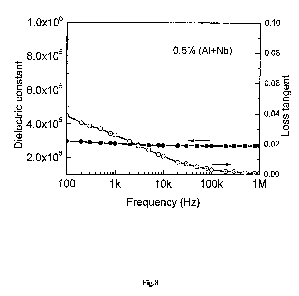
(A10.5Nbo.5)xTi1_x02 with x=0.5% was annealed at 1500 C for 5 hours. Figure 8
shows the
to frequency dependent dielectric permittivity and loss of the resulting
product. A high
dielectric permittivity over 300,000 was achieved with overall loss less than
0.05 in a
broad frequency range at room temperature. .
Example 4
(A1008Nbo.75);Ti1-x02 with x=0.5% was synthesized at 1500 C for 4 hours.
Figure 9
is shows the frequency dependent dielectric permittivity and loss of this
product, giving the
dielectric permittivity over 10,000 and loss less than 0.1.
=
=