Note: Descriptions are shown in the official language in which they were submitted.
CA 02845438 2014-03-12
Attorney Docket No. 1123P002W001
=
CIRCUIT AND METHOD FOR USE IN TRANSCRANIAL MAGNETIC
STIMULATION
TECHNICAL FIELD
[0001] The present invention relates to transcranial magnetic
stimulation (TMS). More specifically, the present
invention relates to systems and circuits for use with
TMS systems.
BACKGROUND OF THE INVENTION
[0002] The effectiveness of treatments for various mental and
psychological ailments varies depending on the
technology used and each technology has its drawbacks.
Chemical treatments can only go so far while
psychotherapy's effects take years before fruition.
Magnetic or electric stimulation of the brain has
shown very good results in mitigating if not reversing
the effects of such ailments. However, implanted
magnetic stimulators require invasive surgery while
cranial electrotherapy stimulation has some
undesirable side effects such as unpredictable memory
loss.
[0003] Transcranial magnetic stimulation (TMS) has shown very
promising results in the treatment of these ailments
without the drawbacks or side effects of the other
technologies. However, current TMS technology has
some drawbacks as well. Current TMS technology
- 1 -
CA 02845438 2014-03-12
Attorney Docket No. 1123P002W001
requires that a capacitor or energy device to
discharge its energy into an inductor. The inductor
receives this energy and, as it does so, the inductor
induces a magnetic field that produces electrical
currents or action potentials in a patient's brain.
Once the discharge from the capacitor is over, the
inductor needs to recover from this discharge. The
existing mono-phase pulses uses a rise time (when
action potentials are elicited from the brain by way
of the induced magnetic field) and decay during which
the inductor recovers from the discharge. These
charge and discharge cycles needed for the inductors
used in current TMS technology have an confounding
physiological effect due to the inductor recovery from
the discharge. Currently, the amount of time required
for the inductors to recover in TMS equipment is equal
to or longer than the time required to discharge and
elicit action potentials in the brain. Unfortunately,
during this recovery time, further electrical currents
in the brain are induced and these have been shown to
have the above confounding physiological effects on
the patient.
[0004] From the above, there is therefore a need for systems,
methods, and devices which mitigates if not avoids the
drawbacks of the prior art.
- 2 -
CA 02845438 2014-03-12
Attorney Docket No. 1123P002W001
SUMMARY OF INVENTION
[0005] The present invention provides systems, methods, and
devices relating to transcranial magnetic stimulation
(TMS). A circuit having at least two inductors is
used in a TMS device. A small inductor adjacent to
the patient's head and a large inductor away from the
patient is used. The inductors are coupled to the
circuit using multiple semiconductor switching
subsystems. In one embodiment, these subsystems
include insulated gate bipolar transistors or IGBTs.
The subsystems, when activated, couple the inductors
to the circuit and the inductors act as a single
inductance. When deactivated, the subsystems decouple
the inductors from the circuit and each inductor
individually recovers or dissipates energy stored
within. Since each inductor dissipates energy
separately from each other, a much shorter dissipation
or recovery time in the inductor close to the
patient's brain as compared to the larger inductor is
achieved. While recovering or dissipating energy, the
small inductor induces electric currents in the brain
to thus achieve stimulation and elicit action
potentials. In one embodiment, the smaller inductor
acts as a stimulation or treatment coil and is used to
deliver the magnetic stimulation to the patient's
brain.
[0006] In a first aspect, the present invention provides a
circuit comprising:
- 3 -
CA 02845438 2014-03-12
Attorney Docket No. 1123P002W001
- at least two inductors, at least one of said
inductors being for generating a magnetic field
close to the patient's brain;
- an energy source for providing power to said at
least two inductors;
- a plurality of semiconductor switching subsystems
for directing power from said energy source to said
at least two inductors to generate said magnetic
field, said plurality of semiconductor switching
subsystems directing energy to said at least two
inductors when said subsystems are active;
wherein
- power is routed from said energy source to said at
least two inductors only when all of said subsystems
are active;
- when said subsystems are active, said at least two
inductors operate as a single inductance;
- when said subsystems are inactive, each of said at
least two inductors dissipates its stored energy as
a single inductor;
- said subsystem comprises a power semiconductor
switching device;
- said circuit is part of a magnetic stimulation
device.
- 4 -
CA 02845438 2014-03-12
Attorney Docket No. 1123P002W001
[0007] In a second aspect, the present invention provides a
magnetic stimulation device comprising:
- a first inductor for use in providing a magnetic
field adjacent a patient's skull;
- a second inductor for coupling to said first
inductor, said second inductor being remote from
said patient's skull;
- circuitry for providing electromagnetic pulse
excitation to said inductors;
- an energy source for providing power to said first
and second inductors;
- a plurality of semiconductor switching subsystems
for directing power from said energy source to said
first and second inductors to generate said magnetic
field, said plurality of semiconductor switching
subsystems directing energy to said first and second
inductors when said subsystems are active;
wherein
- power is routed from said energy source to said
first and second inductors only when all of said
subsystems are active;
- when said subsystems are active, said at least two
inductors operate as a single inductance;
- 5 -
CA 02845438 2014-03-12
Attorney Docket No. 1123P002W001
- when said subsystems are inactive, each of said at
least two inductors dissipates its stored energy as
a single inductor.
[0008] In a third aspect, the present invention provides a
method for providing magnetic stimulation to an area
of mammalian tissue, the method comprising:
a) providing a transcranial magnetic stimulation
device having a circuit comprising:
- at least two inductors, a treatment inductor
for generating a magnetic field being one of
said at least two inductors;
- an energy source for providing power to said
at least two inductors;
- a plurality of semiconductor switching
subsystems for directing power from said energy
source to said at least two inductors, said
plurality of semiconductor switching subsystems
directing energy to said at least two inductors
when said subsystems are active;
=
b) energizing said energy source to provide power to
said at least two inductors;
c) activating said plurality of semiconductor
switching subsystems to thereby provide at least one
energy pulse to said at least two inductors;
- 6 -
CA 02845438 2014-03-12
Attorney Docket No. 1123P002W001
d) deactivating said plurality of semiconductor
switching subsystems to thereby individually dissipate
energy stored in said at least two inductors;
wherein
- power is routed from said energy source to said at
least two inductors only when all of said subsystems
are active;
- when said subsystems are active, said at least two
inductors operate as a single inductance;
- when said subsystems are inactive, each of said at
least two inductors dissipates its stored energy as a
single inductor;
- said subsystem comprises a power semiconductor
switching device;
- a magnetic field is induced in said mammalian tissue
when said stored energy in said treatment inductor is
being dissipated.
[0009] In a fourth aspect, the present invention provides a
method for producing a magnetic field in mammalian
tissue, the method comprising:
a) providing a magnetic stimulation device having a
circuit comprising:
- at least two inductors, a treatment inductor
for generating a magnetic field being one of
said at least two inductors;
- 7 -
CA 02845438 2014-03-12
Attorney Docket No. 1123P002W001
- a plurality of semiconductor switching
subsystems for charging and discharging said at
least two inductors;
b) activating said plurality of semiconductor
switching subsystems to charge said at least two
inductors;
c) deactivating said plurality of semiconductor
switching subsystems to individually discharge said at
least two inductors;
wherein
- when said subsystems are active, said at least two
inductors operate as a single inductance;
- when said subsystems are inactive, each of said at
least two inductors dissipates its stored energy as a
single inductor;
- a magnetic field is induced in said mammalian tissue
when said stored energy in said treatment inductor is
being dissipated.
[0010] In a fifth aspect, the present invention provides a
method of mapping a subject's head for use in locating
at least one area on said head for treatment, the
method comprising:
a) determining a plurality of registration points on
said subject's head;
- 8 -
CA 02845438 2014-03-12
Attorney Docket No. 1123P002W001
b) receiving coordinates of each of said plurality
of registration points, said coordinates being
gathered by sequentially placing one end of a robotic
arm at each of said registration points and
determining location coordinates of said one end of
said robotic arm;
c) creating a reference model of said subject's head
using said coordinates;
d) registering said reference model with a
previously created treatment model of said subject's
head such that corresponding points align between said
reference model and said treatment model;
wherein said treatment model is created to determine
which areas require treatment.
[0011] In a sixth aspect, the present invention provides a
pad for use in sensing and sampling bioelectric
signals, the pad comprising:
- a 2 dimensional array of sensor pads, each sensor
pad being attached to at least one other sensor pad,
each sensor pad comprising:
- a backing having two sides;
- a bioelectric sensor attached to a first side of
said backing;
- a connection coupler attached to a second side of
said backing, said connection coupler being
electronically coupled to said bioelectric sensor,
- 9 -
CA 02845438 2014-03-12
Attorney Docket No. 1123P002W001
said connection coupler being for coupling said
bioelectric sensor with bioelectric sensing
equipment;
wherein
- said pad has at least 2 sensor pads across
widthwise and has at least 2 sensor pads across
lengthwise;
- said pad is disposable.
[0012] In a seventh aspect, the present invention provides a
system for gathering bioelectric data from a human
being, the system comprising:
- a 2 dimensional array of sensor pads, each sensor pad
being attached to at least one other sensor pad, each
sensor pad comprising:
- a backing having two sides;
- a bioelectric sensor attached to a first side of
said backing;
- a connection coupler attached to a second side of
said backing, said connection coupler being
electronically coupled to said bioelectric sensor;
- a bioelectric data gathering module comprising:
- a plurality of connector couplers for coupling
with connection couplers on said array of sensor
pads;
- 10 -
CA 02845438 2014-03-12
Attorney Docket No. 1123P002W001
- a signal amplifier for amplifying said signals
- an analog/digital converter for converting analog
signals into digital signals;
- an external interface submodule for communicating
with equipment external to said system;
wherein
- said array of sensor pads has at least 2 sensor
pads across widthwise and has at least 2 sensor pads
across lengthwise.
BRIEF DESCRIPTION OF THE DRAWINGS
[0013] The embodiments of the present invention will now be
described by reference to the following figures, in
which identical reference numerals in different
figures indicate identical elements and in which:
FIGURE 1 is a block diagram of a transcranial magnetic
stimulator system;
FIGURE 2 is a circuit diagram of a circuit according
to one aspect of the invention and which may be used
in the TMS system in Figure 1;
FIGURE 3 is a diagram of a number of waveforms
illustrating the signals produced for a
charge/discharge cycle for the circuit in Figure 2;
- 11 -
CA 02845438 2014-03-12
Attorney Docket No. 1123P002W001
FIGURE 4 is a detailed view of one section of Figure 3
showing the effects of the short discharge time for
the treatment inductor shown in Figure 2;
FIGURE 5 is a block diagram of a system according to
one aspect of the invention;
FIGURE 6 is a flowchart detailing the steps in a
method according to another aspect of the invention;
FIGURE 7 is a top plan view of a pad for use in
detecting and measuring bioelectric signals according
to one aspect of the invention;
FIGURE 8 is a bottom plan view of the pad illustrated
in Figure 1;
FIGURE 8A is a side view of the pad in Figure 1; and
FIGURE 9 is a block diagram of a data gathering
module which may be used with the pad in Figure 7.
DETAILED DESCRIPTION OF THE INVENTION
[0014] It should be noted that the term "model" in this
document is meant to refer to a computer model
viewable on a suitable monitor or viewing device.
Preferably, the models referred to in this document
are three-dimensional (3D) models.
[0015] It should also be noted that the term "bioelectric
signals" refers to electrical activity generated by
biological tissue such as muscle cells, neurons, and
- 12 -
CA 02845438 2014-03-12
Attorney Docket No. 1123P002W001
endocrine cells and which can be measured and detected
by way of sensors on a subject's skin. Surface
electromyography (sEMG), electrocardiography (ECG or
EKG), and electroencephalography (EEG) are just three
subject areas which are based on the detection and
measurement of electrical activity in a biological
subject.
[0016] Referring to Figure 1, a block diagram of a
transcranial magnetic stimulator is illustrated. As
can be seen, the system 10 has a power source 20, and
energy source 30, circuitry 40, and an inductor 50.
The power source 20 energizes the energy source 30.
Using circuitry 40, the energized energy source 30
provides electromagnetic power to the coil 50 that
produces a magnetic field. The magnetic field is
applied to a patient's skull 60. A second inductor 65
may form part of the circuitry 40.
[0017] As is well known, the electromagnetic power may be
applied as pulses such that the magnetic field applied
to the patient's skull is also pulsed. The duration
and strength of the magnetic field may be controlled
depending on the treatment requirements.
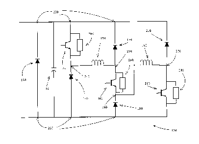
[0018] Part of the circuit 40 is the circuit illustrated in
Figure 2. The circuit 100 has a capacitor 110, a
first diode 120, a first semiconductor switching
subsystem 130, a second diode 140, and a first
inductor 150. The circuit 100 also has a second
semiconductor switching subsystem 160, a third diode
170, a second inductor 180 and a fourth diode 190.
- 13 -
CA 02845438 2014-03-12
Attorney Docket No. 1123P002W001
Finally, the circuit 100 has a fifth diode 200 and a
third semiconductor switching subsystem 210.
[0019] In the circuit 100, the diode 120 is coupled between
the input nodes 220, 230. Capacitor 110 is also
coupled between nodes 220, 230. The collector of the
first semiconductor switching subsystem 130 is coupled
to node 220 while the emitter of this first
semiconductor switching subsystem 130 is coupled to
node 240. Diode 140 is coupled between node 240 and
node 210. First inductor 150 is coupled between node
240 and node 250. The collector of the second
semiconductor switching subsystem is coupled to node
250 while diode 170 is coupled between node 250 and
node 220. The emitter of the second semiconductor
switching subsystem 160 is coupled to node 260 and
diode 190 is coupled between node 260 and node 230.
Second inductor 180 is coupled between node 260 and
node 270. Diode 200 is coupled between node 220 and
node 270. The collector of the third semiconductor
switching subsystem 210 is coupled to node 270 while
the emitter of the third semiconductor switching
subsystem 210 is coupled to the node 230.
[0020] In one implementation of the circuit 100, all the
semiconductor switching subsystems are commonly gated
or are controlled by a common gating signal. This
means that all the semiconductor switching subsystems
are simultaneously active or inactive. All the
semiconductor switching subsystems can thus be
activated or deactivated with a single signal.
- 14 -
CA 02845438 2014-03-12
Attorney Docket No. 1123P002W001
[0021] It should be noted that each semiconductor switching
subsystem may be equipped with an anti-parallel diode
280 coupled between each semiconductor switching
subsystem's collector and emitter.
[0022] As is well-known in the electronic arts, semiconductor
switching devices are "active" when they are
conducting and "non-active" or "inactive" when they
are not conducting. In more detail, semiconductor
devices, especially transistors, conduct across their
collector and emitter nodes depending on the voltage
applied to their gate node (i.e., control signal).
When a semiconductor switching device is conducting,
the device is considered "active". When a
semiconductor switching device is not conducting
across its collector and emitter nodes, the device is
considered "non-active" or "inactive" or
"deactivated".
[0023] Also in the circuit, the capacitor 110 operates as an
energy storage device which discharges its energy to
the inductors 150, 180. To generate the
electromagnetic pulses required for TMS or most forms
of magnetic stimulation, the capacitor has to charge
and discharge repeatedly. The duration of the
discharges is usually in the order of micro-seconds.
The pulses may be repeated at frequencies between 1 to
1000 Hz.
[0024] In circuit 100, input nodes 220, 230 are coupled to a
power source from which the capacitor 110 is charged.
To discharge the energy of capacitor 110 into
- 15 -
CA 02845438 2014-03-12
Attorney Docket No. 1123P002W001
inductors 150, 180, all the semiconductor switching
subsystems are active, thereby allowing current to
pass through the inductors 150, 180. Once the pulse
is done, all the semiconductor switching subsystems
are deactivated or rendered inactive simultaneously.
This causes the current within each inductor 150, 180
to be zero (i.e. very small). Normally, a single
inductor with an inductance equal to the combined
inductances of the first and second inductors would
require a certain amount of time in which to dissipate
its current after the single inductor has been
disconnected from a circuit. By splitting the
inductance into two separate inductors and
simultaneously disconnecting both inductors, each
inductor can dissipate its current independently and
separately from the other. Accordingly, the effective
amount of time required to dissipate the current from
the two separate inductors is less than the amount of
time required to dissipate the current from a single
inductor with the same inductance as the two
inductors. This is because, instead of having to
dissipate current from a single inductor, each
separate inductor dissipates its current in parallel
(yet separately) with the other inductor.
[0025] It should be noted that when all the semiconductor
switching subsystems are active, the two inductors
150, 180 operate as a single, combined inductance.
However, when the semiconductor switching subsystems
become inactive, each of the two inductors 150, 180
operates as an independent inductor.
- 16 -
CA 02845438 2014-03-12
Attorney Docket No. 1123P002W001
[0026] It is preferred that the semiconductor switching
subsystems are implemented as insulated gate bipolar
transistors (IGBTs). While not ideal, MOSFETs may
also be used as semiconductor switching devices.
Diodes are used throughout the circuit 100 as recovery
circuit elements. Again, while not ideal, thyristors
may also be used in place of the diodes in Figure 2.
[0027] In one implementation, one of the inductors (the first
inductor) operates as the coil 50 while the other
inductor may be located physically remote from the
coil 50. One of the inductors may thus be adjacent to
a patient's skull during treatment while the other
inductor is located with the rest of the TMS circuitry
and apparatus.
[0028] Regarding the inductance of the first and second
inductors, it is preferred that their inductances are
not equal. In fact, it is preferred that their
inductances be at a ratio of between 1:10 to 1:20 to
each other. For clarity, the inductance of the first
inductor is preferred to be 1/10th to 1/20th of the
inductance of the second inductor.
[0029] In operation, the circuit is coupled to a power
source. The capacitor is charged and, once charged,
is discharged into the two inductors. This discharge
is done when the semiconductor switching subsystems
are active. The current in the inductors is used to
create a magnetic field that is applied to the
patient's skull. After the magnetic field has been
applied, all the semiconductor switching subsystems
- 17 -
CA 02845438 2014-03-12
Attorney Docket No. 1123P002W001
are deactivated, thereby electronically isolating the
two inductors from the circuit. Each inductor then
independently dissipates its stored energy. The
process can then repeat for each electromagnetic pulse
needed for patient treatment.
[0030] It should be noted that while Figure 2 and the
description above discusses two inductors in the
circuit, other variants are, of course, possible.
Systems which use three or more inductors, with an
attendant increase in the number of semiconductor
switching subsystems, are possible. In these
variants, multiple inductors may be located adjacent
to the patient's skull. Similarly, multiple inductors
may be located as part of the circuit and may thus be
located remotely from the patient's skull.
[0031] In operation, the discharge of the capacitor causes a
current to pass through the inductors. The time
during which this is occurring can be termed the rise
time as energy is stored in each inductor's magnetic
field. During this time, the semiconductor switching
subsystems are active or activated. When the
capacitor's discharge is done, the semiconductor
switching subsystems are deactivated and the inductors
are isolated from the rest of the circuit. This
causes the energy in the inductors to be dissipated
with each inductor dissipating its energy
independently and separately from the other inductor
or inductors. This period of energy dissipation can
be termed the decay or recovery period as the energy
- 18 -
CA 02845438 2014-03-12
Attorney Docket No. 1123P002W001
stored in each inductor's magnetic field decays as the
inductor recovers from the capacitor's discharge.
[0032] For one implementation, as noted above, the first
inductor (acting as the treatment coil) has an
inductance that is 1/10 to 1/20 of the inductance in
the circuitry. For this configuration, the rise time
is extended and is, comparatively speaking, long. The
decay time for the small or first inductor is quite
small compared to the decay time for the large or
second inductor. The action potential or effective
electrical field induced in the patient's brain is
achieved during the decay time for the small inductor.
[0033] Referring to Figures 3 and 4, waveforms for the
circuit in operation are presented. Referring to
Figure 3, the waveform 300 for the gates in the
circuit are illustrated. Along with waveform 300, the
waveform 310 for the rise time of the inductors is
shown as well as the waveform 320 for the decay time
for the inductor 150 and the waveform 330 for the
decay time of the inductor 180.
[0034] As can be seen from Figure 3, the rise time of the
inductors 150, 180 is similar in duration and starts
once the switching subsystems are activated (see
waveform 310). Once the switching subsystems have
been deactivated, the decay time for inductor 150 is
much smaller than the decay time for inductor 180.
This can be seen by comparing waveform 320 with
waveform 330. Waveform 330 shows that the decay time
- 19 -
CA 02845438 2014-03-12
Attorney Docket No. 1123P002W001
for inductor 150 is but a fraction of the decay time
for inductor 180.
[0035] Referring to Figure 4, a much closer view of the
waveforms is presented. As can be seen, waveform 330
shows that the current in inductor 150 decays sharply
once the switching subsystem is deactivated (see
waveform 300). Conversely, the current in inductor
180 slowly decays after the switching subsystem is
deactivated (see waveform 320). Since there is no
confounding physiological effects after the current
decay from the smaller inductor 150, it is
advantageous to derive the action potential or
effective electrical field during the current decay
from the smaller inductor as the inductor discharges.
This is in contrast to current technology where the
action potential is derived from the rising time as an
inductor charges. In current technology, the benefits
from the action potential derived from the rising time
as an inductor charges is counteracted by the
physiological effects due to the long discharge time
of the inductor. By deriving the action potential
from the comparatively short decay time as the smaller
inductor discharges, the action potential is not
counteracted by physiological effects from a long
decay time.
[0036] It should be noted that current mono-phase technology
used in TMS applications have short rise times and
long decay times as the inductors used are rapidly
charged and then slowly discharged. The magnetic
- 20 -
CA 02845438 2014-03-12
Attorney Docket No. 1123P002W001
field induced by the charge and discharge of inductors
in current technology are similar in shape to the
charge/discharge waveform for the current in the
inductor -- these are characterized by short charging
times and long discharging times. The present
invention provides long charge times but very short
discharge times as the discharge times are determined
by the size of the inductors used. Since the magnetic
field produced by the smaller inductor is proportional
to the current in this smaller inductor and since the
electrical field induced by this magnetic field is
proportional to the magnetic field rate of change, the
electrical field has a narrow rectangular shape and is
proportional to the voltage across the device. This
narrow rectangular shape can be seen as part of
waveform 340 and can be seen in more detail in Figure
4. The electrical field produced by the magnetic
field in the mammalian tissue being treated is
therefore characterized as a short, sharp pulse which
mostly lasts only as long as the smaller inductor 150
(or the treatment inductor) is discharging or as long
as the current in the smaller inductor is decaying.
[0037] To assist in the above described system, a novel
system for positioning magnetic coils for TMS
treatment is also provided as part of the invention.
Current TMS methods are based on manual positioning of
these electromagnetic coils on the subject's head.
[0038] To determine where to place the magnetic coils, a
model of the subject's head is created. This is done
- 21 -
CA 02845438 2014-03-12
Attorney Docket No. 1123P002W001
by placing multiple fixed video cameras near the
subject's head and placing markers on the head. The
various views of the subject's head are then used to
create the model. Once the model has been created,
physicians can then determine where on the subject's
head should the electromagnetic coils be positioned.
Unfortunately, this process may be fraught with
inaccuracies as the subject may move his or her head
when the cameras are seeking to locate the markers on
the head.
[0039] Once the placement of the coils have been determined,
physically positioning these coils during treatment
can also be tricky. Currently, a physician or other
medical personnel will need to hold the coil in place
while the treatment is being administered. Given that
the coils can be quite heavy and that treatment can
last from seconds to minutes, this can be tiring and
thereby prone to errors. One alternative would be to
have a stationary holder for the coil as the treatment
progresses. Unfortunately, this is also fraught with
issues as the placement of the coil itself can be
problematic. The placement can only be as good as the
person locating the coil on the subject's head. This
person must, with the help of the model and the
physician's indication of where to place the coil,
locate that point on the subject's head and hold that
coil at that precise location while treatment is being
administered.
- 22 -
CA 02845438 2014-03-12
Attorney Docket No. 1123P002W001
[0040] In the novel coil placement system and method for
positioning electromagnetic coils relative to a
subject's head for transcranial magnetic stimulation,
a robotic arm is used with specific registration
points on the subject's head to construct a model of
the head. A user can position one end of the robotic
arm at each one of the multiple predetermined
registration points on the user's head and the
coordinates for this position is recorded. Once all
the coordinates for the registration points are
recorded, the system can generate a suitable reference
model for the head. The reference model for the
subject's head can then be used in conjunction with a
previously constructed treatment model which was used
for determining the subject's diagnosis and treatment
regimen. The reference model and the treatment model
can then be co-registered with each other so that
corresponding points on each model correspond with one
another. Thus, a point on the reference model's
forehead will register with the same point on the
treatment model.
[0041] The reference model can be used in multiple ways.
Once the reference model has been co-registered with
the treatment model, tracking the position of the
robot arm on the subject's head by way of the
reference model allows for easier placement of the
coil on the subject's head. By overlaying the
reference model with the treatment model, a user can
easily visualize the location of the treatment area.
Since the coordinate system on the reference model is
- 23 -
CA 02845438 2014-03-12
Attorney Docket No. 1123P002W001
known to the system, tracking the robot arm's position
on the reference model is simple and can be easily
displayed on the reference model. By highlighting the
designated treatment area on the treatment model and
overlaying the two models, a user can determine how
far or how close the robot arm is to the designated
treatment area. Positioning the robot arm precisely
at the designated treatment area can therefore be done
and, by attaching the coil to the end of the robot
arm, precise placement of the coil is thus now
possible.
[0042] The reference model can also be used in conjunction
with the robot arm for the actual treatment process.
Given the co-registration between the reference model
and the treatment model, the treatment area denoted on
the treatment model can be programmed into the
reference model after the co-registration. The robot
arm can then be programmed to position its end to the
coordinates of the treatment area. The robot arm can
also be programmed to remain at those coordinates for
a predetermined amount of time. By attaching a coil
to the robot arm, the robot can be used to deliver the
required treatment regimen to the subject.
[0043] In addition to the above, the reference model and the
robot arm can be used to deliver multiple treatment
regimens for multiple subjects. Each subject can have
his or her own reference and treatment models stored
in digital storage including the treatment model's
treatment area. A suitable program can then be used
- 24 -
CA 02845438 2014-03-12
Attorney Docket No. 1123P002W001
with a coil equipped robot arm to have the robot arm
deliver the required treatment regimen to the subject.
[0044] Referring to Figure 5, a block diagram of a system
which uses the present invention is illustrated. As
can be seen, the system 510 includes a control system
520, a robot arm 530, a TMS treatment subsystem 540,
and a treatment coil 550. A model construction
subsystem 560 is also present. The control system 520
controls the robot arm 530 and can determine the
coordinates in space for the end of the robot arm.
The control system 520 can also place and hold the end
of the robot arm at any suitable coordinate in space
reachable by the robot arm. The TMS treatment
subsystem includes the treatment coil 550 through
which magnetic fields can be projected. The model
construction system interfaces with the control system
to accept the coordinates entered into the control
system. The model construction system can create a
reference model of a subject's head based on
coordinates from the control system.
[0045] In operation, the user first has to register the
coordinates of specific registration points on the
subject's head. As an example, the user brings the
robot arm (either manually or by use of controls on
the control system) to the subject's forehead (at a
point between the eyebrows), to the crown of the
subject's head, to the back of the subject's neck (the
base of the skull), and to each of the subject's ears.
Alternatively, the robot arm can be brought to the
- 25 -
CA 02845438 2014-03-12
Attorney Docket No. 1123P002W001
left and right ears and the bridge of the nose as the
specific registration points. At each one of these
registration points, the user registers the
coordinates with the control system. This can be done
by the user manually registering the coordinates (i.e.
activating a button or switch on the control system).
Once the coordinates for all the registration points
have been entered, the model construction subsystem 60
can use these coordinates to constructed a reference
model of the subject's head. The construction of a
model of a subject's head given a number of reference
points on the subject's head is well-known in the art
and can be performed using off-the-shelf software.
[0046] It should be noted that the number and location of
these registration points are dependent on the
configuration of both the model construction subsystem
and the software used for constructing the reference
model. Other means for gathering the data from the
subject's head for the construction of the reference
model are, of course, possible. As an example,
instead of discrete registration points, the subsystem
may use a continuous listing of coordinates as the
user traces the outline of the subject's head using
the robot arm.
[0047] Once the model construction subsystem 560 has
constructed the reference model of the subject's head,
the reference model is then co-registered with the
treatment model. The treatment model is a pre-
existing model of a human head which is used by a
- 26 -
CA 02845438 2014-03-12
Attorney Docket No. 1123P002W001
physician in diagnosing the subject and in determining
the treatment locations on the subject's head. For
ease of reference, most physicians indicate the
treatment locations or areas on the treatment model.
[0048] To co-register the reference model with the treatment
model, multiple well-known methods can be used. As an
example, specific points which are on specific
features common to both models can be determined and
correlated on both models. Thus, as an example, the
point midway between the eyebrows, the crown of the
head, the location of the ears, and the base of the
back of the skull can be used as reference points. By
lining up these reference points on both models, the
two models can be co-registered with each other such
that corresponding points on the two models align with
each other. Of course, other methods for co-
registering the two models are possible and can be
used with the invention.
[0049] With the two models co-registered, a user can take
advantage of the co-registration to track the robot
arm's position relative to the subject's head. The
two models can be overlaid to one another so that the
treatment area can be seen on the reference model.
The location of the robot arm can then also be
illustrated on the reference model. As the user moves
the robot arm (whether manually or by using the
controls on the control system or by using a
preprogrammed movement pattern), the user can see how
far or how close the robot arm's end is to the
- 27 -
CA 02845438 2014-03-12
Attorney Docket No. 1123P002W001
treatment area. By attaching the coil to the end of
the robot arm, the coil's position relative to the
desired treatment area can now be viewed on the
overlaid models. A user can thus determine the amount
and direction of movement required by the robot arm to
place the coil in the treatment area.
[0050] The tracking of the robot arm's position and the
programmability of the robot arm can also be taken
advantage of by having the robot arm deliver the
treatment regimen to the subject. Once the two models
are co-registered, the coordinates for the treatment
area can be extracted from the treatment model. The
robot arm can therefore be programmed to position its
coil-equipped end at the treatment area for the amount
of time required by the treatment regimen. This
programmed behavior by the robot arm is repeatable and
can be used to deliver multiple instances of a
specific treatment regimen to a specific subject. The
specific subject's treatment model and reference model
can be stored in digital storage along with the
programmed steps required of the robot arm to deliver
the treatment regimen. When the subject returns for
subsequent treatment, the relevant models and
programming can be retrieved and used to treat the
subject.
[0051] It should be noted that some treatment regimens
require multiple treatment areas on the same subject.
For such regimens, it was previously thought that
multiple TMS machines were required, with each TMS
- 28 -
CA 02845438 2014-03-12
Attorney Docket No. 1123P002W001
machine treating a specific treatment area. However,
the use of the programmability characteristic of the
robot arm and the reference and treatment models
allows for a single TMS machine to deliver the same
treatment regimen as multiple machines. A robot arm
can be programmed to position the coil at one
treatment area for a given period of time and then
move to another treatment area for another period of
time. This can be repeated as many times as necessary
for as many treatment areas as possible for a single
subject.
[0052] Regarding the equipment to be used in the working of
the invention, the model construction subsystem can be
a suitable general purpose computing device with
suitable software for model construction. Of course,
this subsystem needs to be interfaced with the control
system for the robot arm so that the subsystem can
receive the relevant coordinates for the reference
points on the subject's head. The selection and use
of the model construction subsystem is well within the
skill set of a person skilled in the art.
[0053] It should be noted that the model construction
subsystem and the reference and treatment model
generator can be similar to the visor2TM product from
ANT Neuro (www.ant-neuro.com) in the Netherlands and
may use similar model construction subroutines and
algorithms. A software package similar to this
product may also be used for neuronavigation or for
- 29 -
CA 02845438 2014-03-12
Attorney Docket No. 1123P002W001
navigating either one of or both of the reference and
treatment models.
[0054] Regarding the robot arm, in one implementation, the
robot arm manufactured by KUKA Roboter GmbH as
Lightweight Robot 4 (LWR 4) was found to be suitable.
This product is a 7-axis jointed arm robot and can be
operated with position, velocity, and torque control.
Each of the joints has a position sensor on the input
side and position and torque sensors on the output
side. The Lightweight Robot 4 has five joint modules,
a base frame, and a 2-axis in-line wrist. Systems and
devices similar to this product and with capabilities
comparable to this product may be used to implement
the invention.
[0055] Referring to Figure 6, a flowchart detailing the steps
in a method according to one aspect of the invention
is illustrated. The process starts with step 600,
that of finding specific registration points on the
subject's head. This step may use predetermined
registration points (e.g. the subject's ears and
bridge of the nose) or arbitrary registration points
which, when taken together, define at least part of
the subject's cranium.
[0056] With the registration points found, step 610 gathers
the 3D (three dimensional) coordinates of these
various registration points. This can be done by
sequentially placing the end of the robot arm at each
of the registration points and then triggering the
control system to take note or store of the
- 30 -
CA 02845438 2014-03-12
Attorney Docket No. 1123P002W001
coordinates of the position for the end of the robot
arm. By storing the coordinates of the various
registration points, these coordinates can be the
basis of the reference model to be created.
[0057] Step 620 is that of creating the reference model. The
reference model is created based on the coordinates of
the various registration points on the subject's head.
Well known methods and algorithms for creating a
hemispheric model of the subject's head can be used
for this step.
[0058] After the reference model has been created, step 630
is that of co-registering the reference model with the
treatment model containing the data as to the
treatment areas for the particular subject. The
process of co-registering the reference model with the
treatment model involves matching corresponding points
from one model with points on the other model. The
models are then manipulated and aligned with one
another until points on one model align and match with
corresponding points on the other model.
[0059] When the two models are aligned and co-registered, the
images of both models can be overlaid one another to
present a single image to be used by the user. The
points of interest on each of the models can now be
seen in relation to other points of interest. As an
example, the treatment area shown on the treatment
model can now be viewed in relation to the position of
the robot arm's end shown on the reference model.
- 31 -
CA 02845438 2014-03-12
Attorney Docket No. 1123P002W001
[0060] To assist the user in determining a patient's readings
and vital signs for, among other things, preparing for
the use of the above systems, the present invention
also provides a novel sensor pad configuration.
Current technology only uses single sensor pads to
detect and measure bioelectric signals. These single
sensor pads can be difficult to place -- technicians
or physicians who have a detailed knowledge of anatomy
are usually required to position the sensor pads for
optimal bioelectric readings. Of course, such
professionals are not infallible and it is not unusual
for multiple attempts before a suitable signal can be
detected and measured. This requirement that a
physician attend to a task as mundane as the placement
of sensors on a subject's body can be seen as a very
inefficient use of available resources.
[0061] Also, while current technology allows for the use of
multiple single sensor pads to cover an area from
which bioelectric signals are to be detected and
measured, each sensor pad typically requires at least
one lead or line to the bioelectric detection
equipment. Multiple sensor pads can therefore lead
to a tangled mess of wires which can be confusing if
not dangerous to the subject and those operating the
equipment. The use of multiple sensor pads can also
lead to variations in signal due to the variation in
sensor pad spacings.
[0062] This aspect of the invention provides systems,
methods, and devices relating to the detection and
- 32 -
CA 02845438 2014-03-12
Attorney Docket No. 1123P002W001
gathering of data for bioelectric signals. A
disposable two-dimensional array of sensor pads is
provided. Each of the sensor pads in the array has a
backing with a sensor on a first side and a connection
coupler on a second side. The first side is coated
with a conductive gel and the sensor pad array is
adhesively attachable to a subject's skin. The
connection coupler is usable with various electrical
coupler systems such as those which use a snap-on
connector. The two-dimensional array has at least two
sensor pads lengthwise and at least two sensor pads
widthwise. The array may be used with a bioelectric
data gathering module. The module may be self-
contained and attachable to the sensor pad array. The
module may include storage on to which the data
relating to the detected and measured bioelectric
signals can be stored. Similarly, the module may work
with external equipment which can analyze and store
the data.
[0063] Referring to Figure 7, a top plan view of a pad
according to one aspect of the invention is
illustrated. Figure 8 is a bottom plan view of the
pad in Figure 7. Figure 8A is a side view of the pad
in Figure 7. The pad 710 is a two-dimensional array
of sensor pads. In Figure 7, the pad 710 has three
sensor pads in a lengthwise direction and three sensor
pads in a widthwise direction. The pad 710 in Figure
7 is a 3 x 3 configuration but the pad can be as small
as a 2 x 2 configuration. A rectangular configuration
as opposed to the square configuration in Figures 7
- 33 -
CA 02845438 2014-03-12
Attorney Docket No. 1123P002W001
and 8 is also possible. It should be clear that the
pad 710 in Figure 7 is a low density two-dimensional
array of sensor pads.
[0064] Each sensor pad 720A, 720B, 7200, 7201 has a first
side 730 and a second side 740. Each sensor pad 720A-
7201 has a sensor 750 on the first side and a
connection coupler 760 on the second side. The sensor
750 and connection coupler 760 are set on a flexible
backing 770. The sensor 750 may be a Ag-Ag/C1
(silver-silver chloride) sensor which is well-known to
the person skilled in the art. Other suitable sensors
may also be used. The
connection coupler illustrated
in the figures is a metallic conductor which is of a
snap-on type connector well-known to the person
skilled in the art. Other types of connectors may
also be used as the connection coupler. As an
alternative, instead of a single button snap
connector, the array may have a smaller electrical
interface. For such an option, instead of a single
connector per electrode, a single connector that
connects all the sensors to the external circuitry
could be used.
[0065] The first side of each sensor pad may be coated with a
conductive gel to assist in the sensor sensitivity to
the bioelectric signals. As well, at least part of
each sensor pad may also be coated with a suitable
adhesive so that the sensor pad may adhere to a
subject's skin.
- 34 -
CA 02845438 2014-03-12
Attorney Docket No. 1123P002W001
[0066] When in use, the pad 710 may be placed in the region
of where a bioelectric signal is to be measured or
detected. In one example, the electrical activity of
specific arm muscles may need to be measured. For
this example, the pad can be placed in the general
region of the desired muscle. As an example, the
bicep may be the muscle of interest. To use the pad,
the pad is placed in the general area of the bicep and
connectors are attached to each of the connection
couplers on the pad. The leads attached to the
connectors are then coupled to suitable bioelectric
measuring equipment. Since the signals are electric
potentials, each sensor's reading is taken relative to
a base and the reading from one of the sensors can be
taken as the base or a separate sensor attached
elsewhere on the subject's body can be used as the
base. Once the leads are connected to the connection
couplers, the various signals are detected and the
signals of interest can be isolated if desired.
[0067] Since the above example would require multiple leads
connected to the pad, potentially leading to a
confusion of wires, one alternative is for the
provision of a data gathering module. A block diagram
of such a data gathering module is illustrated in
Figure 9. The module 800 has a number of components
-- at least one A/D (analog/digital) converter 810, an
amplifier 820, and an external interface submodule
830. The A/D converter 810 converts analog signals to
digital signals while the amplifier 820 amplifies weak
signals. The data gathering module may be configured
- 35 -
CA 02845438 2014-03-12
Attorney Docket No. 1123P002W001
to directly couple to each of the connection couplers
on the pad. The data gathering module may be equipped
with multiple connector couplers, each of which may be
usable with the connection couplers on the pad. In
one configuration, the data gathering module is
equipped with a matrix or array of connection
couplers. The array of connection couplers can be
configured to directly match and mate with the
connector couplers on the pad. Alternatively, the
data gathering module may be equipped with a multi-
connection connector coupler that mates with or
couples with a suitable connector coupler on the pad.
For this alternative, instead of single couplers per
sensor, a single multi-connection connector coupler
can be used on the pad.
[0068] Depending on the configuration of the data gathering
module, the signal detected by each sensor pad on the
pad can be separately amplified and digitally
converted by the data gathering module. For such a
configuration, multiple instances of the A/D converter
and of the amplifier may be present. As an
alternative, a single high speed A/D converter and a
single amplifier may be used for all the different
multiplexed signals from the various sensor pads.
[0069] Regarding the external interface submodule, this
submodule is used for interfacing with equipment
external to the data gathering module. As an
example, the data gathering module can provide a
bridge between the pad and data processing equipment
- 36 -
CA 02845438 2014-03-12
Attorney Docket No. 1123P002W001
that can analyze the signals detected and measured by
the module. The module couples to all the connection
couplers, converts the signals from analog to digital,
amplifies these signals, and, using the external
interface submodule, passes the converted and
amplified signals to the data processing equipment.
[0070] It should be noted that the external interface module
can use a wired connection between the external
equipment and the data gathering module.
Alternatively, a wireless connection between the
external equipment and the data gathering module can
also be used. For this alternative, the submodule may
include circuitry for a wireless connection to the
external equipment using well-known and widely-
accepted communications protocols. As an example,
circuitry that allows for a Bluetooth connection
between the data gathering module and the external
equipment can be included in the submodule.
[0071] As yet another alternative, instead of
transmitting/transferring the digital data generated
by the data gathering module, the digital data can be
stored in storage media attached or coupled to the
data gathering module. For ease of use, the storage
media may be removably coupleable to the data
gathering module. A user can thus attach the pad to
the subject and then attach the data gathering module
to the pad. Once the data gathering module is
activated, bioelectric signals are detected by the
various sensor pads and these signals are converted
- 37 -
,
CA 02845438 2014-03-12
Attorney Docket No. 1123P002W001
and amplified by the A/D converter(s) and the
amplifier(s). The data generated can, depending on
the configuration, be transmitted to external
equipment or be stored in a storage medium attached to
the module. The storage medium can then be removed
and attached to the external equipment as necessary.
[0072] For ease of use, the data gathering module can be
configured to communicate with an application running
on common smartphones. In one implementation, a data
analysis application running on a portable computing
device (e.g. a smartphone, tablet computer, laptop
computer, etc.) communicates with the data gathering
module using a wireless communications link. The data
generated is passed to the application and is
analyzed, with the results being presented to the
user.
[0073] Regarding the manufacture of the above devices and
systems, it is preferred that the backing on the pad
be of a fabric-type backing. It is also preferred
that the pad be hypoallergenic and that the backing be
free of latex. It is further preferred that the pad
as a whole be disposable. The data gathering module
may be removably attachable to the pad. Once a pad
has been used, the pad can be disposed of and the data
gathering module be re-used with another pad. The use
of the pad can therefore be hygienic for
patient/subjects and convenient for medical personnel.
[0074] The pad and the data gathering module can be used in
various medical related fields such as Surface
- 38 -
CA 02845438 2014-03-12
Attorney Docket No. 1123P002W001
electromyography (sEMG), electrocardiography (ECG or
EKG), and electroencephalography (EEG).
[0075] The method steps of the invention may be embodied in
sets of executable machine code stored in a variety of
formats such as object code or source code. Such code
is described generically herein as programming code,
or a computer program for simplification. Clearly, the
executable machine code may be integrated with the
code of other programs, implemented as subroutines, by
external program calls or by other techniques as known
in the art.
[0076] The embodiments of the invention may be executed by a
computer processor or similar device programmed in the
manner of method steps, or may be executed by an
electronic system which is provided with means for
executing these steps. Similarly, an electronic memory
means such computer diskettes, CD-Roms, Random Access
Memory (RAM), Read Only Memory (ROM) or similar
computer software storage media known in the art, may
be programmed to execute such method steps. As well,
electronic signals representing these method steps may
also be transmitted via a communication network.
[0077] Embodiments of the invention may be implemented in any
conventional computer programming language For
example, preferred embodiments may be implemented in a
procedural programming language (e.g."C") or an object
oriented language (e.g."C++", "java", or "C#").
Alternative embodiments of the invention may be
implemented as pre-programmed hardware elements, other
- 39 -
CA 02845438 2014-03-12
Attorney Docket No. 1123P002W001
related components, or as a combination of hardware
and software components.
[0078] Embodiments can be implemented as a computer program
product for use with a computer system. Such
implementations may include a series of computer
instructions fixed either on a tangible medium, such
as a computer readable medium (e.g., a diskette, CD-
ROM, ROM, or fixed disk) or transmittable to a
computer system, via a modem or other interface
device, such as a communications adapter connected to
a network over a medium. The medium may be either a
tangible medium (e.g., optical or electrical
communications lines) or a medium implemented with
wireless techniques (e.g., microwave, infrared or
other transmission techniques). The series of computer
instructions embodies all or part of the functionality
previously described herein. Those skilled in the art
should appreciate that such computer instructions can
be written in a number of programming languages for
use with many computer architectures or operating
systems. Furthermore, such instructions may be stored
in any memory device, such as semiconductor, magnetic,
optical or other memory devices, and may be
transmitted using any communications technology, such
as optical, infrared, microwave, or other transmission
technologies. It is expected that such a computer
program product may be distributed as a removable
medium with accompanying printed or electronic
documentation (e.g., shrink wrapped software),
preloaded with a computer system (e.g., on system ROM
- 40 -
CA 02845438 2014-03-12
Attorney Docket No. 1123P002W001
or fixed disk), or distributed from a server over the
network (e.g., the Internet or World Wide Web). Of
course, some embodiments of the invention may be
implemented as a combination of both software (e.g., a
computer program product) and hardware. Still other
embodiments of the invention may be implemented as
entirely hardware, or entirely software (e.g., a
computer program product).
[0079] A person understanding this invention may now conceive
of alternative structures and embodiments or
variations of the above all of which are intended to
fall within the scope of the invention as defined in
the claims that follow.
- 41 -