Language selection

Search

Patent 2846679 Summary

Third-party information liability

Some of the information on this Web page has been provided by external sources. The Government of Canada is not responsible for the accuracy, reliability or currency of the information supplied by external sources. Users wishing to rely upon this information should consult directly with the source of the information. Content provided by external sources is not subject to official languages, privacy and accessibility requirements.

Claims and Abstract availability

Any discrepancies in the text and image of the Claims and Abstract are due to differing posting times. Text of the Claims and Abstract are posted:

  • At the time the application is open to public inspection;
  • At the time of issue of the patent (grant).
(12) Patent: (11) CA 2846679
(54) English Title: PLASMA SOURCE
(54) French Title: SOURCE DE PLASMA
Status: Granted
Bibliographic Data
(51) International Patent Classification (IPC):
  • H01J 37/32 (2006.01)
(72) Inventors :
  • KRASSNITZER, SIEGFRIED (Austria)
  • LENDI, DANIEL (Switzerland)
  • HAGMANN, JUERG (Switzerland)
(73) Owners :
  • OERLIKON SURFACE SOLUTIONS AG, PFAEFFIKON (Switzerland)
(71) Applicants :
  • OERLIKON TRADING AG, TRUBBACH (Switzerland)
(74) Agent: SMART & BIGGAR LP
(74) Associate agent:
(45) Issued: 2019-10-22
(86) PCT Filing Date: 2012-08-29
(87) Open to Public Inspection: 2013-03-14
Examination requested: 2017-06-02
Availability of licence: N/A
(25) Language of filing: English

Patent Cooperation Treaty (PCT): Yes
(86) PCT Filing Number: PCT/EP2012/003623
(87) International Publication Number: WO2013/034258
(85) National Entry: 2014-02-26

(30) Application Priority Data:
Application No. Country/Territory Date
10 2011 112 759.7 Germany 2011-09-08

Abstracts

English Abstract


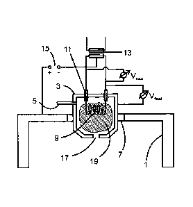
The present invention relates to a plasma source which is arranged in floating
fashion on a
vacuum chamber, wherein the plasma source comprises a source housing, and a
filament
is provided in the source housing and is arranged so as to be insulated
therefrom, wherein
means for measuring the potential drop between the source housing and the
filament are
provided. The measured potential drop can be used for regulating the voltage
heating the
filament. According to the invention, corresponding means are provided.


French Abstract

La présente invention concerne une source de plasma qui est disposée flottante sur une chambre à vide, la source de plasma comportant un boîtier et ledit boîtier abritant un filament qui disposé de manière isolée dudit boîtier, des moyens de mesure de la chute de potentiel étant prévus entre le boîtier et le filament. La chute de potentiel mesurée peut être utilisée pour la régulation de la tension chauffant le filament. Des moyens correspondants sont prévus selon l'invention.

Claims

Note: Claims are shown in the official language in which they were submitted.


5

CLAIMS:

1. Plasma source on a vacuum chamber for generating a plasma in the vacuum
chamber, wherein the plasma source comprises a source housing with an opening
protruding into the vacuum chamber and wherein, in the source housing, a
filament is
provided to which a heater voltage (V heiz or U heiz) can be applied to the
filament through
supply lines that pass through insulated via openings formed in the source
housing, so
that the filament can be heated by means of a current flow, wherein the source
housing
is placed on the vacuum chamber in a manner electrically insulated therefrom,
and in
that means are provided for measuring a potential drop (V float or U float)
between a supply
line to the filament and the source housing that represents the state of the
potential drop
between the filament and a plasma ignited inside the source housing, and thus
for the
state of the emission of electrons from the filament, and means are provided
for
regulating the heater voltage (V heiz or U heiz) that are configured to
process the measured
value of potential drop (V float or U float) as control signal in order to
adjust the state for the
electron emission to be maintained.
2. Device with a plurality of plasma sources according to claim 1, wherein the

plasma sources are surrounded respectively by at least one source coil and the
plasma
is distributed over a processing height through a combination of a magnetic
field of an
external coil and a magnetic field of the at least one source coil over the
processing
height.
3. Device according to claim 1, wherein the heater voltage is fed by means
of at
least one switched-mode power supply, wherein a discharge voltage (V disc or U
disc)
required for the discharge is applied centrally on a filament loop and
opposite the
filament in the plasma.
4. Method for generating a plasma in a vacuum chamber, the method
comprising:
placing a plasma source with a source housing and a filament in the source
housing on the vacuum chamber,
applying a heater voltage (V heiz or U heiz) to the filament to heat the
filament by
means of a current flow,


6

maintaining the source housing opposite the vacuum chamber and on a floating
potential,
measuring a potential drop (V float or U float) between a supply line to the
filament
and the source housing inside which a plasma is burning and
using the measured potential drop for regulating a heater voltage (V heiz or U
heiz)
applied to the filament,
wherein the heater voltage results in a current heating the filament and thus
in
an emission of electrons.
5. Method according to claim 4, wherein the heater voltage is regulated in
such a
manner that the potential drop between the source housing and the filament is
maintained constant.
6. Method according to claim 4, wherein the potential drop between the source
housing and the filament is maintained at values between 0V and -10V.
7. Method according to claim 4, wherein the floating potential comprises an
electrically floating manner.

Description

Note: Descriptions are shown in the official language in which they were submitted.


81777416
1
PLASMA SOURCE
FIELD
The present invention relates to a plasma source. The invention also relates
to a method
for generating plasma by means of a therm ionic discharge.
BACKGROUND
In this connection, a filament is heated by means of current, which results in
the emission
of electrons from the hot surface of the filament. The electron emission from
hot surfaces
follows the law first described by Richardson:
J=AGT2eT
where J is the emission current density, T is the temperature and W is the
work function of
the electrons.
If the surface of the filament reaches a temperature which is grater than
approx. 2900K for
tungsten, sufficient electrons are emitted from the surface so that with their
help, as soon
as they are sufficiently accelerated due to a voltage, argon gas is ionized to
such an
extend that plasma can be maintained.
According to the state of the art, the heating of the filament is achieved
over a constant
current strength. If an AC voltage is applied, a phase cut control allows the
effective value
of the current to be regulated. When operating under high temperatures, the
filament
material (e.g. tungsten) evaporates, which results in the wire diameter of the
filament being
reduced. Consequently, the resistance of the filament as defined by the wire
will increase.
If the heater current remains unchanged, a stronger heating will ensue and
thus an
accelerated evaporation of the filament material. Within a short time, this
results in a
melting through. Figure la shows the diameter of the filament depending on the
duration of
= operation at constant heater current. Accordingly, figure lb shows the
filament temperature
depending on the duration of operation at constant heater current. It can be
clearly seen
that after an initially constant reduction of the wire diameter, the filament
burns through
quickly (pinch-through effect).
CA 2846679 2018-10-15

81777416
2
SUMMARY
The present invention has the task of providing a method with which such a
fast burning
through can be avoided and thus the duration of operation, i.e. the filament's
service life, can
be increased.
During their experiments to increase the service life, the inventors have
noticed on the one
hand that at a temperature of the filament wire that is maintained constant,
the wire diameter
is reduced at a nearly constant rate. Figure 3 shows the evolution of the wire
diameter
depending on the duration of operation of the filament, at a constant
temperature and in
comparison with a measurement at constant current strength.
In their experiments, the inventors on the other hand have surprisingly
noticed that when
operating at a constant drop of potential between the filament and the plasma,
the
temperature of the filament remains nearly constant and the evaporation rate
even decreases
when the filament diameter decreases.
According to the invention, the filament is thus operated not at constant
current strength but
at constant voltage.
Some embodiments of the invention provide plasma source on a vacuum chamber
for
generating a plasma in the vacuum chamber, wherein the plasma source comprises
a source
housing with an opening protruding into the vacuum chamber and wherein, in the
source
housing, a filament is provided to which a heater voltage (Vhez or tit-lea)
can be applied to the
filament through supply lines that pass through insulated via openings formed
in the source
housing, so that the filament can be heated by means of a current flow,
wherein the source
housing is placed on the vacuum chamber in a manner electrically insulated
therefrom, and
in that means are provided for measuring a potential drop (Vfieet or Ufieet)
between a supply
line to the filament and the source housing that represents the state of the
potential drop
between the filament and a plasma ignited inside the source housing, and thus
for the state
of the emission of electrons from the filament, and means are provided for
regulating the
heater voltage (Vheiz or Uheiz) that are configured to process the measured
value of potential
drop (Vheat or Ufloat)1 as control signal in order to adjust the state for the
electron emission to be
maintained.
CA 2846679 2018-10-15

81777416
2a
Some embodiments of the invention provide method for generating a plasma in a
vacuum
chamber, the method comprising: placing a plasma source with a source housing
and a
filament in the source housing on the vacuum chamber, applying a heater
voltage (Vheiz
or Uheiz) to the filament to heat the filament by means of a current flow,
maintaining the
source housing opposite the vacuum chamber and on a floating potential,
measuring a
potential drop (Vfloai or Ufioat) between a supply line to the filament and
the source housing
inside which a plasma is burning and using the measured potential drop for
regulating a
heater voltage (Vheiz or Uheiz) applied to the filament, wherein the heater
voltage results in
a current heating the filament and thus in an emission of electrons.
BRIEF DESCRIPTION OF THE DRAWINGS
FIG. la shows the diameter of a filament depending on the duration of
operation at constant
heater current;
FIG. lb shows the filament temperature depending on the duration of operation
at constant
heater current;
FIG. 2 shows the evolution of the wire diameter depending on the duration of
operation of the
filament at constant temperature in comparison with a measurement at constant
current;
FIG. 3a shows filament temperature as a function of filament diameter;
FIG. 3b shows filament evaporation rate as a function of filament diameter;
FIG. 4 shows a plasma source according to the state of the art;
FIG. 5 shows a plasma source according to the invention; and
FIG. 6 shows a switch-mode power supply.
DETAILED DESCRIPTION
The invention will now be described in detail on the basis of the figures by
way of example.
Figure 4 shows a plasma source according to the state of the art, which is
placed on a
vacuum chamber 1. The plasma source comprises a source housing 3 with an inlet
5 for
argon gas. In the source housing 3, a filament 9 is provided that is connected
to a
CA 2846679 2018-10-15

81777416
2b
transformer 13 via openings 11 insulated from the source housing 3. The
filament 9 consists
in the example of a tungsten wire with a diameter of 2mm. The transformer is
operated in the
example with an AC voltage of 50Hz. A heater current of approx. 200A flows
through the
filament 9. If the surface of the filament 9 reaches a temperature greater
than 2900K, a
sufficient number of electrons are emitted from the filament surface which,
when a discharge
voltage is applied by means of a voltage source 15 between the vacuum chamber
15 and the
transformer 13, the argon gas flowing through the inlet 5 into the inside of
the source housing
3 can ionize. The ignition of the discharge occurs in the first moment over a
resistance that
connedts the source housing 3 with the mass (not shown).
CA 2846679 2018-10-15

CA 02846679 2014-02-26
3
W02013034258
If there are enough load carriers, the discharge current can also be lead
through the
opening 17 (also called "orifice") into the vacuum chamber 1.
According to the invention, the source housing as represented in figure 5,
electrically
insulated by means of the insulation 7, is arranged on the vacuum chamber 1
and the
voltage between the source housing 3 held in floating potential and the supply
line to the
filament 9 is measured. The filament 9 is heated through a current I. At the
filament, a
voltage Vheiz, which can be adjusted by means of the transformer 13, drops.
After the
source body 3 has been mounted in an electrically floating manner, the
inventive potential
measurement between the supply line designated as cathode and the source
housing can
be assessed as characteristic for the state of the potential drop between the
filament 9 and
plasma 19 ignited inside the source housing, and thus for the state of the
exit of electrons
from the filament. According to the invention, this state is maintained
essentially constant,
for example by regulating the heater voltage Uheiz. The measurement of Vfloat
thus enables
the optimum state for the electron emission to be maintained. In this manner,
the
temperature of the filament can be maintained at an optimum. Optimum in this
connection
means that at this temperature, the evaporation rate of the filament material
is acceptably
low, yet sufficiently high to ensure a sufficiently high emission of electrons
for maintaining
the plasma. This makes it possible to considerably increase the lifespan of
the filament, i.e.
its service life, as compared with the state of the art.
According to one embodiment of the present invention, plasma source
arrangements for
heating and plasma etching of substrates can include a plurality of plasma
sources that
function according to the principle of thermionic emission. The filaments of
the plasma
sources are heated through applied voltages, wherein according to the
invention the
applied voltages are regulated in such a manner that the voltage between the
filament and
the floating source housing achieves a preferably essentially constant value
between OV
and -10V.
Preferably, the heating takes place through a switched-mode power supply.
According to
th is embodiment, source coils are provided at the individual plasma sources.
The plasma

CA 02846679 2014-02-26
4
W02013034258
in the processing chamber is distributed over the processing height through
the
combination of the magnetic field of an external coil and of the magnetic
fields of the
source coils over the processing height. The processing chamber and/or a
floating
insulated anode can serve as discharge anode.
According to a further embodiment of the present invention, the transformer 13
is replaced
by a so-called switched-mode power supply 21, as represented in figure 6. Such
a
switched-mode power supply 21 comprises a ferrite core 23 around which
windings of a
primary coil 25 are wound (shown for only one part of the ferrite core),
whilst the supply
lines to the filament for example merely form a loop. According to the
invention, a ferrite
core is provided on both supply lines to the filament and the discharge
voltage VDise is
applied centrally on the side opposite the filament 9. In this manner, i.e. by
means of the
switched-mode power supply, a very small and compact plasma source can be
achieved.

Representative Drawing
A single figure which represents the drawing illustrating the invention.
Administrative Status

For a clearer understanding of the status of the application/patent presented on this page, the site Disclaimer , as well as the definitions for Patent , Administrative Status , Maintenance Fee  and Payment History  should be consulted.

Administrative Status

Title Date
Forecasted Issue Date 2019-10-22
(86) PCT Filing Date 2012-08-29
(87) PCT Publication Date 2013-03-14
(85) National Entry 2014-02-26
Examination Requested 2017-06-02
(45) Issued 2019-10-22

Abandonment History

There is no abandonment history.

Maintenance Fee

Last Payment of $263.14 was received on 2023-08-01


 Upcoming maintenance fee amounts

Description Date Amount
Next Payment if standard fee 2024-08-29 $347.00
Next Payment if small entity fee 2024-08-29 $125.00

Note : If the full payment has not been received on or before the date indicated, a further fee may be required which may be one of the following

  • the reinstatement fee;
  • the late payment fee; or
  • additional fee to reverse deemed expiry.

Patent fees are adjusted on the 1st of January every year. The amounts above are the current amounts if received by December 31 of the current year.
Please refer to the CIPO Patent Fees web page to see all current fee amounts.

Payment History

Fee Type Anniversary Year Due Date Amount Paid Paid Date
Application Fee $400.00 2014-02-26
Maintenance Fee - Application - New Act 2 2014-08-29 $100.00 2014-05-02
Registration of a document - section 124 $100.00 2015-02-27
Maintenance Fee - Application - New Act 3 2015-08-31 $100.00 2015-06-10
Maintenance Fee - Application - New Act 4 2016-08-29 $100.00 2016-05-13
Request for Examination $800.00 2017-06-02
Maintenance Fee - Application - New Act 5 2017-08-29 $200.00 2017-08-18
Maintenance Fee - Application - New Act 6 2018-08-29 $200.00 2018-08-21
Registration of a document - section 124 $100.00 2019-04-04
Maintenance Fee - Application - New Act 7 2019-08-29 $200.00 2019-06-14
Final Fee $300.00 2019-08-23
Maintenance Fee - Patent - New Act 8 2020-08-31 $200.00 2020-08-31
Maintenance Fee - Patent - New Act 9 2021-08-30 $204.00 2021-08-27
Maintenance Fee - Patent - New Act 10 2022-08-29 $254.49 2022-08-29
Maintenance Fee - Patent - New Act 11 2023-08-29 $263.14 2023-08-01
Owners on Record

Note: Records showing the ownership history in alphabetical order.

Current Owners on Record
OERLIKON SURFACE SOLUTIONS AG, PFAEFFIKON
Past Owners on Record
OERLIKON SURFACE SOLUTIONS AG, TRUBBACH
OERLIKON TRADING AG, TRUBBACH
Past Owners that do not appear in the "Owners on Record" listing will appear in other documentation within the application.
Documents

To view selected files, please enter reCAPTCHA code :


To view images, click a link in the Document Description column. To download the documents, select one or more checkboxes in the first column and then click the "Download Selected in PDF format (Zip Archive)" or the "Download Selected as Single PDF" button.

List of published and non-published patent-specific documents on the CPD .

If you have any difficulty accessing content, you can call the Client Service Centre at 1-866-997-1936 or send them an e-mail at CIPO Client Service Centre.


Document
Description 
Date
(yyyy-mm-dd) 
Number of pages   Size of Image (KB) 
Abstract 2014-02-26 1 15
Claims 2014-02-26 2 67
Drawings 2014-02-26 5 87
Description 2014-02-26 4 199
Representative Drawing 2014-02-26 1 9
Cover Page 2014-04-07 1 37
Request for Examination 2017-06-02 2 80
Examiner Requisition 2018-04-13 5 279
Maintenance Fee Payment 2018-08-21 1 60
Amendment 2018-10-15 10 404
Claims 2018-10-15 2 68
Description 2018-10-15 6 246
Abstract 2019-02-27 1 16
Final Fee 2019-08-23 2 60
Representative Drawing 2019-10-01 1 6
Cover Page 2019-10-01 1 35
PCT 2014-02-26 16 517
Assignment 2014-02-26 2 66
Assignment 2015-03-26 6 826
Correspondence 2015-01-15 2 55