Note: Descriptions are shown in the official language in which they were submitted.
CA 02847354 2014-02-28
WO 2013/066538 PCT/US2012/057711
1
CIRCUIT PROTECTION DEVICE
Field of the Invention
[0001] The present invention relates generally to circuit protection
devices and, more
particularly, to a device that suppresses transient current/voltage surges.
Background of the Invention
[0002] Many of today's highly sensitive electronic components, such as
computer and
computer-related equipment that are used in commercial and residential
applications contain
transient voltage surge suppression (TVSS) devices. These devices protect
sensitive andJor
expensive electronic circuits and components from damage from over-voltage
fault conditions.
Such transient voltage surge suppression systems are typically designed for
moderate fault
conditions expected in normal use. In this respect, such systems are designed
to suppress
relatively minor fault conditions, but are not designed to protect against
major over-voltage
conditions. Examples of major over-voltage conditions include those that may
occur from losing
the system neutral or ground termination, or from repetitive current pulses as
from lightning
strikes. Such major over-voltage conditions can have catastrophic effects on
sensitive electronic
circuits and components. To prevent such fault conditions from reaching and
damaging
electronic circuits, components and equipment, it has been known to utilize
larger voltage surge
suppression devices. These devices are typically deployed at a building's
incoming electrical
service power lines, or within a building's power distribution grid to control
power surges in the
electrical lines to the building, or in the electrical lines to specific
floors of the building. Such
voltage surge suppression devices typically include a plurality of metal-oxide
varistors (MOVs)
connected in parallel between a service power line and a ground or neutral
line, or between a
neutral line and a ground line.
[0003] MOVs are non-linear, electronic devices made of ceramic-like
materials
comprising zinc-oxide grains and a complex amorphous inner granular material.
Over a wide
range of current, the voltage remains within a narrow band commonly called the
varistor voltage.
A log-log plot of the instantaneous voltage in volts versus the instantaneous
current in amps
yields a nearly horizontal line. It is this unique current-voltage
characteristic that makes MOVs
CA 02847354 2014-02-28
WO 2013/066538 PCT/US2012/057711
2
ideal devices for protection of sensitive electronic circuits against
electrical surges, over-
voltages, faults or shorts.
[0004] When exposed to voltages exceeding their voltage value, MOVs
become highly
conductive devices that absorb and dissipate the energy related to the over-
voltage and
simultaneously limit dump current to a neutral line or ground plane. If an
over-voltage condition
is not discontinued, the MOVs will continue to overheat and can ultimately
fail catastrophically,
i.e., rupture or explode. Such catastrophic failure may destroy the sensitive
electronic equipment
and components in the vicinity of the MOVs. The destruction of electrical
equipment or
components in the electrical distribution system can disrupt power to
buildings or floors for
prolonged periods of time until such components are replaced or repaired.
Moreover, the failure
of the MOVs in a surge suppression system may allow the fault condition to
reach the sensitive
electronic equipment the system was designed to protect.
[0005] In U.S. Patent No. 6,040,971 to Martenson et al., entitled CIRCUIT
PROTECTION DEVICE, there is disclosed a voltage suppression device for
protecting an array
of metal oxide varistors in a surge suppression system. The device was
operable to drop offline
an entire array of MOVs in the event that a voltage surge reached a level
wherein one or more of
the MOVs in the array might catastrophically fail. In the disclosed device and
system, a trigger
MOV was designed to have a lower voltage rating than any of the MOVs in the
array. Thus, the
entire array would drop offline in the event that a surge condition exceeded
the voltage rating of
the trigger MOV. In some instances, however, it may be desirable to maintain
the array of
MOVs active and to drop offline only those MOVs sensing a voltage surge
exceeding the voltage
rating of that particular MOV.
[0006] U.S. Patent No. 6,256,183 to Mosesian et al. discloses a circuit
protection device
that drops offline when an MOV within the device senses a voltage surge
exceeding the voltage
rating of the MOV. Both of the foregoing devices are designed to be connected
between a
service line and a ground line or neutral line, or between a neutral line and
a ground line.
[0007] The present invention provides a circuit protection device and a
transient voltage
surge suppression system incorporated within a tubular casing for use in
protecting an electrical
system from catastrophic failure due to excessive over-voltage conditions or
repetitive fault
conditions along such line.
CA 02847354 2014-02-28
WO 2013/066538 PCT/US2012/057711
3
Summary of the Invention
[0008] In accordance with a preferred embodiment of the present
invention, there is
provided a disposable voltage suppression device for suppressing voltage
surges in an electrical
circuit. The device is comprised of a tubular casing formed of an electrically
insulating material.
A first conductive component is attached to a first end of the casing. A
second conductive
component is attached to a second end of the casing. A voltage sensitive
element is disposed
within the tubular casing. The voltage sensitive element has a first surface
and a second surface
and a predetermined voltage rating across the first and second surfaces. The
voltage sensitive
element increases in temperature as voltage applied across the first and
second surfaces exceeds
the voltage rating. A first terminal is electrically connected to the first
surface of the voltage
sensitive element and to the first conductive component. A thermal element is
electrically
connected to the second surface of the voltage sensitive element. The thermal
element is an
electrically conductive solid at room temperature and has a predetermined
softening temperature.
A second terminal is electrically connected to the second conductive
component. The second
terminal has a contact portion in electrical connection with the second
surface of the voltage
sensitive element. The voltage sensitive element senses a voltage drop between
the first
conductive element and the second conductive element. The second terminal is
maintained in
electrical contact with the voltage sensitive element by the thermal element
and is biased away
therefrom, wherein the second terminal moves away from electrical contact with
the voltage
sensitive element and breaks the electrical current path if an over-voltage
condition sensed by the
voltage sensitive element exceeds the voltage rating of the voltage sensitive
element and causes
the voltage sensitive element to heat the thermal element beyond its softening
point. An arc
shield is movable from a first position wherein the arc shield allows contact
between the contact
portion of the second terminal and the voltage sensitive element to a second
position wherein the
shield is disposed between the contact portion of the second terminal and the
voltage sensitive
element when the second terminal moves from electrical contact with the
voltage sensitive
element.
[0009] In accordance with another aspect of the present invention, there
is provided a
voltage suppression device for suppressing voltage surges in an electrical
circuit. The device is
CA 02847354 2014-02-28
WO 2013/066538 PCT/US2012/057711
4
comprised of a tubular casing formed of an electrically insulating material. A
first conductive
component is attached to a first end of the casing. A second conductive
component is attached to
a second end of the casing. A voltage sensitive element having a predetermined
voltage rating is
provided. The voltage sensitive element increases in temperature as voltage
applied across the
voltage sensitive element exceeds the voltage rating. Terminals are provided
for electrically
connecting the voltage sensitive element between the first conductive
component and the second
conductive component. A normally closed, thermal switch is comprised of one
end of one of the
terminals, a surface of the voltage sensitive element and a thermal element.
The one end of one
of the terminals is maintained in electrical contact with the surface of the
voltage sensitive
element by the thermal element. The thermal switch is electrically connected
in series with the
voltage sensitive element between one of the conductive components and the
voltage sensitive
element. The thermal switch is thermally coupled to the voltage sensitive
element wherein one
of the terminals moves from a normally closed position wherein the one of the
terminals is
maintained in electrical contact with the surface of the voltage sensitive
element to an open
position wherein the one of the terminals moves out of electrical contact with
the surface of the
voltage sensitive element to form a gap between the one of the terminals and
the voltage
sensitive element when the temperature of the voltage sensitive element
reaches a level causing
the thermal element to soften. The one of the terminals includes a contact
portion and a second
portion that extends away from the contact portion. A non-conductive barrier
is operable to
move into the gap when the one of the terminals moves to an open position. The
barrier prevents
line voltage surges from arcing between the one of the terminals and the
voltage sensitive
element. The second portion of the one of the terminals extends over at least
a portion of the
non-conductive barrier and bends toward the thermal element so that the
contact portion is held
by the thermal element until the thermal element begins to soften. The non-
conductive barrier is
biased toward the thermal element, but is constrained from movement toward the
thermal
element by contact with the second portion of the one of the terminals at a
location that is spaced
away from the contact portion, until the thermal element begins to soften.
[0010] In accordance with another aspect of the present invention, there
is provided a
voltage suppression device for suppressing voltage surges in an electrical
circuit. The device is
comprised of a tubular casing formed of an electrically insulating material. A
first conductive
CA 02847354 2014-02-28
WO 2013/066538 PCT/US2012/057711
component is attached to a first end of the casing. A second conductive
component is attached to
a second end of the casing. A voltage sensitive element is disposed within the
casing. The
voltage sensitive element has a first surface and a second surface and a
predetermined voltage
rating across the first and second surfaces. The voltage sensitive element
increases in
temperature as voltage applied across the first and second surfaces exceeds
the voltage rating. A
first terminal is electrically connected to the first surface of the voltage
sensitive element and the
first conductive component. A thermal element is electrically connected to the
second surface of
the voltage sensitive element. The thermal element is an electrically
conductive solid at room
temperature and has a predetermined softening temperature. A second terminal
is formed of a
spring metal that has one end in electrical connection with the second surface
of the voltage
sensitive element and another end connected to the second conductive
component. The voltage
sensitive element senses a voltage drop between the first conductive component
and the second
conductive component. The second terminal is bent from a normal and relaxed
configuration to
be maintained in contact with the voltage sensitive element by the thermal
element. The second
terminal is inherently biased away from the voltage sensitive element toward
the normal and
relaxed configuration, wherein the second terminal springs away from
electrical contact with the
voltage sensitive element which softens and breaks the electrical current path
if an over-voltage
condition sensed by the voltage sensitive element exceeds the voltage rating
of the voltage
sensitive element and causes the voltage sensitive element to heat the thermal
element beyond its
softening point. An arc shield is movable from a first position wherein the
arc shield allows
contact between the second terminal and the voltage sensitive element to a
second position
wherein the arc shield is disposed between the second terminal and the voltage
sensitive element
when the second terminal moves from electrical contact with the voltage
sensitive element. The
second terminal has a contact portion for making electrical contact with the
thermal element and
a second portion. The second portion extends through the path of the arc
shield and blocks the
movement of the arc shield until the thermal element reaches its softening
point.
[0011] It is an advantage of the present invention to provide a circuit
protection device to
protect sensitive circuit components and systems from current and voltage
surges.
[0012] It is another advantage of the present invention to provide a
circuit protection
device as described above to prevent catastrophic failure of a transient
voltage surge suppression
CA 02847354 2014-02-28
WO 2013/066538 PCT/US2012/057711
6
(TVSS) system within a circuit that may occur from repetitive circuit faults
or from a single fault
of excessive proportion.
[0013] A further advantage of the present invention is to provide a
circuit protection
device as described above that includes a current suppression device and a
voltage suppression
device.
[0014] Another advantage of the present invention is to provide a circuit
protection
device as described above for protecting a transient voltage surge suppression
system having
metal-oxide varistors (MOVs).
[0015] A still further advantage of the present invention is to provide a
circuit protection
device as described above that includes a metal-oxide varistor as a circuit-
breaking device.
[0016] A still further advantage of the present invention is to provide a
circuit protection
device as described above that is modular in design and easily replaceable in
a circuit line.
[0017] These and other advantages will become apparent from the following
description
of a preferred embodiment of the present invention taken together with the
accompanying
drawings.
Brief Description of the Drawings
[0018] The invention may take physical form in certain parts and
arrangement of parts, a
preferred embodiment of which will be described in detail in the specification
and illustrated in
the accompanying drawings which form a part hereof, and wherein:
[0019] FIG. 1 is a partially-sectioned, side elevation view of a fuse-
holder showing a
tubular, circuit protection device inserted partially therein.
[0020] FIG. 2 is a perspective view of a circuit protection device
according to a preferred
embodiment of the present invention, showing the circuit protection device
mounted in a DIN-
rail fuse holder;
[0021] FIG. 3 is a cross-sectional view of the circuit protection device
shown in FIG. 2,
showing the device in a normal operating condition;
[00221 FIG. 4 is a cross-sectional view of the circuit protection device
shown in FIG. 2,
showing the device after actuation by a fault condition;
CA 02847354 2014-02-28
WO 2013/066538 PCT/US2012/057711
7
[0023] FIG. 5 is an exploded, perspective view of the circuit protection
device, shown in
FIG. 2;
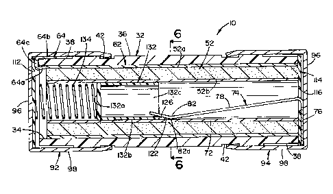
[0024] FIG. 6 is a cross-sectional view taken along lines 5-5 of FIG. 3;
[0025] FIG. 7 is a perspective view of a two-piece metal oxide varistor
element,
according to another embodiment of the present invention;
[0026] FIG. 8 is a cross-sectional view of a circuit protection device
having a "tripped-
circuit" indicator, illustrating another embodiment of the present invention;
and
[0027] FIG. 9 is a cross-sectional view showing the circuit protection
device of FIG. 8
showing the device in a "tripped-circuit" condition.
Detailed Description of Preferred Embodiment
[0028] Referring now to the drawings wherein the showings are for the
purpose of
illustrating a preferred embodiment of the invention only and not for the
purpose of limiting
same, FIG. 1 shows a circuit protection device 10, according to a preferred
embodiment of the
present invention, within a conventional, fuse holder 12.= Fuse holder 12, in
and of itself, forms
no part of the present invention, but shall be described briefly to illustrate
a preferred manner of
use of a circuit protection device 10.
[0029] Fuse holder 12 is comprised of a molded, polymer housing 14 having
leg portion
14a, 14b formed along the lower surface thereof. Leg portion 14a, 14b are
designed to allow
housing 14 to be attached, in snap-lock fashion to a mounting rail (not
shown), wherein spaced-
apart leads (not shown) that form part of an electrical circuit come into
electrical contact with
spaced-apart pairs of contact blades 24. A receiver 16 is pivotally mounted to
housing 14 by a
pin 17. Receiver 16 includes an elongated slot 16a that is dimensioned to
receive a cylindrical
fuse (not shown) or a circuit protection device 10 according to the present
invention.
[0030] Receiver 16 is pivotally movable to housing 14 and is movable bet
ween an
opened position, as shown in FIG. 1, and a closed position, wherein the ends
of a fuse or circuit
protection device 10 are in electrical contact with contact blades 24, as will
be better understood
from a further reading of the present specification.
[0031] In FIG. 2, circuit protection device 10 is shown mounted to a
conventional DIN-
rail fuse mount 20 having a base 22 and spaced-apart pairs of contact blades
24.
CA 02847354 2014-02-28
WO 2013/066538 PCT/US2012/057711
8
[0032] Circuit protection device 10 is generally comprised of a tubular,
insulated casing
32 that defines an inner bore or cavity 34. Bore or cavity 34 extends axially
through casing 32.
In the embodiment shown, casing 32 has a cylindrical shape and defines a
cylindrical, inner
cavity 34. Casing 32 has a predetermined wall thickness. In the embodiment
shown, cylindrical
tube casing 32 defines a cylindrical outer surface 36. The distal ends of
casing 32 are formed to
have two defined wall areas 38 of reduced thickness. Annular grooves or
recesses 42 are cut in
outer surface 36 of casing 32, as best seen in FIG. 5. These annular grooves
or recesses 42 are
spaced from wall areas 38 of reduced cross section.
[0033] Disposed within the casing is a voltage sensitive element (MOV) 52,
having an
outwardly facing, first surface 52a, and an inwardly facing, second surface
52b. In the
embodiment shown, the voltage sensitive element (MOV) 52 is tubular in shape,
wherein the
cylindrical outer surface of the voltage sensitive element (MOV) 52 defines
first surface 52a and
the cylindrical inner surface of voltage sensitive element (MOV) 52 defines
second surface 52b.
Voltage sensitive element (MOV) 52 is dimensioned to fit within casing 32.
Voltage sensitive
element (MOV) 52 has an axial length slightly less than the axial length of
casing 32, as shall be
described in greater detail below.
[0034] In accordance with the present invention, voltage sensitive element
(MOV) 52 is,
as its name implies, voltage sensitive and operable to heat up when a voltage
applied across the
device exceeds a preselected voltage. In accordance with the present
invention, voltage sensitive
element (MOV) 52 is preferably comprised of a metal-oxide varistor (MOV).
[0035] By way of background, metal oxide varistors (MOVs) are primarily
comprised of
zinc oxide granules that are sintered together. In the embodiment shown, the
zinc oxide granules
are sintered together to form a cylindrical tube. Zinc oxide, as a solid, is a
highly conductive
material. However, minute air gaps or grain boundaries exist between the
sintered zinc oxide
granules in an MOV, and these air gaps and grain boundaries inhibit current
flow at low voltage.
At higher voltages, the gaps and boundaries between the zinc oxide granules
are not wide enough
to block current flow, and thus the MOV becomes a highly conductive component.
This
conduction, however, generates significant heat energy in the MOV. MOVs are
typically
classified and identified by a "nominal voltage." The nominal voltage of an
MOV, typically
identified by VN(Dc), is the voltage at which the device changes from an "off
state" (i.e., the state
CA 02847354 2014-02-28
WO 2013/066538 PCT/US2012/057711
9
where the MOV is generally non-conductive) and enters its conductive mode of
operation.
Importantly, this voltage is characterized at the 1 mA point and has specified
minimum and
maximum voltage levels, referred to hereafter as VmiN and VtviAx respectively.
By way of
example, and not limitation, a metal-oxide varistor (MOV) having a nominal
varistor voltage,
VmDc), of 200 volts may actually exhibit a change from its generally non-
conductive to its
conductive state at a voltage between a minimum voltage, Vm1N, of 184 volts
and a maximum
voltage, VmAx, of 228 volts. This range of operating voltages for an MOV of a
rated nominal
voltage VN(DC) is the result of the nature of the device. In this respect, the
actual voltage value of
an MOV basically depends on the thickness of the MOV and on the number and
size of the zinc
oxide granules disposed between the two electrode surfaces. At the present
time, it is simply
impossible, because of the construction and composition of metal-oxide
varistors (MOVs), to
produce identical devices having identical operating characteristics.
[0036] Thus, although voltage sensitive element (MOV) 52 of circuit
protection device
preferably has a rated "nominal voltage" VN(Dc) at 1 mA, the actual voltage at
which the
MOV and every other MOV changes from a non-conducting state to a conducting
state may vary
between a VNAIN and a VmAx for the rated nominal voltage value. In the context
of the present
invention, the minimum voltage VmIN of the selected MOV is important, as will
be discussed in
greater detail below.
[00371 A second conductive lining 72 is provided to be in electrical
contact with second
surface 52b of voltage sensitive element (MOV) 52. In the embodiment shown,
second
conductive lining 72 is tubular in shape and is dimensioned to be positioned
adjacent to and in
contact with the inwardly facing, second surface 52b of voltage sensitive
element (MOV) 52.
Second conductive lining 72 is dimensioned such that at least a portion of
lining 72 extends
along the central portion of voltage sensitive element (MOV) 52. In the
embodiment shown,
second conductive lining 72 is cylindrical in shape and has a length at least
equal to the length of
voltage sensitive element (MOV) 52.
[0038] A first conductive liner 62 is disposed on first surface 52a of
voltage sensitive
element (MOV) 52. In the embodiment shown, first conductive liner 62 is
comprised of a
tubular element formed of a conductive material, such as metal. In a preferred
embodiment,
conductive liner 62 is formed of copper. In the embodiment shown, first
conductive liner 62 has
CA 02847354 2014-02-28
WO 2013/066538 PCT/US2012/057711
a length essentially equal to the length of voltage sensitive element (MOV)
52. First conductive
liner has an inner diameter that is dimensioned to closely match the outer
diameter of voltage
sensitive element (MOV) 52 such that the inner surface of first conductive
lining 62 is in
electrical contact with first surface 52a of voltage sensitive element (MOV)
52 whe n first
conductive lining 62 is positioned over voltage sensitive element (MOV) 52. A
first terminal 64
is electrically connected to first conductive lining 62. In the embodiment
shown, first terminal
64 is generally U-shaped. First terminal 64 is dimensioned to wrap around one
end of casing 32,
as best seen in FIGS. 3 and 4, with a leg portion 64a of U-shaped first
terminal 64 electrically
connected to first conductive lining 62 and another leg portion 64b overlaying
and extending
parallel to the outer surface of casing 32. As illustrated in FIGS. 3 and 4,
leg portion 64b is
disposed adjacent to wall area 38 at the end of casing 32 where the wall
thickness of casing 32 is
of reduced thickness. Leg portion 64a of U-shaped terminal 64 is bent inward
slightly toward
leg portion 64b to define a slightly flared or widened base portion 64c that
is slightly wider than
the thickness of wall area 38.
10039] Referring now to FIG. 5, a second terminal 74 is comprised of a
base portion 76
and an arm portion 78. In the embodiment shown, base portion 76 has a flat,
circular plate-like
configuration and arm portion 78 has an elongated, flat, rectangular strip-
like configuration. In a
normal configuration, arm portion 78 extends generally perpendicular from base
portion 76.
Base portion 76 and arm portion 78 are preferably integrally formed from a
rigid, electrically
conductive, flat, plate-like or sheet-like material. In a preferred
embodiment, second terminal
74, i.e., base portion 76 and arm portion 78, is formed from a copper plate.
The plate-like
material forming base portion 76 and arm portion 78 preferably has a thickness
such that arm
portion 78 is rigid, but the free end of arm portion 78 can move, i.e., be
deflexed, relative to base
portion 76 in a manner that shall be described in greater detail below.
10040] Base portion 76 has a diameter approximately equal to the diameter
of casing 32,
and arm portion 78 has a length wherein the free end thereof is located near
the axial center of
casing 32 when circuit protection device 10 is assembled.
[00411 As shown in the drawing, a bend 82 is formed in arm portion 78
near the free end
thereof. Bend 82 defines a contact point 82a to form an electrical connection
with inner surface
of second conductive liner 72, as shall be described in greater detail below.
CA 02847354 2014-02-28
WO 2013/066538 PCT/US2012/057711
11
[0042] Voltage sensitive elements (MOV) 52 with first and second
conductive liners 62,
72 are dimensioned to be disposed within casing 32 with the outer surface of
first conductive
lining 62 snuggly disposed against the inner surface of casing 32, as best
seen in FIGS. 3 and 4.
As shown in the drawings, in the embodiment shown, voltage sensitive element
(MOV) 52 and
first and second conductive linings 62, 72 have a length that is slightly
shorter than the length of
casing 32. U-shaped first terminal 64 is dimensioned to wrap around one end of
casing 32, with
leg portion 64b disposed along the outer surface of casing 32. Second terminal
74 is
dimensioned to be inserted in the other end of casing 32.
[0043] End caps 92, 94 are provided on the distal ends of casing 32 for
locking first and
second terminals within casing 32. Each cap 92, 94 is dimensioned to enclose
one end of casing
32. In this respect, each end cap 92, 94 is cup-shaped and has a circular base
wall portion 96 and
a cylindrical side wall portion 98. Caps 92, 94 are attached to casing 32 by
crimping the opened
end of side wall portions 98 onto casing 32. As best seen in FIGS. 3 and 4,
the open ends of side
wall portions 98 of caps 92, 94 are crimped, such that the free edge of side
wall portion 98 of
each cap 92, 94 is forced into an annular recess 42 formed on outer surface 36
of casing 32.
1100441 As best seen in FIG. 3, leg portion 64b of U-shaped first terminal
64 is captured
between wall area 38 of casing 32 and side wall portion 98 of end cap 92, such
that leg portion
64b of first terminal 64 is in electrical contact with metallic end cap 92. In
this respect, end cap
92 is in electrical contact with first surface 52a of voltage sensitive
element (MOV) 52 through
first terminal 64 and first conductive lining 62. An insulating disc 112 is
disposed within end
cap 92. As shown in the drawing, insulating disc 112 is dimensioned to be
disposed on the inner
surface of bottom wall portion 96. Insulating disc 112 is formed of an
electrically insulating
material and is provided basically to ensure end cap 92 is electrically
isolated from second
conductive lining 72.
[0045] As best seen in FIG. 4, base portion 64c of U-shaped first terminal
64 is enlarged
so as to secure the end of voltage sensitive element (MOV) 52, as well as
first conductive lining
62 that is disposed along the inner surface of voltage sensitive element (MOV)
52 spaced from
the end of casing 32. In other words, the ends of voltage sensitive element
(MOV) 52 and first
conductive lining 62 are spaced from first insulating disc 112 in the
embodiment shown.
CA 02847354 2014-02-28
WO 2013/066538 PCT/US2012/057711
12
[0046] Circular base portion 76 of second terminal 74 is dimensioned to
fit within cap
94, with base portion 76 disposed against, and in electrical contact with,
base wall portion 96 of
end cap 94.
100471 A second, insulating disc 114, formed from an insulating material,
is provided to
be positioned within end cap 94. Second insulating disc 114 is a flat disc
having a circular outer
edge that is dimensioned to fit within end cap 94. An aperture or hole 116 is
formed in the
center of insulating disc 114. Aperture 116 is dimensioned to allow arm
portion 78 of second
terminal 74 to extend therethrough. In this respect, insulating disc 114 is
designed to be
positioned adjacent the ends of casing 32, voltage sensitive element (MOV) 52,
and first and
second conductive linings 62, 72. Second insulating disc 114, essentially,
isolates the ends of
first and second conductive linings 62, 72 from base wall portion 96 of end
cap 94. Base portion
76 of second terminal 74 is confined between second insulating disc 114 and
bottom wall portion
96 of end cap 94, as best seen in FIGS. 3 and 4.
[0048] When second terminal 74 is initially assembled with casing 32, arm
portion 78 of
second terminal 74 extends axially into opening 34 defined within casing 32.
As best seen in
FIGS. 3 and 4, the free end of arm portion 78 of second terminal 74 is
slightly bent to define an
offset portion. Arm portion 78 of second terminal 74 is designed to be
displaced, i.e., forced,
from its normal, first position (as shown in FIG. 4) to a second position
wherein bend 82 formed
in arm portion 78, is brought into electrical contact with the inner surface
of second conductive
lining 72.
[0049] According to one aspect of the present invention, elongated arm
portion 78 of
second terminal 74 is held in the second position (shown in FIG. 3) in
electrical contact with the
inner surface of second conductive lining 72 by a thermal element 122. In a
preferred
embodiment, thermal element 122 is a solder material that has a relatively low
softening
temperature or melting temperature. A low melting temperature metal alloy or a
polymer having
a low softening temperature may be used. Thermal element 122 is preferably a
solid at room
temperature (25 C) and a solid up to a temperature around 35 C. Preferably,
thermal element
122 has a melting temperature or a softening temperature of between about 70 C
and 140 C and,
more preferably, has a melting temperature or softening temperature of between
90 C and about
100 C.
CA 02847354 2014-02-28
WO 2013/066538 PCT/US2012/057711
13
[0050] When attached to second conductive lining 72, as shown in FIG. 3,
arm portion
78 of second terminal 74 is elastically deformed (as contrasted with
plastically deformed) to
where arm portion 78 is held in place against the inner surface of second
conductive lining 72,
but would spring back to approximately its original, normal position, as shown
in FIG. 4, if not
restrained by thermal element 122. In other words, because arm portion 78 is
elongated and is
formed of a generally rigid metal material, it has a spring-like
characteristic. When secured in its
second position, as illustrated in FIG.3, a slot or recess 126 is formed
between the contact area of
arm portion 78 and the inner surface of second conductive lining 72.
[0051] A barrier element 132 is provided to be movable within casing 32.
As shall be
described in greater detail below, barrier element 132 is essentially an arc
shield. More
specifically, barrier element 132 is movable within second conductive lining
72. In the
embodiment shown, barrier element 132 is generally a cup-shaped device having
a flat circular
base 132a with a cylindrical side wall 132b. Barrier element 132 defines a
cylindrical irmer
cavity 132e. Cylindrical side wall 132b of barrier 132 is dimensioned such
that barrier 132 is
freely slidable within the opening defined by second conductive lining 72.
Barrier element 132
is preferably integrally formed of an electrically insulating, non-conductive
material, such as, by
way of example and not limitation, a polymer material. Biasing element 134
biases barrier
element 132 toward arm portion 78 of second terminal 74. When arm portion 78
is held against
the inner surface of second conductive lining 72 by thermal element 122, the
edge of side wall
132b of barrier element 132 is captured by recess or slot 126 formed by the
bent end of arm
portion 78 and the surface of second conductive lining 72. In the embodiment
shown, biasing
element 134 is a compression spring. Arm portion 78, barrier element 132, and
compression
spring 134 are dimensioned such that, when the free end of elongated arm 78 is
held against the
inner surface of second conductive lining 72, barrier element 132 is prevented
from movement
within second conductive lining 72 relative to arm portion 78 by bend 82 of
arm portion 78. As
shown in FIG. 3, compression spring 132 is compressed and exerts a biasing
force against base
132a of cup-shaped barrier 132 which is prevented from movement by bend 82 of
arm portion
78.
[0052] Referring now to the operation of circuit protection device 10, it
is contemplated
that one or more circuit protection devices 10 may be used together to protect
an electrical circuit
CA 02847354 2014-02-28
WO 2013/066538 PCT/US2012/057711
14
against a circuit fault condition. While circuit protection device 10 may be
used in a
conventional DIN-rail fuse mount 20, as shown in FIG. 2, circuit protection
device 10 is
preferably used in a fuse holder 12, as shown in FIG. 1. Fuse holder 12 allows
an individual to
easily connect a circuit protection device 10 to the electrical system or
circuit to be protected
without the individual being exposed to electrically energized power lines. In
other words, a
fuse holder 12 allows safe and easy attachment of a circuit protection device
10 to a "live"
circuit, as well as removal therefrom.
[0053] When circuit protection device 10 is disposed within holder 12,
and holder 12 is
in a closed position, caps 92, 94 of circuit protection device 10 are in
contact with contact blades
24 of holder 12. When holder 12 is attached across a power line and a ground
and neutral line of
an electrical circuit, a circuit path is created through circuit protection
device 10. More
specifically, a circuit path is created from end cap 92 through first
conductive lining 62 and
voltage sensitive element (MOV) 52 to second conductive lining 72. The circuit
path continues
from second conductive lining 72 through arm portion 78 of second terminal 74
(that is held in
contact with second conductive lining 72 by thermal element 122) to end cap
94. In other words,
when holder 12 is attached to a mounting rail (not shown) and circuit
protection device 10 is in
electrical contact with contact blades 24, a conductive path is defined
between a power line and a
ground or neutral line through circuit protection device 10. As will be
appreciated, a conductive
path will be established through circuit protection device 10 even if the
positions of end caps 92,
94 are reversed.
[0054] As indicated above, more than one circuit protection device 10 may
be used to
protect an electrical circuit. A circuit protection system may comprise "N"
number of circuit
protection devices 10 connected in parallel to a power line and ground or
neutral line. In such a
"multiple device system," each circuit protection device 10 has the same rated
"nominal voltage"
VN(jc) and a peak current surge rating. The total current surge protection
afforded by such a
multiple device system is thus approximately "N" times the peak current surge
rating of a circuit
protection device 10 used in the system. For example, if each circuit
protection device 10 has a
peak current surge rating of 10,000 amps, the assembly has a total peak
current surge rating of
(10,000 = N) amps. As indicated above, although each circuit protection device
10 may have the
same "rated nominal voltage," in actuality, the "rated nominal voltage" of
each of the MOVs
CA 02847354 2014-02-28
WO 2013/066538 PCT/US2012/057711
within a circuit protection device 10 may vary between a VmIN and a VmAx. As a
result, the
current surge experienced by each circuit protection device 10 may not occur
at the same instant,
as shall hereinafter be described.
[0055] In the event of an over-voltage condition or repetitive pulse
condition, the voltage
sensitive element (MOV) 52 of a circuit protection device 10 will experience
an over-voltage
condition. This over-voltage condition produces a voltage differential (bias)
between first
conductive lining 62 and second conductive lining 72 and across first surface
52a and second
surface 52b of voltage sensitive element (MOV) 52. When this occurs, thermal
energy is created
by the surge current, and each tubular voltage sensitive element (MOV) 52
begins absorbing
energy and dissipating such energy as heat. As the voltage differential across
a voltage sensitive
element (MOV) 52 becomes larger, electrical conductivity of the voltage
sensitive element
(MOV) 52 increases and increased amounts of heat are thereby generated. As
indicated above,
because the actual characteristics of each voltage sensitive element (MOV) 52
are not identical,
one voltage sensitive element (MOV) 52 in a series arrangement will have a
lower energy rating
and a faster thermal response time as contrasted to the others. Thus, various
voltage sensitive
elements (MOV) 52 will heat up more rapidly than other voltage sensitive
elements (MOV) 52
within a multiple device system. If the fault condition is severe enough, the
voltage sensitive
element (MOV) 52 of one or more circuit protection device 10 will heat up to
the melting
temperature of low temperature solder material of thermal element 122. When
this occurs, arm
portion 78 of second terminal 74 is no longer held in its first position (as
shown in FIG. 3).
When thermal element 122 melts, arm portion 78 is free to move away from inner
surface 52a of
voltage sensitive element (MOV) 52, as the metal material forming second
terminal 74 seeks =to
return to its normal planar configuration.
[0056] According to one aspect of the present invention, second surface
(the inner
surface) 52b of voltage sensitive element (MOV) 52 heats faster than first
surface (the outer
surface) 52a. This is due to second surface 52b having less surface area than
first surface area
52a, due to the different diameters of the respective surfaces. Because of its
smaller surface area,
the current density per unit area, and in turn, the joule heat per unit area,
is higher along second
surface 52b than along first surface 52a. The faster heating of second surface
52b provides
melting of thermal element 122 when fault conditions exist.
CA 02847354 2014-02-28
WO 2013/066538 PCT/US2012/057711
16
[0057] When arm portion 78 moves away from voltage sensitive element
(MOV) 52, the
conductive path through circuit protection device 10 is broken, wherein
circuit protection device
drops "off-line."
[0058] When one circuit protection device 10 drops "off-line," the
current surge rating
of the other circuit protection devices 10 in the multiple device system is
reduced. Using the
example set forth above, if one circuit protection device 10 drops "off-line,"
the system will lose
the 10,000 ampere surge capability, but would still have a current surge
rating of (10,000 = (N-1))
amps, until such time as the off-line circuit protection device 10 is
replaced.
[0059] The present invention thus provides a circuit protection device 10
that may be
used alone or in conjunction with other similar devices to form part of a
circuit protection
system. Circuit protection device 10 is a self-contained unit that is operable
to suppress voltage
spikes in a circuit and drop off-line when the voltage spike significantly
exceeds the rated
nominal voltage of the device to be protected thereby preventing catastrophic
failure of the same.
[0060] Referring now to FIGS. 8 and 9, a circuit protection device 210
illustrating an
ultimate embodiment of the present invention is shown. Circuit protection
device 210 in many
respects is the same as circuit protection device 10. In this respect,
components of circuit
protection device 210 that are like the components in circuit protection
device 10 are indicated
with the same reference numbers. The main difference between circuit
protection device 210
and the aforementioned circuit protection device 10 is that cylindrical
barrier element 132
includes an elongated pin 232 extending axially from flat, circular base 132a
of barrier element
132. Pin 232 is dimensioned to extend through an opening 234 formed through
first insulating
disk 112 and base wall portion 96 of end cap 92 when barrier element 132 is
maintained in the
first position against biasing element 134 by arm portion 78 of second
terminal 74, as best seen
FIG. 8. As shown in FIG. 8, end portion 232a of pin 232 extends beyond base
wall portion 96 of
end cap 92 when circuit protection device 210 is in its normal operating
configuration. In the
event of a fault condition that would cause circuit protection device 210 to
"trip," end portion
232a of pin 232 would be withdrawn into the inner bore 34 of casing 32 as
biasing element 134
forces barrier element 132 to a "tripped position." Thus, the absence of the
end portion 232a of
pin 232 extending from end cap 92 is an indication that circuit protection
device 210 has
"tripped" and should be replaced. Circuit protection device 210 thus provides
a quick and simple
CA 02847354 2015-05-22
=
17
configuration to provide an indicator means indicating the condition of
circuit protection device
210.
[0061]
The foregoing description is a specific embodiment of the present invention.
It
should be appreciated that this embodiment is described for purposes of
illustration only, and
that numerous alterations and modifications may be practiced by those skilled
in the art without
departing from the example embodiment of the invention described herein and
illustrated in the
drawings. For example, in the embodiment described heretofore, voltage
sensitive element
(MOV) 52 is a one-piece component. FIG. 7 shows a voltage sensitive element
152 formed of
two sections 154, 156 that may be used in place of voltage sensitive element
(MOV) 52 in circuit
protection device 10. As will be appreciated by those skilled in the art,
first and second
conductive linings 62, 72 would maintain sections 154, 156 in the desired
tubular configuration
within circuit protection device 10.