Note: Descriptions are shown in the official language in which they were submitted.
CA 02847979 2014-04-02
DC/DC CONVERTERS
Field of the Invention
The invention relates to the field of DC/DC converters.
Background
Bipolar or midpoint grounded DC systems have advantage with respect to
negative grounded
systems or floating systems, including but not limited to relatively low fault
currents during
ground faults, relatively low [and safe] potentials to ground and relatively
simple and
inexpensive instrumentation requirements. This is because the voltage with
respect to ground
is known and only half of what it would be with a negative grounded system.
Bipolar systems
also allow for the possibility of loads (or sources) distributed and operating
at two different
voltages. Accordingly, DC/DC converters, capable of transferring power between
two sources
grounded at the midpoint, are attractive in emerging applications such as
alternative energy
systems, energy storage and DC microgrids; a circuit of this type is shown in
FIG. 1. This circuit
uses four active switches and has some cost and complication associated with
the gating circuit.
Summary of the Invention
Forming one aspect of the invention is a method for transferring power between
two DC circuits,
each circuit being bipolar or connected at the midpoint thereof. The method
comprises the
steps of:
= coupling the high voltage bus across a pair of inductors, arranged in
parallel;
= coupling the low voltage bus across the pair of inductors;
= coupling the high voltage bus, the low voltage bus and the inductors by
active switches and
diodes, to provide for: a storage configuration, wherein energy is transferred
from one of the
buses and stored in the inductors; and a release configuration, wherein energy
is released
from the inductors and transferred to the other of the buses via a
freewheeling path through
one of the diodes.
1
CA 02847979 2014-04-02
Brief Description of the Drawings
FIG. 1 is a view of a bidirectional DC/DC converter for bipolar input and
output;
FIG. 2. is a view of a DC/DC converter for bipolar input and output circuits
that forms an
exemplary embodiment of the invention;
FIG. 3 is a PSIM model of the circuit of FIG. 2;
FIG. 4 is a PSIM model of the circuit of FIG. 1;
FIG. 5 is a plot of current vs. time created by the model of FIG. 3;
FIG. 6 is a similar to FIG. 5 of the circuit of FIG. 1;
FIG. 7 is a plot of voltage vs. time showing the reset function of the circuit
of FIG 3;
FIG. 8 is a view, similar to FIG. 3, showing a capacitor placed intermediate
the two midpoints;
FIG. 9 is a plot, similar to FIG. 7, but with a 114F capacitor placed
intermediate the two
midpoints;
FIG. 10 is a buck converter embodiment of the invention; and
FIG. 11 is a boost converter embodiment of the invention.
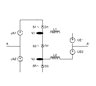
Detailed Description
A topology according to the first exemplary embodiment of the invention is
shown in FIG. 2 and
will be understood to be capable of providing bi-directional power flow
between two sources,
where both sources are connected at the mid-point.
The circuit operates with the voltage UA always higher that UE and for the
correct operation, S1
and S3 should have the same gating pattern while S2 has the complementary
gating signal.
2
CA 02847979 2014-04-02
A represents the midpoint of the high voltage bus; A' represents the midpoint
for the low voltage
bus. Although in many applications the common midpoint connection would be
grounded, it can
be connected to some other potential without affecting the circuit
performance.
Operation of the Circuit to Transfer Power from Up to UE
When Si and S3 are on, energy is transferred from Up to UE and stored in both
inductors.
When Si and S3 are turned off, the diode in anti-parallel with S2 provides a
free-wheeling path
for the inductor current. Although not shown, the duty cycle for the switches
will be understood
to be adjusted by a controller, equivalent to the controller for a half bridge
converter as function
of the voltage sources Up and UE
Operation of the Circuit to Transfer from UE
When S2 is closed, energy is transferred from UE to both inductors and stored.
When S2 is
turned off, the two diodes in anti-parallel with S3 and S4 provide a free-
wheeling path for the
current circulating on the inductor such that energy is now transferred from
UE plus both
inductors into Up. It will be understood by persons of ordinary skill that, in
application, additional
components [not shown] will be deployed to ensure correct operation of the
converter, including
but not limited to filter capacitors, sensors and gate drivers.
Advantages
The proposed topology reduces one active switch, increases the efficiency, and
reduces
complexity with respect to the half bridge circuit in FIG. 1.
Further, although in theory the same control signal can be provided to Si and
S4 and to S2 and
S3 in FIG. 1, in practice there are always differences in the magnitude of Um
and Up2 or UE1 and
UE2 or in the value of the inductances or parasitic components on the circuit.
Consequently the
positive and negative sections of the circuit would not be identical and they
would require
different operating points to work properly and to provide the required
control. Because of that
the circuit in FIG. 1 would have to be implemented with independent
controllers for the positive
and negative sections increasing the cost and complexity. In contrast, the
circuit in FIG. 2 is
able to operate with a single controller and having the exact same gating
signals to Si and S3.
3
CA 02847979 2014-04-02
The circuit will have an automatic "reset" action after S1 and S2 are turned
off which will ensure
the next cycle (closing of S1 and S3) is always started under the same
conditions (inductor
current) for the top and bottom circuit. This reset action transfers energy
from one of the
inductors to the other and/or to the sources and reduces the effect of
differences in inductance
values, split sources, or parasitic components in the circuit.
Furthermore, the "reset" effect has a self balancing action in some operating
conditions that is
beneficial to balance the DC-links (on either side of the converter). For
example if Um is slightly
higher than UA2, when S1 and S3 are turned off, the current on the inductor
located on the
positive side will be higher than the current on the inductor located on the
negative side of the
circuit. The difference in energy between inductor will be fed back to UA2
(through the diode in
anti-parallel with S3) and Up helping to balance the voltages Um and UA2, this
is achieved
without the need for a second controller.
The balancing effect mentioned above can be optimized and generalized by
adding an energy
storage component such as a capacitor in the path joining A with A' such that
this components
carries the voltage needed to compensate for unbalances in the circuit.
The balancing can also be optimized by using L1 and L2 as coupled inductors to
transfer power
between the upper and lower circuit as required.
On the other hand, if A and A' are connected, the circulating current in the
common connection
joining the mid-points of the two sources (A-A') indicates the unbalance in
the circuits, and by
measuring this current is possible to draw conclusions about the conditions
and health of the
sources and loads external to the DC/DC converter.
One conclusion that can be drawn from measuring the current flowing from A to
A' or the
voltage between A and A' (when a component is placed on that path) is to
identify possible
ground faults in the source circuits UA1, UA2, UE1, or UE2. This allows a
quicker detection of
the ground fault. Furthermore, if a passive component such as a capacitor is
placed in the path
joining A with A', it can automatically reduce the short circuit current
contribution from one or
several of the sources to ground faults in either of the source circuits
before the circuit is shut
down.
4
CA 02847979 2014-04-02
The circuit for the invention was modeled in PSIM and simulated to verify its
operation. The
model is shown in FIG. 3. In the simulation, a high voltage source (UAI and
UA2) +/- 400 VDC
is used while the low voltage source (UE1 and UE2) is +/- 200 VDC. The
switching frequency
for the converter is selected at 5 kHz and each of the two inductors is 5 mH.
The converter has
at the input and output general bi-directional voltage sources for simplicity,
but these sources in
practical applications could be batteries, DC generators, loads or other
elements of power
generation or consumption. The control is a single closed loop controller,
using the well known
PI control method, and regulating the current on the negative side of the low
voltage source. It
is clear that, depending on the application, the controller can regulate a
current measured in a
different part of the circuit or a voltage within the circuit with similar
results. The control is set to
produce currents of about 12 A in either direction for the low voltage side.
These parameters
and component values are only an example and represent values that could be
expected in a 5
kW DC/DC converter for battery applications. The results are completely
scalable to larger or
smaller power converters operated at the same or different voltage levels.
Different converters
would use different devices but the topology is applicable to the full range
of powers.
The circuit is compared with the dual half bridge circuit as shown in FIG. 1.
The dual half bridge
circuit was also modelled and simulated in PSIM and the model is shown in FIG.
4. Note that
the same single controller from FIG. 3 is used in the circuit of FIG. 4 also
controlling the
negative current.
A simulation was carried out to verify the operation of the two circuits with
a small unbalance
where UE1 is larger than UE2.
FIG. 5 shows the current through the inductor for the circuit of the invention
with UE1 20%
higher than UE2. Note that both currents (II and 12) are almost identical
although the controller
is only measuring one of them. The circuit self regulates the two currents
simultaneously with
knowledge of only one of them.
FIG. 6 shows the result of the same simulation for the circuit in FIG. 3. This
time the UE1 is
only 5% higher than UE2, but the current in the positive branch inductor,
which is not measured,
goes out of control. The circuit in FIG. 4 would only operate with one
controller and one
feedback signal if the components on the positive and negative sides are
identical. This is not
achievable in practice.
CA 02847979 2014-04-02
FIG. 7 shows the "reset" function of the circuit in FIG. 3 that allows is
balanced operation with a
single controller. In this simulation, the inductance in the positive circuit
is 20% higher than the
inductance in the negative circuit which is a considerable unbalance in the
circuit. The
description of the waveform is as follows:
= In every cycle, the ramping up of the current starts with the two
inductors having the
same current.
= During the ramping up of the current, S2 is off and SI and S3 are on.
= The larger inductance results in slower current rise for LI (II) such
that at the end of the
current rising phase the current on L1 is clearly lower than the current in
L2.
= At that point, the switches SI and S3 are turned off while S2 is turned
on.
= The circuit then has a short time while the current in LI continues
increasing while the
current in L2 decreases quickly. This is because one of the diodes (in this
case the
diode in anti-parallel with SI) turns on and energy is exchanged between the
inductors
through the high voltage source (UAI in this case).
= When the currents in both inductors are equal, the diode in anti-parallel
with SI turns off
and the circuit operates with the two inductors in series. This self-reset
function is what
allows controlling the current in both sub-circuits using one controller and
same
switching pattern to Si and S3.
Variations
Although the circuit of FIG. 3 is able to control the current positive and
negative with one
controller, the difference in waveforms shown in FIG. 7 as a result of
unbalances in the circuit
results in slightly different currents flowing between the positive sources
with respect to the
current flowing between the negative sources. This may not be desirable in
some applications
where there is no external balancing or regulation of the sources. To solve
this issue a
component such as a capacitor can be placed in between the two midpoint
references for the
sources as shown in FIG. 8. The capacitor would naturally take a voltage that
balances the
current flowing between the positive and negative sources.
FIG. 9 shows the same case for FIG. 7 but with a 1 uF capacitor placed between
the two mid-
points. The plot also includes the voltage across the capacitor. Note that now
the current in
both inductors are identical and a voltage of about 17 V appears across the
capacitor.
6
CA 02847979 2014-04-02
As another variation, by replacing the capacitor with a controllable voltage
source, it is possible
to adjust the difference in current flowing through the inductor that is not
directly controlled with
respect to the inductor that is directly controlled. If the voltage source can
be controlled to be
positive or negative, then the current on the upper circuit can be higher or
lower than the current
in the lower circuit. This is attractive in battery applications where the
positive and negative
battery banks are independent and it may be necessary to equalize the battery
banks with
different charges. The component between the two midpoints may be a simple
capacitor, a
battery, an ultracapacitor, an inductor or a more complex circuit able to
store some energy.
Because the current on the path between the two midpoints is small and the
voltage necessary
is only the amount of unbalance wanted in the circuit, the cost of the
balancing component is
low and its efficiency is high compared with the amount of power transferred.
The following table shows the result of simulations where the capacitor in
FIG. 8 was replaced
with a voltage source and how the current on the positive section of the
circuit is controlled with
the magnitude of this voltage.
Voltage between Current in Current in L2
midpoints L1
0 V 12.00 A 12.00 A
V 12.07A 12.00 A
20V 12.12A 12.00 A
-10 V 11.93 A 12.00 A
-20V 11.87 A 12.00 A
In practice, the voltage between the two midpoints can be controlled just by
adding a delay
(positive of negative) for switching off S1 with respect to S3. This can be
easily implemented on
a digital controller.
The circuit in FIG. 2 can be modified to satisfy other non-isolated
applications that use bipolar
inputs and outputs. One of them is a unidirectional buck only circuit that can
be used to transfer
power from a bipolar source to a bipolar load operating at a lower voltage.
The buck circuit is
shown in FIG. 10 where S2 has been removed from FIG. 2 to provide only
unidirectional power
flow.
7
CA 02847979 2014-04-02
The circuit can also be used in a unidirectional boost application where power
is transferred
from a bipolar source to a bipolar load operating at a higher voltage. The
boost circuit is shown
in FIG. 11 where Si, S3, and D2 have been removed from FIG. 2 to provide
unidirectional
power flow. In this case the circuit is shown with the midpoints grounded
although it is not
required.
Whereas several specific embodiments are herein shown and described, it will
be evident to
persons of ordinary skill that other variations are possible. Accordingly, the
invention should be
understood as limited only by the accompanying claims, purposively construed.
8