Note: Descriptions are shown in the official language in which they were submitted.
CA 02850073 2014-03-03
WO 2014/065904 PCT/US2013/049294
OPTICAL SOURCE DRIVER CIRCUIT FOR DEPTH IMAGER
Background
A number of different techniques are known for generating three-dimensional
(3D)
images of a spatial scene in real time. For example, 3D images of a spatial
scene may be
generated using triangulation based on multiple two-dimensional (2D) images.
However, a
significant drawback of such a technique is that it generally requires very
intensive
computations, and can therefore consume an excessive amount of the available
computational
resources of a computer or other processing device. Also, it can be difficult
to generate an
accurate 3D image under conditions involving insufficient ambient lighting
when using such a
technique.
Other known techniques include directly generating a 3D image using a depth
imager
such as a time of flight (ToF) camera. ToF cameras are usually compact,
provide rapid image
generation, and operate in the near-infrared part of the electromagnetic
spectrum. As a result,
ToF cameras are commonly used in machine vision applications such as gesture
recognition in
video gaming systems or other types of image processing systems implementing
gesture-based
human-machine interfaces. ToF cameras are also utilized in a wide variety of
other machine
vision applications, including, for example, face detection and singular or
multiple person
tracking.
A typical conventional ToF camera includes an optical source comprising, for
example,
one or more light-emitting diodes (LEDs) or laser diodes. Each such LED or
laser diode is
controlled to produce continuous wave (CW) output light having substantially
constant
frequency and amplitude. The output light illuminates a scene to be imaged and
is scattered or
reflected by objects in the scene. The resulting return light is detected and
utilized to create a
depth map or other type of 3D image. This more particularly involves, for
example, utilizing
phase differences between the output light and the return light to determine
distances to the
objects in the scene. Also, the amplitude of the return light is used to
determine intensity levels
for the image.
However, the use of CW output light in a ToF camera has a number of
significant
drawbacks. For example, the frequency of the CW output light unduly restricts
the maximum
unambiguous range of the camera. More particularly, the maximum unambiguous
range is
generally given by cl2f, where f is the frequency of the CW output light and c
is the speed of
light. The maximum unambiguous range can be extended by decreasing the
frequency f, but
this approach also decreases the measurement precision.
1
CA 02850073 2014-03-03
WO 2014/065904 PCT/US2013/049294
In addition, when utilizing CW output light, image quality degrades as the
length of an
integration time window is decreased. As a result, a ToF camera often cannot
support a frame
rate that is sufficiently high to track dynamic objects in the scene. On the
other hand, saturation
of image pixels is observed as the length of the integration time window is
increased.
Conventional ToF cameras based on CW light are generally unable to provide
suitable
optimization of the integration time window.
Summary
Embodiments of the invention provide, by way of example, optical source driver
circuits
for ToF cameras and other types of depth imagers.
In one embodiment, a depth imager comprises a driver circuit and an optical
source.
The driver circuit comprises a frequency control module and a controllable
oscillator having a
control input coupled to an output of the frequency control module. An output
of the
controllable oscillator is coupled to an input of the optical source, and a
driver signal provided
by the driver circuit to the optical source utilizing the controllable
oscillator varies in frequency
under control of the frequency control module in accordance with a designated
type of
frequency variation, such as a ramped or stepped frequency variation.
The driver circuit in a given embodiment may additionally or alternatively
comprise an
amplitude control module, such that a driver signal provided to the optical
source varies in
amplitude under control of the amplitude control module in accordance with a
designated type
of amplitude variation, such as a ramped or stepped amplitude variation.
Other embodiments of the invention include but are not limited to methods,
systems,
integrated circuits, and computer-readable media storing program code which
when executed
causes a processing device to execute a sequence of steps.
Brief Description of the Drawings
FIG. 1 is a block diagram of an image processing system comprising a depth
imager that
includes an optical source driver circuit in one embodiment.
FIG. 2 shows an embodiment of a portion of a depth imager comprising an
optical
source and an associated driver circuit implementing ramp-based frequency and
amplitude
control modules.
FIG. 3 shows another embodiment of a portion of a depth imager comprising an
optical
source and an associated driver circuit implementing step-based frequency and
amplitude
control modules.
2
CA 02850073 2014-03-03
WO 2014/065904 PCT/US2013/049294
FIG. 4A illustrates an exemplary driver signal with ramped frequency and
amplitude
generated by the driver circuit of FIG. 2.
FIG. 4B illustrates an exemplary driver signal with stepped frequency and
amplitude
generated by the driver circuit of FIG. 3.
FIG. 5 is a plot showing input-output response of the optical source of FIG. 2
responsive
to application of the drive signal of FIG. 4A.
Detailed Description
Embodiments of the invention will be illustrated herein in conjunction with
exemplary
image processing systems that include depth imagers having optical source
driver circuits
configured to provide at least one of frequency variation and amplitude
variation in a given
optical source driver signal. It should be understood, however, that
embodiments of the
invention are more generally applicable to any image processing system or
associated depth
imager in which it is desirable to provide improved quality for depth maps or
other types of 3D
images.
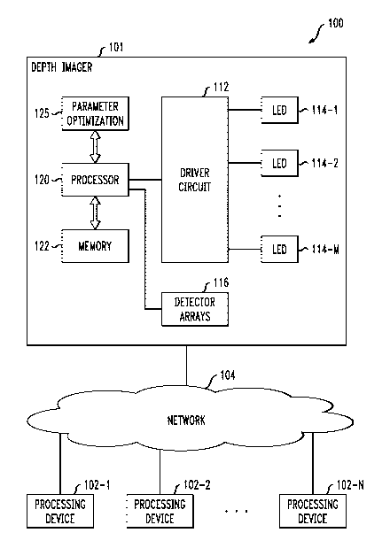
FIG. 1 shows an image processing system 100 in an embodiment of the invention.
The
image processing system 100 comprises a depth imager 101 that communicates
with a plurality
of processing devices 102-1, 102-2, . . . 102-N, over a network 104. The depth
imager 101 in
the present embodiment is assumed to comprise a 3D imager such as a ToF
camera, although
other types of depth imagers may be used in other embodiments. Such an imager
generates
depth maps or other depth images of a scene and communicates those images over
network 104
to one or more of the processing devices 102. Thus, the processing devices 102
may comprise
computers, servers or storage devices, in any combination. One or more such
devices also may
include, for example, display screens or other user interfaces that are
utilized to present images
generated by the depth imager 101.
Although shown as being separate from the processing devices 102 in the
present
embodiment, the depth imager 101 may be at least partially combined with one
or more of the
processing devices. Thus, for example, the depth imager 101 may be implemented
at least in
part using a given one of the processing devices 102. By way of example, a
computer may be
configured to incorporate depth imager 101.
In a given embodiment, the image processing system 100 is implemented as a
video
gaming system or other type of gesture-based system that generates images in
order to
recognize user gestures. The disclosed imaging techniques can be similarly
adapted for use in a
wide variety of other systems requiring a gesture-based human-machine
interface, and can also
3
CA 02850073 2014-03-03
WO 2014/065904 PCT/US2013/049294
be applied to numerous applications other than gesture recognition, such as
machine vision
systems involving face detection, person tracking or other techniques that
process depth images
from a depth imager.
The depth imager 101 as shown in FIG. 1 comprises a driver circuit 112 coupled
to a
plurality of optical sources 114-1, 114-2, . . . 114-M, illustratively
implemented as respective
LEDs, which may be arranged in an LED array. Although multiple optical sources
are used in
this embodiment, other embodiments may include only a single optical source.
Also, although
a single driver circuit 112 drives all of the optical sources 114 in this
embodiment, in other
embodiments each of the optical sources 114 may be driven by a separate driver
circuit 112. It
is to be appreciated that optical sources other than LEDs may be used. For
example, at least a
portion of the LEDs 114 may be replaced with laser diodes or other optical
sources in other
embodiments. More detailed examples of the driver circuit 112 will be
described below in
conjunction with FIGS. 2 and 1
The driver circuit 112 controls the LEDs 114 so as to generate output light
having
particular frequency and amplitude variations. Ramped and stepped examples of
such
variations provided by the driver circuit 112 can be seen in FIGS. 4A and 4B,
respectively. The
output light illuminates a scene to be imaged and the resulting return light
is detected using
detector arrays 116 and then further processed in depth imager 101 to create a
depth map or
other type of 3D image.
The driver circuit 112 in a given embodiment may comprise a frequency control
module, such that a driver signal provided to at least one of the LEDs 114
varies in frequency
under control of the frequency control module in accordance with a designated
type of
frequency variation, such as a ramped or stepped frequency variation.
The ramped or stepped frequency variation can be configured to provide, for
example,
an increasing frequency as a function of time, a decreasing frequency as a
function of time, or
combinations of increasing and decreasing frequency. Also, the increasing or
decreasing
frequency may follow a linear function or a non-linear function, or
combinations of linear and
non-linear functions.
In an embodiment with ramped frequency variation, a frequency control module
implemented in the driver circuit may be configured to permit user selection
of one or more
parameters of the ramped frequency variation including one or more of a start
frequency, an end
frequency and a duration for the ramped frequency variation.
Similarly, in an embodiment with stepped frequency variation, the frequency
control
module may be configured to permit user selection of one or more parameters of
the stepped
4
CA 02850073 2014-03-03
WO 2014/065904 PCT/US2013/049294
frequency variation including one or more of a start frequency, an end
frequency, a frequency
step size, a time step size and a duration for the stepped frequency
variation.
The driver circuit 112 in a given embodiment may additionally or alternatively
comprise
an amplitude control module, such that a driver signal provided to at least
one of the LEDs 114
varies in amplitude under control of the amplitude control module in
accordance with a
designated type of amplitude variation, such as a ramped or stepped amplitude
variation. Like
the ramped or stepped frequency variations noted above, the ramped or stepped
amplitude
variation can be configured to provide an increasing amplitude as a function
of time, a
decreasing amplitude as a function of time, or combinations of increasing and
decreasing
amplitude. Also, the increasing or decreasing amplitude may follow a linear
function or a non-
linear function, or combinations of linear and non-linear functions. Moreover,
the amplitude
variations may be synchronized with the frequency variations if the embodiment
includes both
an amplitude control module and a frequency control module.
In an embodiment with ramped amplitude variation, the amplitude control module
may
be configured to permit user selection of one or more parameters of the ramped
amplitude
variation including one or more of a start amplitude, an end amplitude, a bias
amplitude and a
duration for the ramped amplitude variation.
Similarly, in an embodiment with stepped amplitude variation, the amplitude
control
module may be configured to permit user selection of one or more parameters of
the stepped
amplitude variation including a one or more of a start amplitude, an end
amplitude, a bias
amplitude, an amplitude step size, a time step size and a duration for the
stepped amplitude
variation.
The driver circuit 112 can therefore be configured to generate driver signals
having
designated types of frequency and amplitude variations, in a manner that
provides significantly
improved performance in depth imager 101 relative to conventional depth
imagers. For
example, such an arrangement may be configured to allow particularly efficient
optimization of
not only driver signal frequency and amplitude, but also other parameters such
as an integration
time window.
The depth imager 101 in the present embodiment is assumed to be implemented
using at
least one processing device and comprises a processor 112 coupled to a memory
122. The
processor 120 controls the driver circuit 112 and detector arrays 116 using
software code stored
in memory 122.
The processor 120 may comprise, for example, a microprocessor, an application-
specific
integrated circuit (ASIC), a field-programmable gate array (FPGA), a central
processing unit
5
CA 02850073 2014-03-03
WO 2014/065904 PCT/US2013/049294
(CPU), an arithmetic logic unit (ALU), a digital signal processor (DSP), or
other similar
processing device component, as well as other types and arrangements of image
processing
circuitry, in any combination.
The memory 122 stores software code for execution by the processor 120 in
implementing portions of the functionality of depth imager 101, such as
portions of the
frequency and amplitude control modules described previously. A given such
memory that
stores software code for execution by a corresponding processor is an example
of what is more
generally referred to herein as a computer-readable medium or other type of
computer program
product having computer program code embodied therein, and may comprise, for
example,
electronic memory such as random access memory (RAM) or read-only memory
(ROM),
magnetic memory, optical memory, or other types of storage devices in any
combination. As
indicated above, the processor may comprise portions or combinations of a
microprocessor,
ASIC, FPGA, CPU, ALU, DSP or other image processing circuitry.
Also included in the depth imager 101 in the present embodiment is a parameter
optimization module 125 that is illustratively configured to optimize the
integration time
window of the depth imager as well as optimization of the frequency and
amplitude variations
for a given imaging operation. For example, the parameter optimization module
125 may be
configured to determine an appropriate set of parameters including integration
time window,
frequency variation and amplitude variation for the given imaging operation.
Such an arrangement allows the depth imager to be configured for optimal
performance
under a wide variety of different operating conditions, such as distance to
objects in the scene,
number and type of objects in the scene, and so on. Thus, for example,
integration time
window length of the depth imager 101 in the present embodiment can be
determined in
conjunction with selection of driver signal frequency and amplitude variations
in a manner that
optimizes overall performance under particular conditions. The parameter
optimization module
125 may be implemented at least in part in the form of software stored in
memory 122 and
executed by processor 120. It should be noted that terms such as "optimal" and
"optimization"
as used in this context are intended to be broadly construed, and do not
require minimization or
maximization of any particular performance measure.
The network 104 may comprise a wide area network (WAN) such as the Internet, a
local
area network (LAN), a cellular network, or any other type of network, as well
as combinations
of multiple networks. The depth imager 101 and each of the processing devices
102 may
incorporate transceivers or other network interface circuitry to allow these
devices to
communicate with one another over the network 104.
6
CA 02850073 2014-03-03
WO 2014/065904 PCT/US2013/049294
It should also be appreciated that embodiments of the invention may be
implemented in
the form of integrated circuits. In a given such integrated circuit
implementation, identical die
are typically formed in a repeated pattern on a surface of a semiconductor
wafer. Each die
includes at least one driver circuit and possibly other image processing
circuitry as described
herein, and may further include other structures or circuits. The individual
die are cut or diced
from the wafer, then packaged as an integrated circuit. One skilled in the art
would know how
to dice wafers and package die to produce integrated circuits. Integrated
circuits so
manufactured are considered embodiments of the invention.
The particular configuration of image processing system 100 as shown in FIG. 1
is
exemplary only, and the system 100 in other embodiments may include other
elements in
addition to or in place of those specifically shown, including one or more
elements of a type
commonly found in a conventional implementation of such a system.
FIG. 2 shows an embodiment of a portion 200 of a depth imager comprising an
optical
source 204, illustratively implemented as an LED, and an associated driver
circuit 202
configured to provide synchronized ramp-based frequency and amplitude
variations in imager
output light emitted by the optical source 204. The driver circuit 202 in this
embodiment
comprises a frequency control module 205, a voltage controlled oscillator 206
and an amplitude
control module 207. The voltage controlled oscillator 206 has a control input
coupled to an
output of the frequency control module 206 and its output is coupled to an
input of the optical
source 204 via a mixer 208.
The mixer 208 more particularly has a first input coupled to the output of the
voltage
controlled oscillator 206, a second input coupled to an output of the
amplitude control module
207, and an output providing the driver signal for the optical source 204. In
this embodiment,
the mixer 208 serves to provide a single driver signal that combines the
amplitude variations
exhibited by an output signal of the amplitude control module 207 with the
frequency variations
exhibited by an output signal of the voltage controlled oscillator 206. In
generating the driver
signal, which is illustratively a current signal in the present embodiment,
the mixer 208
performs a voltage to current (V-4) conversion.
Although a voltage controlled oscillator 206 is utilized in driver circuit 202
in the
present embodiment, other embodiments can utilize other types of oscillators,
such as, for
example, numerically controlled oscillators.
The driver circuit 202 is configured to generate a driver signal for
application to the
optical source 204 utilizing the voltage controlled oscillator 206. The
frequency and amplitude
of the driver signal are controlled by the respective frequency control and
amplitude control
7
CA 02850073 2014-03-03
WO 2014/065904 PCT/US2013/049294
modules 205 and 207 such that the driver signal exhibits designated types of
frequency and
amplitude variation.
The designated type of frequency variation in the present embodiment comprises
a
ramped frequency variation providing a decreasing frequency as a function of
time. This is also
referred to in the figure as a "ramp-down" frequency variation. The frequency
control module
205 is configured to permit user selection of designated parameters of the
ramped frequency
variation, including in this embodiment a start frequency, an end frequency
and a duration for
the ramped frequency variation.
The start and end frequencies are specified using
corresponding input voltages in this embodiment.
It should be noted that the term "user" in this context is intended to be
broadly
construed, so as to encompass not only human users but also other types of
users, including
automated software or hardware entities of the image processing system that
utilize the depth
imager 101 to generate depth images of scenes. Thus, for example, a software
program or other
type of agent running on or otherwise associated with one of the processing
devices 102 may be
configured to interact with driver circuit 202 so as to select one or more
parameters of at least
one of a frequency variation provided by the frequency control module 205 and
an amplitude
variation provided by the amplitude control module 207.
The designated type of amplitude variation in the present embodiment comprises
a
ramped amplitude variation providing an increasing amplitude as a function of
time. This is
also referred to in the figure as a "ramp-up" amplitude variation. The
amplitude control module
207 is configured to permit user selection of designated parameters of the
ramped amplitude
variation, including in this embodiment a start amplitude, an end amplitude, a
bias amplitude
and a duration for the ramped amplitude variation. The start, end and bias
amplitudes are
specified using corresponding input voltages in this embodiment. These
amplitude parameters
should be selected so as to be above a threshold current level of the optical
source 204.
FIG. 4A shows an example of a driver signal with synchronized decreasing
frequency
and increasing amplitude as generated by the driver circuit 202. The plot may
be viewed as
showing the current driver signal at the output of the mixer 208, and
illustrates current variation
in tens of milliamps (mA) as a function of time in microseconds (its). This
current driver signal
is applied to an input of the optical source 204. Using a frequency range of
10-50 MHz, the
period of the current driver signal is in the range of 20-100 nanoseconds,
which in a given
embodiment can provide a maximum unambiguous range of between about 6 meters
and 30
meters for the depth imager. In other embodiments, a wide variety of
alternative frequency
ranges, maximum unambiguous ranges and other parameters may be used.
8
CA 02850073 2014-03-03
WO 2014/065904 PCT/US2013/049294
The corresponding input-output response of the optical source 204 is shown in
FIG. 5,
illustrating that the frequency and amplitude variations of the applied
current driver signal are
reproduced in output light variations of the optical source. The input-output
response in this
example is plotted as LED output power E in milliwatts (mW) as a function of
drive current in
tens of milliamps (mA). The drive current varies about a bias current denoted
as Lbias, and the
LED is assumed to be operated in a substantially linear portion of its input-
output response
above a threshold current denoted Uhr.
In other embodiments, other combinations of increasing or decreasing frequency
and
amplitude variations may be used. Also, although the frequency and amplitude
variations are in
the form of substantially linear ramps in this embodiment, other embodiments
can utilize
variations that follow non-linear functions, or multiple linear and non-linear
functions, in any
combination.
The driver circuit 202 synchronizes the frequency and amplitude variations by
utilizing
a common trigger signal for the frequency control module 205, voltage
controlled oscillator 206
and amplitude control module 207. The trigger signal is generated by a falling
edge trigger
circuit 210 responsive to a signal provided by a gating circuit 212
illustratively implemented as
an LED gate. The trigger signal may be a pulse signal having a designated
pulse width.
Although the trigger signal is falling edge triggered in this embodiment,
other types of trigger
circuitry and resulting trigger signals may be used.
The gating circuit 212 generates its output signal for application to an input
of the
trigger circuit 210 responsive to a gate voltage or other optical source
control signal which may
be provided by the processor 120 of depth imager 101. The trigger signal
generated by trigger
circuit 210 is subject to a predetermined delay in delay circuit 214 before
being applied to
respective trigger inputs of the frequency control module 205, the voltage
controlled oscillator
206 and the amplitude control module 207. The predetermined delay in the
present
embodiment is an amount of delay that will allow the voltage controlled
oscillator 206 to reach
a stable output condition after being powered on.
Referring now to FIG. 3, another embodiment of a portion 300 of a depth imager
is
shown, comprising an optical source 304, illustratively implemented as an LED,
and an
associated driver circuit 302 configured to provide synchronized step-based
frequency and
amplitude variations in imager output light emitted by the optical source 304.
The operation of
the driver circuit 302 is generally similar to that of driver circuit 202
previously described in
conjunction with FIG. 2, but provides step-based frequency and amplitude
variations instead of
ramp-based frequency and amplitude variations.
9
CA 02850073 2014-03-03
WO 2014/065904 PCT/US2013/049294
The driver circuit 302 in this embodiment comprises a frequency control module
305, a
voltage controlled oscillator 306 and an amplitude control module 307. The
voltage controlled
oscillator 306 has a control input coupled to an output of the frequency
control module 306 and
its output is coupled to an input of the optical source 304 via a mixer 308.
The mixer 308 more
particularly has a first input coupled to the output of the voltage controlled
oscillator 306, a
second input coupled to an output of the amplitude control module 307, and an
output providing
the driver signal for the optical source 304.
Again, although a voltage controlled oscillator 306 is utilized in driver
circuit 302 in the
present embodiment, other embodiments can utilize other types of oscillators,
such as, for
example, numerically controlled oscillators.
The driver circuit 302 is configured to generate a driver signal for
application to the
optical source 304 utilizing the voltage controlled oscillator 306. The
frequency and amplitude
of the driver signal are controlled by the respective frequency control and
amplitude control
modules 305 and 307 such that the driver signal exhibits designated types of
frequency and
amplitude variation.
The designated type of frequency variation in the present embodiment comprises
a
stepped frequency variation providing a decreasing frequency that follows
downward steps as a
function of time. This is also referred to in the figure as a "step-down"
frequency variation.
The frequency control module 305 is configured to permit user selection of
designated
parameters of the stepped frequency variation, including in this embodiment a
start frequency,
an end frequency, a frequency step size, a time step size and a duration for
the stepped
frequency variation.
The designated type of amplitude variation in the present embodiment comprises
a
stepped amplitude variation providing an increasing amplitude that follows
upward steps as a
function of time. This is also referred to in the figure as a "step-up"
amplitude variation. The
amplitude control module 307 is configured to permit user selection of
designated parameters of
the stepped amplitude variation, including in this embodiment a start
amplitude, an end
amplitude, a bias amplitude, an amplitude step size, a time step size and a
duration for the
stepped amplitude variation.
FIG. 4B shows an example of a driver signal with synchronized decreasing
frequency
and increasing amplitude as generated by the driver circuit 302. The plot may
be viewed as
showing the current driver signal at the output of the mixer 308, and
illustrates current variation
in tens of milliamps (mA) as a function of time in nanoseconds (ns). In each
step, different
frequency and amplitude values are used for the current driver signal. This
current driver signal
CA 02850073 2014-03-03
WO 2014/065904 PCT/US2013/049294
is applied to an input of the optical source 304, such that the frequency and
amplitude variations
of the applied current driver signal are reproduced in output light variations
of the optical
source.
Again, in other embodiments, other combinations of increasing or decreasing
frequency
and amplitude variations may be used. Also, although the frequency and
amplitude variations
are in the form of substantially uniform steps in this embodiment, other
embodiments can
utilize variations that follow non-linear functions, or multiple linear and
non-linear functions, in
any combination.
As in the FIG. 2 embodiment, the driver circuit 302 synchronizes the frequency
and
amplitude variations by utilizing a common trigger signal for the frequency
control module 305,
voltage controlled oscillator 306 and amplitude control module 307. The
trigger signal is
generated by a falling edge trigger circuit 310 responsive to a signal
provided by a gating circuit
312 illustratively implemented as an LED gate. The gating circuit 312
generates its output
signal for application to an input of the trigger circuit 310 responsive to an
optical source
control signal which may be provided by the processor 120 of depth imager 101.
The trigger
signal output of trigger circuit 310 is subject to a predetermined delay in
delay circuit 314
before being applied to respective trigger inputs of the frequency control
module 305, the
voltage controlled oscillator 306 and the amplitude control module 307. The
predetermined
delay in the present embodiment is an amount that will allow the voltage
controlled oscillator
306 to reach a stable output condition.
The synchronized frequency and amplitude variations in the driver signals
provided by
driver circuits 202 and 302 in the embodiments of FIGS. 2 and 3 can
significantly improve the
performance of depth imagers such as ToF cameras. For example, such variations
can extend
the unambiguous range of the depth imager 101 without adversely impacting
measurement
precision, at least in part because the frequency variations permit
superimposing of detected
depth information for each frequency. Also, a substantially higher frame rate
can be supported
than would otherwise be possible using conventional CW output light
arrangements, at least in
part because the amplitude variations allow the integration time window to be
adjusted
dynamically to optimize performance of the depth imager, thereby providing
improved tracking
of dynamic objects in a scene. The amplitude variations also result in better
reflection from
objects in the scene, further improving depth image quality.
In the FIG. 2 and FIG. 3 embodiments, the frequency variations are
synchronized with
the amplitude variations. However, other embodiments may utilize only
frequency variations
or only amplitude variations. For example, use of ramped or stepped frequency
with constant
11
CA 02850073 2014-03-03
WO 2014/065904 PCT/US2013/049294
amplitude may be beneficial in cases in which the scene to be imaged comprises
multiple
objects located at different distances from the depth imager.
As another example, use of ramped or stepped amplitude with constant frequency
may
be beneficial in cases in which the scene to be imaged comprises a single
primary object that is
moving either toward or away from the depth imager, or moving from a periphery
of the scene
to a center of the scene or vice versa. In such arrangements, a decreasing
amplitude driver
signal is expected to be well suited for cases in which the primary object is
moving toward the
depth imager or from the periphery to the center, and an increasing amplitude
driver signal is
expected to be well suited for cases in which the primary object is moving
away from the depth
imager or from the center to the periphery. Similar considerations may be used
in selecting the
type of amplitude variation to be applied in embodiments that include both
frequency and
amplitude variations.
As noted above, a wide variety of different types and combinations of
frequency and
amplitude variations may be used in other embodiments, including variations
following linear,
exponential, quadratic or arbitrary functions.
It is to be appreciated that the particular driver circuitry arrangements,
driver signals and
output light waveforms shown in FIGS. 2 through 5 are presented by way of
example only, and
other embodiments of the invention may utilize other types and arrangements of
elements for
implementing a driver circuit for an optical source in a ToF camera or other
type of depth
imager.
Also, numerous other types of control modules may be used to establish
different
frequency and amplitude variations for a given driver signal waveform. For
example, static
frequency and amplitude control modules may be used, in which the respective
frequency and
amplitude variations are not dynamically variable by user selection in
conjunction with
operation of the depth imager but are instead fixed to particular
configurations by design. Thus,
for example, a particular type of frequency variation and a particular type of
amplitude variation
may be predetermined during a design phase and those predetermined variations
may be made
fixed rather than variable in the depth imager. Static circuitry arrangements
of this type
providing at least one of frequency variation and amplitude variation for an
optical source
driver signal are considered examples of "control modules" as that term is
broadly utilized
herein, and are distinct from conventional arrangements such as ToF cameras
that generally
utilize CW output light having substantially constant frequency and amplitude.
It should again be emphasized that the embodiments of the invention as
described herein
are intended to be illustrative only. For example, other embodiments of the
invention can be
12
CA 02850073 2014-03-03
WO 2014/065904 PCT/US2013/049294
implemented utilizing a wide variety of different types and arrangements of
image processing
systems, depth imagers, image processing circuitry, driver circuits, control
modules, processing
devices and processing operations than those utilized in the particular
embodiments described
herein. In addition, the particular assumptions made herein in the context of
describing certain
embodiments need not apply in other embodiments. These and numerous other
alternative
embodiments within the scope of the following claims will be readily apparent
to those skilled
in the art.
13