Note: Descriptions are shown in the official language in which they were submitted.
CA 02850270 2014-03-27
WO 2013/045039 PCT/EP2012/003896
Aluminum titanium nitride coating with adapted morphology for
enhanced wear resistance in machining operations and method
thereof
The present invention relates to an aluminum titanium nitride ((A1,Ti)N)
coating
system and a method to deposit it on a substrate surface. More specifically,
the
invention relates to an aluminum titanium nitride coating having adjusted
morphology
and exhibiting enhanced cutting performance in machining operations.
Thin coatings comprising aluminum titanium nitride are commonly used to attain
high
performance of cutting tools in machining operations. The development of this
kind of
coatings is already since 1980 well-known. In the last time more attempts for
improving the performance of aluminum titanium nitride coatings by cutting
operations have been accomplished. In many cases it has been reported that by
addition of other elements in monolayer coating systems (e.g. (AI,Ti,Si)N) or
by
combination with other coating materials in multilayered coating systems (e.g.
(AI,Ti)N/A1203) it is possible to improve temperature stability, oxidation
resistance and
wear resistance of AlTiN-based coatings considerably. Other important aspects
that
have been widely investigated by development of AlTiN-based coatings are the
influences of the coating crystallinity, grain size, element composition,
structure, etc.
The authors of W02011041063 reported for example that aluminum titanium
nitride
coatings can exhibit surprisingly good machining properties for cemented
tungsten
carbide cutting tools used for end milling when these coatings have between
about 0
and 15 weight percent hexagonal phase and an element composition of
(Al.,Tii,)N,
where x is in the range of about 0.53 to about 0.58 moles. They indicate also
that
1
CONFIRMATION COPY
CA 02850270 2014-03-27
WO 2013/045039 PCT/EP2012/003896
these coatings preferably have an average grain size in the range of about 10
to
about 40 nanometers, exhibit cubic phase with a crystallographic texture
characterized by X-ray diffraction and have a peak intensity ratio (200) to
(111) in the
range of about 4.5 to about 10.
The authors from JP2644710 reported that aluminum nitride coatings having
element
composition (A1xTi1-x)N with 0.56 x _0.70 exhibit high-hardness wear
resistance
and superior high-temperature oxidation at the same time.
The authors from W02011034492 reported improved cutting performance or rather
longer tool life of AlTiN-coated cutting tools where the aluminum titanium
nitride
coatings were deposited by varying substrate bias voltage sequentially during
reactive PVD arc deposition from Ti0.33A10.67 and Ti0.30 and A10.70 Targets in
nitrogen atmosphere. The deposition process according to W02011034492
comprises at least one sequence of varying the substrate bias voltage during
coating
deposition (maintaining the active targets), where the sequence of varying the
substrate bias voltage comprises a subsequence Si. The substrate bias voltage
during the subsequence, Si, is adjusted or varied as following: a) a first
substrate
bias voltage, Bi, is adjusted and maintained for a deposition time, Ti, of
between 10
seconds and 60 minutes, b) the substrate bias voltage is gradually changed to
a
second substrate bias voltage, Bi+1, during a ramping time, Ri, of between 10
seconds and 40 minutes, where I Bi-Bi+1I 10 V. The subsequence, Si, is
repeated
until i = n where 1 = 0, 1, 2 ... n, where n 2, and where each new subsequence
starts at the same substrate bias voltage used when ending the previous
subsequence.
2
CA 02850270 2014-03-27
WO 2013/045039 PCT/EP2012/003896
However, despite plenty of development works within this topic, a need for
improved
cutting performance in machining operations drives to more extensive
investigations
of properties and deposition processes of aluminum titanium nitride coatings.
Objective of the present invention
It is an objective of the present invention to provide an aluminum titanium
nitride
coating system for high performance cutting tools, in particular a broadband
coating
for cutting inserts which allows higher productivity compared to the state of
the art.
Furthermore it is an objective of the present invention to provide an
industrial-suited
coating method for manufacturing the aforesaid high performance coated tools.
Additionally the coating method according to the present invention should be
as
robust and uncomplicated as possible.
Description of the present invention
The aforementioned objective is achieved by the present invention by providing
an
aluminum titanium nitride coating system having adjusted morphology and a
coating
deposition method thereof, both of them especially designed for improving
efficiency
of high performance cutting tools.
The (Ti,AI)N coating according to the present invention is a monolayer coating
exhibiting two different areas or coating portions, A and B, characterized
principally
by different morphology structures.
The inventors found surprisingly that the cutting performance of the (Ti,AI)N
coatings
can be considerably improved when the coating portion A exhibits a basically
more
pronounced columnar morphology structure and larger grain size than the
coating
3
81778734
portion B. Furthermore better cutting performance was attained by (Ti,AI)N
coatings
prepared according to the invention whose grain size in both coating portions
A and B
was in nanometer magnitude order.
In an embodiment, there is a (AI,Ti)N coating exhibiting at least two
different coating
portions, A and B, having grain size in nanometer magnitude order
characterized in that
the coating portion A exhibits larger grain size and higher elastic modulus
than the
coating portion B which is deposited on the coating portion A, wherein at
least one of an
aluminum fraction in atomic percent related to titanium and a compression
stress
measured in the coating portion A is less than one of the corresponding
aluminum
fraction in atomic percent related to titanium and the compression stress
measured in the
coating portion B, the grain size in the coating portion A is between 5 nm and
50 nm, and
the grain size in the coating portion A, gzA, is at least 1.25 times larger
than the grain size
in the coating portion B, gzB.
In a preferred embodiment of the present invention the grain size in the
coating portion A,
gzA, is at least 1.25 times larger than the grain size in the coating portion
B, gz8,
preferably gzA 1.5.gzB, more preferably 10.gzB
gzA 1.5-gz8, still more preferably
11-gzB gzA 1.8-gzB=
In a further embodiment of the present invention the coating thickness of the
coating
portion A, thA, is smaller than the coating thickness of the coating portion
B, thB: thA < thB.
Preferably 1.2.thA 5 thB 8-thA, more preferably 1.5.thA thB 3-thA.
In other further embodiment of the present invention the (Ti,AI)N coatings are
produced
by cathodic arc evaporation using powder metallurgical alloyed TiAl-targets as
source material. Preferably atomic element composition in the targets is TiAl1
where
0.30 5 X 5 0.70.
In an embodiment, there is a PVD method for depositing a coating on a
substrate, said
coating having at least two different coating portions, A and B, said A and B
coating
portions having different grain size, the coating portion A exhibiting an
average grain size
larger than it in the coating portion B, characterized in that at least one of
an electron
4
CA 2850270 2018-12-14
81778734
temperature and ionization of the reactive gas for the coating portion A is
different from at
least one of the corresponding electron temperature and ionization of the
reactive gas for
the coating portion B.
In a further preferred embodiment of the present invention the magnetic field
configuration on the targets surface is varied during coating deposition in
order to
influence the electron trajectory to the anode surface and thus the electron
temperature
in plasma and the ionization grade of the reactive gas in the coating chamber.
According
to this preferred embodiment of the present invention electron temperature and
ionization
grade of the reactive gas are strongly influenced during coating deposition in
order to
attain the different desired morphology structures A and B in the (Ti,AI)N
coatings.
4a
CA 2850270 2018-12-14
CA 02850270 2014-03-27
WO 2013/045039 PCT/EP2012/003896
In other preferred embodiment of the present invention electron temperature
and
ionization grade of the reactive gas during deposition of the (AI,Ti)N
coatings are
maintained as low as possible.
Different cutting tools were coated with different versions of (AI,Ti)N
coatings
deposited according to the present invention and a considerably improvement of
the
cutting performance of cutting tools coated with (ALTON coatings according to
the
present invention could be verified by cutting tests. In particular a
significantly
reduction of crater wear and a significantly increment of tool life were
attained.
Following some experimental procedures and results will be elucidated as
example
of an accomplishment way of the present invention:
(AI,Ti)N coatings were deposited on cutting inserts by means of arc ion
plating
deposition techniques. Targets having element composition of Alp 55Ti0.45,
Ala6Ti0.4,
A10.67Ti0 33 and A10.7Ti0.3 were used as material source for the deposition of
the
(AI,Ti)N coatings in reactive nitrogen atmosphere. The target material was
evaporated using arc evaporators of the type proposed by Krassnitzer et al. in
the US
patent document with serial number 61/357272. This type of arc evaporators
comprise a cathode (target), an anode and a magnetic means which allows to
lead
the streamlines of the magnetic field to the anode which is arranged in the
direct
neighborhood of the cathode. Electron temperature and ionization grade of the
reactive gas, in this case ionization grade of the nitrogen gas in the coating
chamber,
were influenced in order to produce the different coating portions A and B by
adjusting appropriated values of coil current. The coating portion A was
deposited on
the substrate, and the coating portion B was deposited on the coating portion
A. In
some cases an interlayer was deposited between substrate and coating portion
A. In
3
CA 02850270 2014-03-27
WO 2013/045039 PCT/EP2012/003896
general, the used values of coil current and substrate bias voltage for
deposition of
the coating portions A, ccA and sbvA, were higher than the corresponding used
values for the deposition of the coating portions B, ccB and sbve, thus ccA >
ccB and
sbvA > sbvB.
ccA and sbvA values as well as ccB and sbvB values were adjusted respectively
at the
beginning of each corresponding deposition of the portions A and B without
using a
ramp and then maintained constant respectively until each corresponding
deposition
time of the coating portions A and B were completed. Used coil currents varied
between 0 A and 2 A.
Furthermore, deposited coatings according to the invention corresponding to
the
above described example were analyzed using the following analytic techniques
among others: energy dispersive X-ray spectroscopy (EDX); scanning electron
microscopy (SEM), X-ray diffraction (XRD) and nanoindentation methods.
Basically both portions A and B of the deposited coatings exhibit face
centered cubic
crystalline structures and predominantly (200) crystallographic texture. In
general the
observed columnar structure was more pronounced in the coating portions A than
in
the coating portions B. Furthermore, increased grain size, hardness and
elastic
modulus were observed in coating portions A in comparison with coatings
portions B.
Grain size values were in nanometer magnitude order. Particularly good cutting
performance was observed in coatings having grain size between 5 nm and 50 nm.
Hardness values varied between 37 GPa and 55 GPa. Elastic modulus values
varied
between 410 GPa and 450 GPa. Aluminum fraction in atomic percent related to
titanium as well as compression stress measured in coating portions A were in
general light lower than those measured in coating portions B.
6
CA 02850270 2014-03-27
WO 2013/045039 PCT/EP2012/003896
Cutting performance results of milling and turning tests using cutting inserts
coated
with (AI,Ti)N coatings deposited according to the present invention are shown
in
figures 1 and 2. The attained results are displayed in the figures 1-2 in
comparison
with other 4 different commercial established (AI,Ti)N coatings.
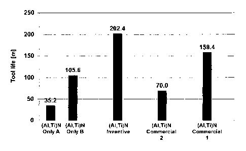
Furthermore it was verified that (AI,Ti)N coatings containing only structures
corresponding to the coating portion A or the coating portion B doesn't
exhibit
improved high cutting performance. The results can be observed in figure 3.
Figures nomenclature:
Figure 1: Comparison of cutting performance by milling operations in cutting
test 1.
Test conditions in cutting test 1 were:
Material: 1.4571
Tool: carbide insert ADKT 1505
Cutting parameters: Vc=125m/min, fz=0.15mm, ap=4mm, ae=35mm
Operation: face milling/dry
Figure 2: Comparison of cutting performance by turning operations in cutting
test 2.
Test conditions in cutting test 2 were:
Material: 1.4571
Tool: CNMG432
Cutting parameters: Vc=180m/min, fz=0.25mm, ap=2mm
Operation: wet cutting/outside turning
Criteria: Vbmax > 205 pm
7
CA 02850270 2014-03-27
WO 2013/045039 PCT/EP2012/003896
Figure 3: Comparison of cutting performance by turning operations in cutting
test 3.
Test conditions in cutting test 3 were:
Material: 1.2344 45 HRC
Tool: end-mill 0 1 Omm
Cutting parameters: Vc=180m/min, fz=0.1mm, ap=10mm, ae=0.5mm
Operation: wet cutting/finishing
Criteria: Vbmax ?. 100 pm
In the context of the present invention the nomenclatures (Ti,AI)N coatings
and
(AI,Ti)N coatings have the same meaning and hence were used indistinctive.
Commonly used arc evaporators by coatings processes include a cathode but not
a
specific anode because the anode is constituted by the coating chamber walls.
For
this reason, more of the electrons generated at the cathode must go across the
plasma in order to attain the anode. For this reason, more electrons arrive at
the
plasma during the arc PVD coating process.
In the case of the present invention, as it is mentioned above, the arc
evaporator
used for the production of the (AI,Ti)N coatings had an special configuration,
where
the anode is placed in the surroundings of the cathode and the magnetic field
configuration helps also to deviate a major quantity of electrons from the
cathode to
the anode, avoiding that the electrons arrive at the plasma during the arc PVD
process. It makes possible that a lower quantity of electrons generated at the
cathode arrive at the plasma and consequently it is possible to maintain the
electron
temperature and ionization grade of the reactive gas in the plasma during the
8
CA 02850270 2014-03-27
WO 2013/045039 PCT/EP2012/003896
deposition of the (AI,Ti)N coatings as low as possible, as it was described in
one of
the preferred embodiments of the present invention mentioned above.
Due to the used arc evaporator with a configuration which allows the deviation
of the
electrons from the cathode to the anode arranged in the direct neighborhood of
the
cathode it was possible to generate the necessary process conditions for
forming a
coating having portions A and B according to the present invention by
adjusting coil
current and substrate bias voltage. Higher coil current values were associated
with a
higher deviation of the electrons from the cathode to the anode.
The applied substrate bias voltages sbvA and sbvB varied between -30 V and -
200 V,
with sbvA > sbvB.
According to the realized experiments, the cutting tools coated according to
the
present invention show particularly good cutting performance if for depositing
the
coating portion A of the (AI,Ti)N coating the applied substrate bias voltage
is not
lower than -150 V (sbvA not having a more negative value than -150 V), and for
depositing the coating portion A of the (AI,Ti)N coating the applied substrate
bias
voltage is not lower than -200 V (sbvB not having a more negative value than -
200 V).
In other words, very good cutting performance can be attained according to the
present invention if the the bias voltage applied at the substrate during the
deposition
of the coating portion A is in absolute value lower than it applied during the
deposition of the coating portion B.
9
CA 02850270 2014-03-27
WO 2013/045039 PCT/EP2012/003896
Particularly, targets made by powder metallurgy techniques can be used for the
coating deposition but also composed targets or alloyed targets made by other
techniques can be used.
If it is necessary to improve the cohesiveness of the coating, it could be
recommendable to adjust coating parameters such as coil current and/or bias
voltage
at the beginning of the deposition of the respective coating portions A and B
gradually (e.g. by using a ramp).
In most instances, particularly good cutting performances were exhibited by
cemented carbide cutting tools coated according to the present invention when
the
grain size of both coating portions A and B was lower than 30 nm.
Particularly, in
some cases, when the average grain size of the coating portion A was about 20
nm
or less and the average grain size of the coating portion B was about 10 nm or
less.
Likewise, particularly good cutting performances for some applications can be
attained by coated cutting tools according to the present invention if the AI-
content in
atomic percentage in the coating portion A, 1-xA, is approximately 4 ¨ 10 %
lower
than it in the coating portion B, 1-xB:
= if 0.04 5 ((1-xEl) - (1-xA))/(1-XA) 5 0.10,
= more particularly, if 0.04 5 ((1-x8) - (1-XA))/(1-XA) 5 0.06
Furthermore, coatings deposited according to the present invention whose
compressive stress in the coating portion A was at least 15 % lower than in
the
CA 02850270 2014-03-27
WO 2013/045039 PCT/EP2012/003896
portion B, preferably at least 20 % lower, provided particularly good cutting
performance.
A coating according to the present invention can be applied on every kind of
substrate.
Particularly, a coating according to the present invention can be used for
protecting
surfaces that will be exposed to tribological contact.
A coating according to the present invention can also improve several
tribological
properties of surfaces exposed to tribological contact, such as hardness, wear
resistant, oxidation resistance, etc. Particularly, a coating according to the
present
invention can be used for coating machine components and tools.
A coating according to the present invention can be particularly beneficial
for
improving cutting performance of cutting tools.
For example, the substrate of the coated cutting tools according to the
present
invention can comprise or can consists of steel and/or cemented carbide,
and/or
ceramic, and/or cubic boron nitride.
Overall coatings thickness of the (AI,Ti)N coatings deposited according to the
present
invention are preferably not smaller than 0.5 pm and not larger than 30 pm.
11