Note: Descriptions are shown in the official language in which they were submitted.
CA 02850605,2014-03-31
AKZENTA PANEELE + PROFILE GMBH
Our Reference: CD 40865 / UAM
DEVICE AND METHOD FOR IMPROVED DIRECT PRINTING OF
DECORATIVE PANELS
The present invention relates to a device for improved direct printing of
decorative
panels and a method for improved direct printing of decorative panels.
The term decorative panel in the sense of the invention means wall, ceiling or
floor
panels comprising a decor applied to a carrier plate. Decorative panels are
used in
various ways in the field of interior construction of rooms as well as for the
decorative
cladding of structures, for example in exhibition stand constructions. One of
the most
common areas of application of decorative panels is their usage as a floor
paving.
Herein, the decorative panels often have a decor which should simulate a
natural
material.
Examples of such simulated natural materials are wood species such as maple,
oak,
birch, cherry wood, ash, walnut, chestnut, wenge or exotic wood such as Panga-
Panga, mahogany, bamboo and Bubinga. Moreover, natural materials, such as
stone
surfaces or ceramic surfaces, are often simulated.
Hitherto such decorative panels are often manufactured as laminates in which a
de-
corative paper preprinted with a desired decor is applied on a carrier plate
and a so-
called overlay, in turn, is applied onto the decorative layer. After a
counteracting pa-
per has been applied on the side of the carrier plate opposing the decorative
paper, if
desired, the layered structure obtained is firmly bonded together by means of
appro-
priate pressure and/or heat-activated adhesives.
Dependent on the desired areas of application of the decorative panels they
could be
produced from different materials. Herein, in particular the material of the
carrier can
be selected in dependence of the area of application. Thus, the carrier, for
example,
CA 02850605 2014-03-31
4 t
,
- 2 -
can consist of a wood-based material, inasmuch as the decorative panel is not
ex-
posed to excessive moisture or weather conditions. If the panel, for example,
is to be
used in wet rooms or in the outdoor area, the carrier, for example, can
consist of a
plastic material.
Herein, wood-based materials in the sense of the invention in addition to
solid wood-
based materials comprise materials such as plywood board, composite lumber,
blockboard, veneer plywood, laminated veneer lumber, parallel strand lumber
and
bending plywood. In addition wood-based materials in the sense of the
invention are
understood to include chipboards such as pressboards, extruded boards,
oriented
..
structural boards (OSB) and laminated strand lumber as well as wood fibre
materials
such as wood fibre insulation boards (HFD), hard and medium-hard fibreboards
(MB,
-
HFH) and particularly medium-density fibreboards (MDF) and high-density fibre-
boards (HDF). Moreover, modern wood-based materials such as wood-polymer ma-
terials (wood plastic composite, WPC), sandwich boards made of a lightweight
core
material such as foam, hard foam or paper honeycombs and a wood layer applied
thereon as well as chipboards minerally hardened, for example with cement, are
wood-based materials in the sense of the invention. Moreover, cork represents
a
wood-based material in the sense of the invention.
Plastic materials which can be used in the production of corresponding panels
are,
for example, thermoplastics such as polyvinyl chloride, polyolefines (such as
polyeth-
ylene (PE), polypropylene (PP)), polyamides (PA), polyurethanes (PU),
polystyrene
(PS), acrylonitril butadiene styrene (ABS), polymethyl methacrylate (PMMA),
poly-
carbonate (PC), polyethylene terephthalate (PET), polyether ether ketone
(PEEK) or
mixtures or copolymerizates thereof. The plastic materials can include common
fill-
ers, such as calcium carbonate (chalk), aluminum oxide, silicagel, quartz
powder,
wood flour, gypsum. In addition they can be coloured in a known way.
CA 02850605 2014-03-31
-3 -
In the sense of the invention the term "direct printing" means applying a
decor directly
onto the carrier of a panel or onto an unprinted fibre material layer applied
to the car-
rier. In contrast to conventional methods in which a decorative layer
previously print-
ed with a desired decor is applied onto the carrier in direct printing the
decor is print-
ed directly in the course of the panel production. Herein, different printing
techniques
can be used such as flexographic printing, offset printing or silk-screen
printing.
Herein, in particular digital printing techniques can be used such as inkjet
methods
and laser printing methods.
In the sense of the invention the term fibre materials means materials such as
paper
and non-woven fabrics on the basis of plant, animal, mineral or even synthetic
fibres
as well as cardboards. Examples of fibre materials on the basis of plant
fibres in ad-
dition to papers and non-woven fabrics made of cellulose fibres are biomass
such as
straw, maize straw, bamboo, leaves, algae extracts, hemp, cotton or oil palm
fibres.
Examples of animal fibres are keratin-based materials such as wool or
horsehair.
Examples of mineral fibre materials are mineral wool or glass wool.
For protecting the applied decorative layer normally a wearing or top layer is
applied
on top of the decorative layer. A wearing and/or top layer in the sense of the
inven-
tion is a layer applied as an outer finish which particularly protects the
decorative lay-
er against wear or damage by dirt, influence of moisture or mechanical impacts
such
as abrasion. Herein it can be provided that the wearing layer includes hard
materials
such as titan nitride, titan carbide, silicon nitride, silicon carbide, boron
carbide, tung-
sten carbide, tantalum carbide, aluminum oxide (corundum), zircon oxide or
mixtures
thereof, in order to increase the wear resistance. Herein, it can be provided
that the
hard material is included in an amount between 5% by weight and 40% by weight,
preferably between 15% by weight and 25% by weight, in the composition of the
CA 02850605 2014-03-31
- 4 -
wearing layer. The hard material preferably has an average core diameter
between
pm and 250 pm, more preferably between 10 pm and 100 pm. In this way it is
achieved in a preferred way that the composition of the wearing layer forms a
stable
dispersion and a decomposition or precipitation of the hard material within
the com-
5 position of the wearing layer can be avoided. For the formation of a
corresponding
wearing layer according to one embodiment of the invention it is provided that
the
composition including hard material and adapted to be cured by radiation is
applied
with a concentration between 10 g/m2 and 250 g/m2, preferably between 25 g/m2
and
100 g/m2. The application can be implemented, for example, by rollers, such as
rub-
10 ber rollers, or by means of pouring devices. According to a further
embodiment of the
invention it can be provided that the hard material at the time of application
of the
composition of the wearing layer is not included within the composition, but
is spread
in the form of particles onto the applied composition of the wearing layer and
subse-
quently is cured.
In many cases it is provided that a surface texture matching with the decor is
in-
cluded in such wearing or top layers. A surface texture matching with the
decor
means that the surface of the decorative panel comprises a haptic structure
which
according to its shape and pattern corresponds to the applied decor such as to
achieve a reproduction of a natural material as close to the original as
possible even
with respect to the haptic. Herein, it can be provided that the carrier plate
already
comprises a texture and an alignment of a printing tool for applying the decor
with
respect to the carrier plate is implemented by means of the texture of the
carrier plate
which is detected by optical methods. Herein, for aligning the printing tool
and the
carrier plate relative to each other a relative movement between the printing
tool and
the carrier plate necessary for the alignment is implemented by shifting the
carrier
plate or by shifting the printing tool. According to a further embodiment of
the inven-
tion it is provided that a texturing of the decorative panel is implemented
subse-
CA 02850605 2015-06-15
30324-13
- 5 -
quently to the application of the top and/or wearing layer. To this end it can
be pre-
ferred to apply as the top and/or wearing layer a curable composition and a
curing
process is done only to an extent that only a partial curing of the top and/or
wearing
layer is achieved. In the thus partially cured layer by means of appropriate
tools, such
as a hard metal texture roller or a die, a desired surface texture is
embossed. Herein,
the embossing process is implemented corresponding to the applied decor. In
order
to ensure a sufficient matching of the texture to be produced with the decor
it may be
provided that the carrier plate and the embossing tool are to be aligned to
each other
by corresponding relative movements. Subsequently to the production of the
desired
texture within the partially cured top and/or wearing layer a further curing
step is im-
plemented with respect to the now textured top and/or wearing layer.
One problem that may occur during direct printing of decorative panels is that
a dete-
rioration of the print image occurs in the course of the production process.
Depend-
ent on the selected printing method a visible blurring of the print image can
occur
during the production process. lf, for example, an inkjet method is used for
applying
the decor, after a certain production time period a clearly recognizable
blurring oc-
curs in the decor print image which is not attributable to possible
contaminations of
the printhead or a change of the ink.
Considering that, it is an object of the present invention to provide a device
and a
method which are able to overcome the problem known in the prior art.
CA 02850605 2015-06-15
30324-13
- 6 -
Thus, according to the invention a panel printing device is suggested which
com-
prises a supply means for a carrier to be printed and a printing mechanism,
wherein the panel printing device comprises at least one means for discharging
electrostatic charges from the carrier and at least one means for supplying
electro-
static charges onto the carrier disposed downstream of the means for
discharging
electrostatic charges.
Surprisingly it has been found that the provision of a means for discharging
electro-
static charges from the carrier to be printed in combination with at least one
means
for supplying electrostatic charges onto the carrier disposed downstream of
the
means for discharging electrostatic charges is adapted to avoid the occurrence
of
blurrings in the course of the production process. The undefined electrostatic
charge
within the carrier to be printed, which builds up in the course of the
production proc-
ess, results in an undefined deflection of the colour or ink drops on their
way from the
printhead to the surface to be printed. Herein, it is assumed that the
electrostatic field
which builds up on the carrier deflects the normally positively charged ink
particles in
an unpredictable way such that they will not impinge on the intended point on
the
surface to be printed. The thus induced inaccuracy of the application of
colour results
in a visible blurring of the print image. Dependent on the production speed
and the
selected carrier material this effect occurs in different manifestations such
that it is
assumed that carriers are charged electrostatically in dependence of the
carrier ma-
terial due to their transport within the production plant and this charging is
sufficient
to induce the observed effect.
Because a means for supplying electrostatic charges onto the carrier is
provided by
adjusting a defined electrostatic charge of the carrier and particularly of
the carrier
surface, respectively, the undefined deflection of ink drops due to an
unpredictable
electrostatic charging can be avoided. Herein, it surprisingly has been found
that the
CA 02850605,2014-03-31
=
- 7 -
print image compared to the sole discharge of electrostatic charges can
further be
improved.
Because the means for supplying electrostatic charges onto the carrier is
disposed
downstream, i.e. in the moving direction of the carrier behind, a means for
dischar-
ging electrostatic charges from the carrier and particularly spaced thereto,
herein a
particular precise electrostatic charge can be applied into and onto the
carrier, re-
spectively. Because at first the electrostatic charges are completely removed
the car-
rier can have a particular uniform and defined electrostatic charge and
charging, re-
spectively, during the print process, because local peak charges can be
prevented
from occuring. Herein, the way, i.e. positive or negative polarity, and the
quantity of
the introduced or applied charge can be selected depending on the carrier
material
and/or the printing method and/or other factors.
For example, the means for supplying electrostatic charges onto the carrier,
such as
a charging system, can comprise a charge generator for positive (+) or
negative (-)
polarity and as well be connected to a mains adapter or power supply in order
to ap-
ply charges onto the carrier or the carrier surface.
Thus, by providing a means for discharging electrostatic charges from the
carrier to
be printed in combination with at least one means for supplying electrostatic
charges
onto the carrier disposed downstream of the means for discharging
electrostatic
charges from the carrier the print image in direct printing onto the carrier
can be im-
proved significantly.
According to an embodiment of the invention it is provided that the means for
dis-
charging electrostatic charges from the carrier and/or the means for supplying
elec-
trostatic charges onto the carrier is configured as a bar comprising a surface
which
CA 02850605 2014-03-31
- 8 -
extends essentially parallel to a surface of the carrier and is directed
towards the di-
rection of the carrier. In particular, this surface of the bar serving as an
active charg-
ing and discharging surface, respectively, can extend over the entire width of
the car-
rier, i.e. essentially in an orientation perpendicular to the moving direction
of the car-
rier over the entire dimension of the carrier. Herein, a surface of the bar
extending
essentially parallel to the surface of the carrier can particularly mean, that
the bar at
least within the region which is electrostatically discharging or charging
substantially
has a uniform distance, such as with a deviation of 20%, particularly 10%,
e.g.
1%, from the carrier.
Such a bar can particularly be a member which is configured approximately
rectan-
gular and comprises two levelled aligned surfaces which are disposed in the
direction
of the carrier and in the opposite direction. For example, the means for
discharging
electrostatic charges from the carrier and/or the means for supplying
electrostatic
charges onto the carrier can be configured as a plane grinded bar. In
particular with
this configuration corona discharges can be avoided and peak charges or
changes of
charge can be prevented effectively such that a discharge and particularly an
elec-
trostatic charging with production of a highly uniform charge distribution can
be real-
ised particularly uniform and defined such that the print image, too, can be
particu-
larly defined and of high quality. Herein, an electrostatic charging can be
realised by
applying a defined voltage to the bar, wherein the type and the magnitude of
the
electrostatic charging can be influenced or adjusted by the type and the
magnitude of
the voltage. Herein, by electrically contacting the bar with the moving
carrier the elec-
trostatic charging can be improved. The same applies to an electrostatic
discharging,
wherein in this case, too, the discharging can be implemented by applying a
voltage
or by connecting to an electrical ground potential.
CA 02850605.2014-03-31
- 9 -
According to an embodiment of the invention it is provided that the means for
dis-
charging electrostatic charges at least comprises a roll, a brush or a lip
made of a
conductive material which electrically contacts the carrier at least in the
region of the
printing mechanism and which is connected to an electrical ground potential.
The
electrical ground potential, for example, can be provided by earthing.
In one embodiment of the invention it is provided that the discharge of the
electrical
charge is realised through a roll which is part of the supply means of the
printing
mechanism. In this way a compact structure of the device can be achieved.
Accord-
ing to a particular preferred embodiment of the invention it can be provided
that a
plurality of the means used for the transport of the carrier within the
production line
for producing decorative panels are configured such that possibly occuring
electro-
static charges can be discharged over these means.
The bar, the roll, the brush or the lip at least in the region of contact with
the carrier
are formed of a material comprising a conductivity of '1.103 Sm-1. Herein, in
particu-
lar it can be provided that the electrical resistance between the carrier and
the
ground potential is 0,5 f2, preferably 0,05 Q.
The bar, the roll, the brush or the lip by means of which the carrier is
contacted can,
for example in the contact region with the carrier, be made of an electrically
conduc-
tive metal such as steel, chrome, copper, aluminum, silver, or a conductive
alloy such
as brass or bronze. According to a further embodiment of the invention the
roll, the
brush or the lip at least partially consists of a conductive plastic material.
Examples of
appropriate electrically conductive plastic materials are poly-3,4-ethylene
dioxythio-
phene, doped polythiophene, doped polyethine, polyaniline and polypyrrol. An
advan-
tage of such conductive plastic materials over metals is that plastic
materials are
softer than metals such that a possible damage of the carrier by scratching
can be
CA 02850605 2015-06-15
30324-13
- 10 -
avoided. Alternatively it can be provided that the roll, the brush or the lip
at least at
the contact points with the carrier consists of a conductive tissue. This, for
example,
can be a synthetic tissue into which metal threads are woven.
According to a further embodiment of the invention it can be provided that it
com-
prises an ionizing means disposed upstream of the printing mechanism, by means
of
which an ionized airflow is guided over the carrier to be printed. It has been
found
that biasing with ionized air is adapted to decrease or increase the
electrostatic
charging of the carrier.
According to a particularly preferred embodiment of the invention the printing
mecha-
nism comprises an inkjet printhead.
Regarding the method the object is achieved by methods for direct printing of
decora-
tive panels, including the process steps:
providing a carrier to be printed;
supplying the carrier to a printing mechanism; and
- printing a decor onto the carrier by means of the printing
mechanism;
the carrier is treated with means for changing the electrostatic
charging of the carrier, at least one of before the carrier is supplied to the
printing mechanism and
during the printing process within the printing mechanism, by initially
electrostatically
discharging the carrier and subsequently supplying a defined charge amount to
the
carrier.
Regarding the technical features and advantages of the method it is completely
re-
ferred to the description of the device and vice versa.
CA 02850605 2014-03-31
- 11 -
According to an embodiment of the invention a discharging process is conducted
within a range of 7 kV or more, particularly 10 kV or more, such as in a range
bet-
ween 7 kV or more and 15 kV or less. As an alternative or in addition an
electrostatic
charging process can be conducted independently from the kind of the charge
within
a range between more than 0 kV and 15 kV or less, such as 10 kV or less. It
surpris-
ingly has been found that in particular a discharging process by a
predetermined
charge amount and/or a charging process by a predetermined charge amount can
result in a particular good print image.
According to one embodiment of the method the means for decreasing the electro-
static charge include electrically contacting the carrier with the ground
potential.
Herein it can be provided that the contact of the carrier is implemented by
means of a
bar, a roll, a brush or a lip made of a material having an electrical
conductivity 1.103
Sm-1.
According to a further embodiment of the method according to the invention it
can be
provided that the carrier is biased with an ionized airflow before and/or
during the
transport to the printing mechanism. It has been found that biasing with an
ionized
airflow is adapted to significantly decrease or increase an electrostatic
charge within
the carriers.
Hereinafter the invention is explained with reference to a figure.
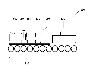
Figure 1 shows a panel printing device 100. The device 100 comprises a supply
means 110 fur supplying a carrier 600 to be printed by means of which the
carrier
600 is supplied to a printing mechanism 120. The printing mechanism 120
comprises
an inkjet printhead for applying a decor image onto the carrier under the
control of a
computer system. The device 100 comprises a means 130 for discharging electro-
CA 02850605,2014-03-31
,
,
- 12 -
static charges from the carrier 600 which may contact the carrier 600 and
further
comprises a means 170 for supplying electrostatic charges onto the carrier 600
which is disposed downstream of the means 130 for discharging electrostatic
charg-
es from the carrier 600 and may also contact the carrier 600. Herein, the
means 130
and the means 170 are disposed in the region of the supply means 110 and are
formed of a rectangular bar made of a conductive material, wherein the
discharging
means 130 is connected to a ground potential by means of an earthing 150 and
the
supply means 170 is connected to a mains adapter 180 or a power source.
CA 02850605,2014-0,3-31
,
- 13 -
List of reference symbols
100 Panel printing device
110 Supply means
120 Printing mechanism
130 Discharging means
150 Earthing
170 Charge supply means
180 Mains adapter
600 Carrier