Note: Descriptions are shown in the official language in which they were submitted.
CA 02852551 2014-05-16
GELATINOUS DIELECTRIC MATERIAL FOR HIGH VOLTAGE CONNECTOR
BACKGROUND OF THE INVENTION
The present invention relates to high voltage electrical connectors, such as
high voltage
circuit breakers, switchgear, and other electrical equipment. Typical
dielectric materials used
in high voltage applications include air, oil, or sulfur hexafluoride (SF6)
gas. Air requires a
long distance between contacts in order to reduce the likelihood of arcing in
high
voltage (e.g., 5+ kV) environments. Compared to air, oil requires shorter
distances between
contacts, but oil is subject to igniting when a fault occurs and may contain
harmful
polychlorinated biphenyls (PCBs). Like oil, SF6 gas requires relatively short
distances
between contacts, but use of SF6 gas is undesirable for environmental
protection reasons.
BRIEF DESCRIPTION OF THE DRAWINGS
Fig. 1 is a schematic cross-sectional diagram illustrating a connector
assembly in an open
position according to implementations described herein;
Fig. 2 is schematic cross-sectional diagram illustrating the connector
assembly of Fig. 1 in a
closed position;
Fig. 3 is a schematic cross-sectional diagram of a connector body of the
connector assembly
of Fig. 1; and
Fig. 4 is an enlarged schematic view of the pin assembly of the connector
assembly of Fig. 1.
DETAILED DESCRIPTION OF THE PREFERRED EMBODIMENTS
The following detailed description refers to the accompanying drawings. The
same reference
numbers in different drawings may identify the same or similar elements.
According to implementations described herein, a chamber filled with silicone
gel is used as
a dielectric material to isolate a contact pin assembly in a high voltage
electrical connector.
The silicone gel acts as a malleable insulating compound that is capable of
adhering,
separating, and re-adhereing to the contact pin assembly. The silicone gel
prevents voltage
- 1 -
CA 02852551 2014-05-16
from creeping along an insulated surface of the pin assembly and/or flashing
over or arcing
to conductive components of the high voltage electrical connector.
As used in this disclosure, the term "high voltage" refers to equipment
configured to operate
at a nominal system voltage above 5 kilovolts (kV). Thus, the term "high
voltage" refers to
equipment suitable for use in electric utility service, such as in systems
operating at nominal
voltages of about 5 kV to about 38 kV, commonly referred to as "distribution"
systems, as
well as equipment for use in "transmission" systems, operating at nominal
voltages above
about 38 kV. Applicable equipment may include a circuit breaker, a grounding
device,
switchgear, or other high voltage equipment.
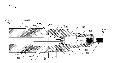
Fig. 1 is a schematic cross-sectional diagram illustrating a connector
assembly 10 in an open
position according to implementations described herein. Fig. 2 is a schematic
cross-sectional
diagram illustrating connector assembly 10 in a closed position. Connector
assembly 10 may
generally include a device body 100 and a pin assembly 200 that moves axially
within device
body 100 between the open position of Fig. 1 and the closed position of Fig.
2. Fig. 3 is a
schematic cross-sectional diagram of device body 100, and Fig. 4 is an
enlarged schematic
view of pin assembly 200.
Referring collectively to Figs. 1-4, device body 100 may include a connector
102 that is
connected to a bus 106. In one implementation, connector 102 may include a
threaded
connection, as shown. In other implementations, connector 102 may include a
spade
connector or another type of connector that is integrally formed with bus 106.
Connector 102
and bus 106 may be made of an electrically conductive material, such as
copper.
Connector 102 and/or bus 106 may extend through a bushing portion 104 of
device
body 100. Bushing portion 104 may form an insulative outer layer around bus
106 from
which connector 102 extends. Bushing portion 104 may be made of, for example,
an
insulative rubber or epoxy material. In one implementation, bushing portion
104 may be
sized as an ANSI standard high current interface.
As shown, for example, in Fig. 3, bus 106 may include an axial bore 108 formed
concentrically therein and a set of louver contacts 110. Bore 108 may be
configured to
receive pin assembly 200 such that pin assembly 200 may slide against louver
contacts 110,
- 2 -
CA 02852551 2014-05-16
as described further below. As shown in, for example, Fig. 3, bore 108 may
open into a larger
opening 109 of bushing portion 104.
Device body 100 may further include a conductive housing 112. Conductive
housing 112
may be made of an electrically conductive material, such as copper. Conductive
housing 112
may include a terminal connection or another interface (not shown) to other
electrical
equipment or to ground.
As shown in Fig. 3, conductive housing 112 may also include an axial center
bore 118
formed concentrically therein and a set of louver contacts 120. Although
implementations are
described herein using louver contacts 110/120, in other implementations a
different type of
contact may be used in bore 108 and bore 118. In other implementations, bore
108 and
bore 118 may simply include a contact region in place of louver contacts
110/120. Center
bore 118 may be configured to receive pin assembly 200 such that pin assembly
200 may
slide against louver contacts 120, as described further below. As shown in,
for example,
Fig. 3, center bore 118 may join a larger opening 119 of conductive housing
112.
As shown in Figs. 1 and 4, pin assembly 200 may include a non-conductive
(e.g., insulative)
tip 202 and a conductive pin 204. In one implementation, non-conductive tip
202 may be
formed from a plastic material, and conductive pin 204 may be formed from
copper. Non-
conductive tip 202 may include a threaded stud 206 and conductive pin 204 may
include a
corresponding threaded female opening 208 (or vice-versa) to secure non-
conductive tip 202
to conductive pin 204. In other embodiments, non-conductive tip 202 may be
chemically
bonded or adhered to conductive pin 204, such as with an epoxy or other
adhesive. Non-
conductive tip 210 may include a channel 210 configured to align with a
corresponding
channel 212 in conductive pin 204 to allow air to escape from bore 108 during
advancement
of pin assembly 200 into bore 108. Conductive pin 204 may also include a seat
214 for 0-
rings 216 to seal the interface between non-conductive tip 202 and conductive
pin 204.
Pin assembly 200 may move axially within bores 108/118 and openings 109/119.
Pin
assembly 200 may be driven, for example, by a motor (not shown) or other
mechanical force
between the open position shown in Fig. 1 and the closed position shown in
Fig. 2. In one
implementation, for example connector device 10 may be in communication with a
controller
- 3 -
CA 02852551 2014-05-16
that initiates a motor to selectively drive pin assembly 200 between the open
position of
Fig. 1 and the closed position of Fig. 2.
In one implementation, device body 100 and pin assembly 200 are configured to
provide
approximately two inches (e.g., an eighth inch) of axial distance ("D" in
Fig. 1) between
bus 106 and conductive pin 204 when connector assembly 10 is in an
open/ungrounded
position. Thus, the axial travel distance of pin assembly 200 may be between
about two and
three inches to ensure good contact between conductive pin 204 and louver
contacts 110
when connector assembly 10 is in a closed/grounded position.
Generally, in one implementation, pin assembly 200 may be configured so that
non-
conductive tip 202 is at least partially within bore 108 (e.g., in contact
with 0-rings 134,
described below) when connector assembly 10 is in the open position of Fig. 1
and is fully
within bore 108 (e.g., inserted past 0-rings 134) when connector assembly 10
is in the closed
position of Fig. 2. Also, conductive pin 204 may be at least partially within
bore 118 (e.g., in
contact with 0-rings 136, described below) when connector assembly 10 is in
the open
position of Fig. 1 or the closed position of Fig. 2. Thus, pin assembly 200
may always remain
anchored within bores 108 and 118 regardless of the particular open/closed
position of
connector device 10.
Opening 109 and opening 119 together may form a chamber 130 inside device body
100.
Consistent with aspects described herein, chamber 130 is be filled with a
solid or semi-solid
dielectric material. Particularly, in implementations described herein, a
silicone gel 132 may
serve as the dielectric insulating material. Several 0-rings 134, 136, and 138
may be used to
seal silicone gel 132 within chamber 130 and to provide a watertight
enclosure. More
particularly, 0-ring 134 may be seated along bore 108 adjacent pin assembly
200 near an
entrance to bore 108. Similarly, 0-ring 136 may be seated along bore 118
adjacent pin
assembly 200 near an entrance to bore 118. An additional 0-ring 138 may be
included at an
interface between bushing portion 104 and conductive housing 112. In one
implementation,
each of 0-rings 134, 136, and 138 may be made from identical elastomeric
materials to seal a
respective interface. In other implementations, one or more of 0-rings 134,
136, and 138 may
be made of different materials.
- 4 -
CA 02852551 2014-05-16
Silicone gel 132 may be inserted into chamber 130 via a port 140 (shown in
Fig. 3) after
bushing portion 104 and conductive housing 112 have been joined. Port 140 may
be
included, for example, through either bushing portion 104 or conductive
housing 112 (as
shown in Fig. 3). In an exemplary implementation, port 140 may include a
partially threaded
opening that can be plugged after insertion of silicone gel 132.
In one implementation, silicone gel 132 may be a transparent, two-part (e.g.,
including a base
and a crosslinker) silicone gel with a relatively low viscosity. In an
exemplary
implementation, silicone gel 132 may be cured within chamber 130 using, for
example, heat
or another accelerating process. In another implementation, silicone gel 132
may be cured
prior to insertion into chamber 130. Silicone gel 132 may also be self-
healing, in that silicone
gel 132 separates from a surface of pin assembly 200 when portions of pin
assembly 200
slide past 0-rings 134/136 and out of chamber 130. Silicone gel 132 may re-
adhere to the
surface of pin assembly 200 as portions of pin assembly 200 slide past 0-rings
134/136 and
back into chamber 130.
Silicone gel 132 in chamber 130 may be used as an insulation medium between
bus 106/louver contacts 110 and pin assembly 200 along non-conductive tip 202.
Silicone
gel 132 can hold off the voltage from arcing across a surface of non-
conductive tip 202 (e.g.,
over distance, D, shown in Fig. 1). Furthermore, silicone gel 132 allows
conductive pin 204
and non-conductive tip 202 to move in and out of bore 108 in order to
alternately make
contact with bus 106/louver contacts 110.
When conductive pin 204 is in contact with bus 106/louver contacts 110,
connector
assembly 10 may be in a closed condition, such that high voltage at conductive
housing 112
and voltage at connector 102 are the same (e.g., "X" Volts AC, as shown in
Fig. 2). When
non-conductive tip 202 is in contact with bus 106/louver contacts 110, non-
conductive
tip 202 and the silicone gel can separate conductive pin 204 from bus 106 to
eliminate arcing
to conductive pin 204 and/or conductive housing 112. Thus, when connector
assembly 10 is
open, high voltage at conductive housing 112 (e.g., "X" Volts AC, as shown in
Fig. 1) may
not be conducted to connector 102 (e.g., 0 Volts AC, as shown in Fig. 1). In
an exemplary
configuration for 25,000 Amp interfaces, use of silicone gel 132 as a
dielectric insulator
- 5 -
CA 02852551 2014-05-16
enables use of a relatively small distance, D (Fig. 1), between conductive pin
204 and
bus 106, when pin assembly 200 is in the open position. For example, distance
D may
generally be less than three inches and, more particularly, about two inches.
By contrast, the
distance required for using air as an insulating medium under similar
conditions would
exceed ten inches.
According to an implementation described herein, connector assembly 10 may be
assembled
by providing a bushing portion (e.g., bushing portion 104) including a
conductive bus having
a first bore, and providing a conductive housing (e.g., conductive housing
112) including a
second bore. A pin assembly (e.g., pin assembly 200) may be inserted into the
first bore and
the second bore. The pin assembly may include a conductive pin secured to a
non-conductive
tip, such that the pin assembly can move axially within the first and second
bores between a
closed position that provides an electrical connection between the conductive
bus and the
conductive housing and an open position that provides no electrical connection
between the
conductive bus and the conductive housing (e.g., that insulates the conductive
housing from
the conductive bus). The bushing portion and the conductive housing may be
joined to
axially align the first bore and the second bore and to form an internal
chamber (e.g., internal
chamber 130) around a portion of the pin assembly, such that the internal
chamber separates
the first bore and the second bore. A gelatinous silicone material (e.g.,
silicone gel 132) may
be inserted into the internal chamber via a port, to prevent or substantially
reduce the
likelihood of voltage arcing across a surface of the non-conductive tip when
the pin assembly
is in the open position.
In implementations described herein provide a high-voltage connector device
that includes a
device body and a pin assembly. The connector device may include a bushing
portion with a
conductive bus having a first bore, a conductive housing with a second bore
that is axially
aligned with the first bore, an internal chamber separating the first bore and
the second bore,
and a gelatinous silicone material enclosed within the internal chamber. The
pin assembly
may include a non-conductive tip and a conductive pin secured to the non-
conductive tip.
The pin assembly may be configured to move axially, within the first and
second bores,
between a closed position (e.g., that provides an electrical connection
between the conductive
bus and the conductive housing) and an open position (e.g., that provides no
electrical
- 6 -
CA 02852551 2015-12-09
connection between the conductive bus and the conductive housing). The
gelatinous silicone
material inhibits voltage arcing across a surface of the non-conductive tip
when the pin assembly
is in the open position.
The foregoing description of exemplary implementations provides illustration
and description,
but is not intended to be exhaustive or to limit the embodiments described
herein to the precise
form disclosed. Modifications and variations are possible in light of the
above teachings or may
be acquired from practice of the embodiments. For example, implementations
described herein
may also be used in conjunction with other devices, such as medium or low
voltage equipment.
No element, act, or instruction used in the description of the present
application should be
construed as critical or essential to the invention unless explicitly
described as such. Also, as
used herein, the article "a" is intended to include one or more items.
Further, the phrase "based
on" is intended to mean "based, at least in part, on" unless explicitly stated
otherwise.
- 7 -