Note: Descriptions are shown in the official language in which they were submitted.
CA 02852783 2014-04-17
WO 2013/063806
PCT/CN2011/081830
1
Power Stack Structure and Method
BACKGROUND
TECHNICAL FIELD
[0001] Embodiments of the subject matter disclosed herein generally
relate to
methods and systems and, more particularly, to the electrical and mechanical
structure of a power stack assembly.
DISCUSSION OF THE BACKGROUND
[0002] Press-pack semiconductor devices are in many applications powerful
components that are used for controlling a flow of electrical power or
converting
voltage, current or frequency necessary for connecting to a motor or a
generator, or
interfacing with a utility grid. The press-pack semiconductor devices are used
in
power conversion apparatuses (e.g., power converters) for a diverse range of
applications. Those applications include motor drives for oil and gas, metal,
water,
mining and marine industries, as well as power/frequency converters for
renewable
energy (wind, solar), and electric power industries. To utilize the full
potential of the
press-pack semiconductor devices, a proper mechanical design of the complete
assembly, including the press-pack semiconductor devices, heat sinks, bus bars
and
other components, is required.
[0003] The current and heat conducting interfaces of a press-pack
semiconductor device are designed to retain good conduction properties
throughout
the equipment lifetime. This is accomplished by creating a sufficient number
of
CA 02852783 2014-04-17
WO 2013/063806
PCT/CN2011/081830
2
stable metal-to-metal connections which can efficiently conduct current from
the
semiconductor device to the bus bar.
[0004] For power converters with press-pack power semiconductor devices,
the power semiconductor devices are stacked on top of each other under a
required
pressure to make electrical and thermal contacts to form an electrical circuit
and to
remove heat generated from losses during operation. The stack (power stack
assembly) may have single or plural of columns comprising power semiconductor
devices, heat sinks, insulators, bus bars and alike with a clamping mechanism
to
hold those components together. Pressure is applied to each column to assure
proper electrical and thermal contact between the individual press pack
modules.
The press-pack semiconductor devices are the core components in a power
converter or variable frequency drive for electric motors.
[0005] The power semiconductor devices may include Integrated Gate
Commutated Thyristor (IGCT), Insulated Gate Bipolar Transistor (IGBT),
Injection-
Enhanced Gate Transistor (IEGT), Thyristor (ETT or LTT), and diode modules.
For
high power medium voltage power converters, when used in applications such as
oil
and gas, electric power, steel mill, and offshore, the press-pack form is
preferred due
to its higher power density and higher power handling capability. Even more,
the
press-pack form is preferred for the ruggedness and benign failure condition
of the
press-pack semiconductor devices, i.e., due to strong mechanical clamping
force,
failure of press-pack components will not lead to an arc and plasma event,
unlike a
power semiconductor module in a plastic package.
[0006] An example of a power stack assembly 10 is shown in Figure 1A.
Figure 1A shows a clamping mechanism 12 and 14 that maintains under pressure
CA 02852783 2014-04-17
WO 2013/063806
PCT/CN2011/081830
3
plural press-pack power semiconductor devices 16, bus bars 18, and heat sinks
20.
The press-pack power semiconductor devices 16 are directly connected to the
bus
bars 18 while the heat sinks 20 directly contact the bus bars 18.
[0007] However, this arrangement increases the thermal impedance from the
press-pack power semiconductor device to the heat sink because a surface of
the
bus bar is not as flat (smooth) as the surface of the press-pack power
semiconductor
device. In this regard, it is noted that a face (pole face) of the heat sinks
20 and the
press-pack power semiconductor devices 16 are manufactured with a high degree
of
flatness while the commercially available bus bars 18 may include multiple
sheets of
copper laminated together. Thus, the flatness of the bus bar is typically
lower than
that of the heat sink or the press-pack power semiconductor device. This
flatness
difference between the press-pack power semiconductor device and the bus bar
determines an imperfect contact between these two elements, which degrades the
capability of the entire power stack assembly by increasing the thermal
resistance,
which is undesirable.
[0008] A different approach that overcomes some of the limitations
discussed
above proposes to mount a bus bar 22 on a side of a heat sink 20 as shown in
Figure 1B. However, this approach tends to increase a stray inductance in the
electrical circuit due to the increased distance between columns, which adds
more
electrical stress to the power switches and increase the power losses besides
adding
more parts and labor hours to the power stack assembling.
[0009] Accordingly, it would be desirable to provide systems and methods
that
avoid the afore-described problems and drawbacks.
CA 02852783 2014-04-17
WO 2013/063806
PCT/CN2011/081830
4
SUMMARY
[0010] According to one exemplary embodiment, there is a power conversion
apparatus that includes plural press-pack power semiconductor devices; plural
thermal and electric conducting blocks provided among the plural press-pack
power
semiconductor devices; and plural bus bars provided among the plural press-
pack
power semiconductor devices and the plural thermal and electric conducting
blocks
to form a first column that is clamped under a predetermined mechanical force.
The
plural bus bars are directly pressed in the one or more columns for electrical
connections, at least one press-pack power semiconductor device is sandwiched
between two thermal and electrical conducting blocks, and at least one bus bar
is
sandwiched between two thermal and electric conducting blocks.
[0011] According to another exemplary embodiment, there is a power
conversion apparatus that includes plural press-pack power semiconductor
devices;
plural thermal and electric conducting blocks provided among the plural press-
pack
power semiconductor devices; plural bus bars provided among the plural press-
pack
power semiconductor devices and the plural thermal and electric conducting
blocks
to form a first column that is clamped under a predetermined mechanical force;
first
and second insulators configured to sandwich the plural press-pack power
semiconductor devices, the thermal and electric conducting blocks, and the
plural
bus bars to form a first column so that ends of the first column are
electrically
insulated; and a stack frame configured to apply a predetermined rated force
to the
first and second insulators and the first column. The plural bus bars are
directly
pressed in the first column for electrical connections, at least one press-
pack power
semiconductor device is sandwiched between two thermal and electrical
conducting
CA 02852783 2014-04-17
WO 2013/063806 PCT/CN2011/081830
blocks, and at least one bus bar is sandwiched between two thermal and
electric
conducting blocks.
[0012] According to still another exemplary embodiment, there is a method
for
assembling a power conversion apparatus that provides optimum heat transfer
for
press-pack power semiconductor devices and minimum commutation loss and
stress.
The method includes a step of sandwiching press-pack power semiconductor
devices between corresponding thermal and electric conducting blocks to form a
first
column; a step of inserting bus bars into the first column so that at least
one bus bar
is provided between two thermal and electric conducting blocks; a step of
adding first
and second insulators to ends of the first column so that the ends of the
first column
are electrically insulated; and a step of applying a rated force on the first
column.
BRIEF DESCRIPTION OF THE DRAWINGS
[0013] The accompanying drawings, which are incorporated in and
constitute
a part of the specification, illustrate one or more embodiments and, together
with the
description, explain these embodiments. In the drawings:
[0014] Figures 1A-B are schematic diagrams of conventional power stack
assemblies;
[0015] Figure 2 is a schematic diagram of a power stack assembly
according
to an exemplary embodiment;
[0016] Figure 3 is a schematic diagram of another power stack assembly
according to an exemplary embodiment;
[0017] Figure 4 is a schematic diagram illustrating a flatness of a
surface
according to an exemplary embodiment;
CA 02852783 2014-04-17
WO 2013/063806
PCT/CN2011/081830
6
[0018] Figure 5 is a schematic diagram of a delta connected power stack
assembly according to an exemplary embodiment;
[0019] Figure 6 is a schematic diagram of a straight line connected power
stack assembly according to an exemplary embodiment; and
[0020] Figure 7 is a flow chart illustrating a method for assembling a
power
stack assembly in a power conversion apparatus according to an exemplary
embodiment.
DETAILED DESCRIPTION
[0021] The following description of the exemplary embodiments refers to
the
accompanying drawings. The same reference numbers in different drawings
identify
the same or similar elements. The following detailed description does not
limit the
invention. Instead, the scope of the invention is defined by the appended
claims. The
following embodiments are discussed, for simplicity, with regard to the
terminology and
structure of press-packed semiconductor devices stacked in a power stack
assembly of
a power conversion apparatus. However, the embodiments to be discussed next
are
not limited to these apparatuses.
[0022] Reference throughout the specification to "one embodiment" or "an
embodiment" means that a particular feature, structure, or characteristic
described in
connection with an embodiment is included in at least one embodiment of the
subject
matter disclosed. Thus, the appearance of the phrases "in one embodiment" or
"in an
embodiment" in various places throughout the specification is not necessarily
referring
to the same embodiment. Further, the particular features, structures or
characteristics
may be combined in any suitable manner in one or more embodiments.
CA 02852783 2014-04-17
WO 2013/063806
PCT/CN2011/081830
7
[0023] According to an exemplary embodiment, a power conversion apparatus
includes plural press-pack power semiconductor devices, plural heat sinks, and
at
least one bus bar that form at least a column. The bus bar is provided between
adjacent heat sinks so that a direct contact between the bus bar and the press-
pack
power semiconductor devices is avoided. In another exemplary embodiment, the
bus bar is distributed between a heat sink and a metal block so that direct
contact
between the bus bar and the press-pack power semiconductor devices is avoided.
The metal block may be in direct contact with the press-pack semiconductor
device.
A surface of the heat sink or of the metal block that directly faces the press-
pack
semiconductor devices may be manufactured to have a higher flatness than a
face
of the bus bar, thus reducing the thermal impedance. Also, for an arrangement
in
which more than one columns are formed, a thermal conduction path between the
press-pack semiconductor device and a corresponding heat sink is minimized and
electrical stresses are decreased due to the reduced commutation loop.
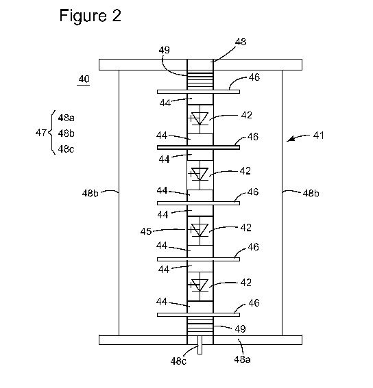
[0024] In an exemplary embodiment illustrated in Figure 2, a power stack
assembly 40 has one column that includes plural press-pack power semiconductor
devices 42. At least one press-pack power semiconductor device is sandwiched
between two heat sinks 44. In one application, each press-pack power
semiconductor device is sandwiched between two heat sinks 44. The press-pack
power semiconductor devices 42 may have a control gate 45. Bus bars 46 are
placed to be in direct contact with corresponding heat sinks 44 and not with
the
press-pack semiconductor devices 42. In one exemplary embodiment, no bus bar
46 is in direct contact with a press-pack power semiconductor device 42.
CA 02852783 2014-04-17
WO 2013/063806
PCT/CN2011/081830
8
[0025] An example of a press-pack power semiconductor device 42 is an
integrated gate-commutated thyristor (IGCT), an IGBT, or an IEGT. Another
example of a press-pack power semiconductor device is a diode
[0026] An IGCT or IEGT or press-pack IGBT device in a power stack
assembly needs to be pressed with a large force in order to function
efficiently from
an electrical and thermal point of view. One condition for achieving this
efficiency is
a uniform distributed force on a face (pole face) of the press-pack power
semiconductor device that faces and contacts the heat sinks 44. A smooth and
flat
pole face ensures uniform force distribution, good electrical contact and good
thermal transfer. Accordingly, the heat sinks need to have adequate mechanical
robustness to withstand compression with high forces without deformation,
e.g., up
to 135kN. Deformation could lead to inhomogeneous force distribution. Cast or
extruded heat sinks may be used. The heat sinks may also be made of Al or Cu.
Other materials may be used. The heat sinks may be machined properly through
processes such as milling or fine turning to get to the recommended surface
finish.
[0027] Not the same may be achieved for the bus bars 46. As the bus bars
46
are commercially available, these bus bars are made of sheets of copper or
other
material pressed together. However, such a process cannot achieve a flatness
comparable to that of the press-pack power semiconductor devices or the heat
sinks.
For this reason, according to this exemplary embodiment, the press-pack power
semiconductor devices 42 are sandwiched between the heat sinks 44 instead of
the
bus bars 46. Thus, the heat sinks decouple the negative effect induced by the
bus
bar when inserted in the column of the press-packed semiconductor devices.
CA 02852783 2014-04-17
WO 2013/063806
PCT/CN2011/081830
9
[0028] A stack frame 47 that includes first and second end plates 48a may
be
used to clamp together the press-pack power semiconductor devices, heat sinks
and
bus bars. The stack frame may be any of those known in the art. For example,
the
stack frame 47 may include rods 48b for maintaining the elements of the column
compressed with a desired force that is recommended for a good operation of
the
press-pack power semiconductor devices. A force application mechanism 48c may
be used to apply the desired force. Insulators 49 may be provided to sandwich
the
entire column of the power stack assembly 40 for preventing unwanted
electrical
contacts. The stack frame is configured to directly act on the insulators 49.
[0029] According to another exemplary embodiment illustrated in Figure 3,
a
column in a power stack assembly 50 may include press-pack power semiconductor
devices 52 that are sandwiched by heat sinks 54 or by a heat sink 54 and a
metal
block 56. In this exemplary embodiment, at least one bus bar 58 is not in
direct
contact with the press-pack power semiconductor devices. However, in another
exemplary embodiment, each bus bar is not in direct contact with the press-
pack
power semiconductor devices. A metal block 56 is preferred to the bus bar 58
as a
face of the metal block 56 facing the press-pack power semiconductor device
may
be manufactured to have a flatness comparable with that of the press-pack
power
semiconductor device. Although these metal blocks introduce a larger thermal
impedance compared with the heat sinks, they are a low cost alternative to
heat
sinks if they provide adequate thermal performance.
[0030] Figure 3 shows that the entire column of press-pack power
semiconductor devices, heat sinks and bus bars is sandwiched by insulating
elements 60 and clamped by a clamping mechanism that includes first and second
CA 02852783 2014-04-17
WO 2013/063806
PCT/CN2011/081830
ends 62 and 64. Each press-pack power semiconductor device 52 may be
electrically controlled via a corresponding gate 64.
[0031] In one exemplary embodiment, a flatness of the pole face of the
press-
pack power semiconductor devices and the heat sinks and/or metal blocks
directly
contacting the press-pack power semiconductor devices is 15 m or less. The
flatness is defined as shown in Figure 4. A specific pole face A is limited by
two
parallel planes B and C at a maximum distance of 15 m apart. To achieve this
flatness, the heat sink and the metal block may be made of a block of
aluminum,
copper or other metal while the bus bar, which has a poorer flatness, is made
of
laminated sheets of copper.
[0032] Figure 5 illustrates an embodiment in which a three-column IGCT
power stack assembly 80 has three columns 82, 84, and 86 connected in delta to
each other. A frame that maintains the columns in place and under a
predetermined
force is not shown as it is known in the art. For example, such a frame is
shown in
Figure 2. The power stack assembly 80 includes press-pack power semiconductor
devices (IGCT) 88 having a corresponding gate 90. The press-pack power
semiconductor device 88 is sandwiched by two heat sinks 92. However, the
columns may include diodes 94 as the press-pack power semiconductor devices
and
the diodes 94 are sandwiched between a heat sink 92 and a metal block 96. Bus
bars 100 are inserted in each column to directly contact the heat sinks 92 or
the
metal blocks 96 but not the press-pack power semiconductor devices 88.
[0033] In one exemplary embodiment, some bus bars may be inserted into
the
columns to directly contact the press-pack power semiconductor devices.
Insulators
102 may be used to electrically insulate each column from unwanted contacts at
its
CA 02852783 2014-04-17
WO 2013/063806
PCT/CN2011/081830
11
respective ends. As shown in Figure 5, a same bus bar 104 (collective bus bar)
may
extend to all three columns 82, 84, and 86. In other words, a single piece bus
bar
104 may electrically connect various elements in the three columns 82, 84, and
86.
The single piece bus bar 104 may have flexible parts 106 for ensuring that the
various parts that are inserted in the columns may slightly move one relative
to the
other. The flexible parts 106 may be formed between the columns 82, 84 and 86.
The single piece bus bar is made of a single piece of metal that forms a
closed loop
to minimize a commutation inductance.
[0034] Figure 6 shows another power stack assembly 200 having columns 82,
84 and 86 provided in-line. This embodiment shows that various insulators 102
may
be inserted into the columns. Figure 6 also shows that a heat sink 92a may
have
one inlet 110 and one outlet 112. A cooling piping system (not shown) may be
connected to the inlet 110 for pumping a cooling fluid inside the heat sink
92a and
after a heat transfer occurs between the fluid inside the heat sink 92a, the
hot
cooling fluid leaves the heat sink at outlet 112. In this way, the heat sink
92a is
cooled in a forced way to achieve a lower temperature of the press-packed
power
semiconductor device 88. While Figure 6 shows a heat sink configured to cool a
press-pack semiconductor device, it is noted that other elements of the power
stack
assembly, e.g., a resistor or inductor, may have a cooling channel built into
the
element.
[0035] The novel structures discussed above advantageously provides no
pole face of the press-packed semiconductor devices in contact with the bus
bars,
improves electrical and thermal performance, uses no screws for attaching the
bus
bars to the columns, reduces distances between columns, and reduces stray
CA 02852783 2014-04-17
WO 2013/063806 PCT/CN2011/081830
12
inductances. In addition, these novel structures require less labor hours for
assembly and disassembly.
[0036] According to an exemplary embodiment, there is a method for
assembling a power stack assembly that includes press-packed semiconductor
devices. The method includes a step 700 of sandwiching press-pack power
semiconductor devices (42) between corresponding thermal and electric
conducting
blocks (44) to form a first column; a step 702 of inserting bus bars (46) into
the first
column so that at least one bus bar is provided between two thermal and
electric
conducting blocks (44); a step 704 of adding first and second insulators (60)
to ends
of the first column so that the ends of the first column are electrically
insulated; and a
step 706 of applying a rated force on the first column.
[0037] The disclosed exemplary embodiments provide a system and a method
for a power stack assembly having press-packed power semiconductor devices to
improve electrical and thermal properties of the power stack assembly. It
should be
understood that this description is not intended to limit the invention. On
the contrary,
the exemplary embodiments are intended to cover alternatives, modifications
and
equivalents, which are included in the spirit and scope of the invention as
defined by
the appended claims. Further, in the detailed description of the exemplary
embodiments, numerous specific details are set forth in order to provide a
comprehensive understanding of the claimed invention. However, one skilled in
the
art would understand that various embodiments may be practiced without such
specific details.
[0038] Although the features and elements of the present exemplary
embodiments are described in the embodiments in particular combinations, each
CA 02852783 2014-04-17
WO 2013/063806
PCT/CN2011/081830
13
feature or element can be used alone without the other features and elements
of the
embodiments or in various combinations with or without other features and
elements
disclosed herein.
[0039] This written description uses examples of the subject matter
disclosed to
enable any person skilled in the art to practice the same, including making
and using
any devices or systems and performing any incorporated methods. The patentable
scope of the subject matter is defined by the claims, and may include other
examples
that occur to those skilled in the art. Such other examples are intended to be
within the
scope of the claims.