Note: Descriptions are shown in the official language in which they were submitted.
CA 02854161 2014-04-30
WO 2013/067181
PCT/US2012/063063
METHOD OF PREPARING THE SURFACE OF METAL SUBSTRATES FOR
ORGANIC PHOTOSENSITIVE DEVICES
Cross-Reference to Related Application
[0001] This application claims the benefit of U.S. Provisional Application No.
61/554,324, filed November 1, 2011, which is incorporated herein by reference
in its
entirety.
Statement Regarding Federally Sponsored Research
[0002] This invention was made with U.S. Government support under
Contract No. DE-SC0001013, awarded by the Department of Energy. The
government has certain rights in the invention.
Joint Research Agreement
[0003] The subject matter of the present disclosure was made by, on behalf
of, and/or in connection with one or more of the following parties to a joint
university-
corporation research agreement: University of Michigan and Global Photonic
Energy
Corporation. The agreement was in effect on and before the date the subject
matter
of the present disclosure was prepared, and was made as a result of activities
undertaken within the scope of the agreement.
[0004] The subject matter of the present disclosure is directed to a method
for preparing the surface of a metal substrate. The present disclosure also
relates to
an organic photovoltaic device comprising a metal substrate made by such
method.
Also disclosed herein is an inverted organic photosensitive optoelectronic
device
comprising a reflective electrode comprising stainless steel foil, an organic
donor-
acceptor heterojunction over the reflective electrode, and a transparent
electrode
over the donor-acceptor heterojunction.
1
CA 02854161 2014-04-30
WO 2013/067181
PCT/US2012/063063
[0005] Optoelectronic devices rely on the optical and electronic properties of
materials to either produce or detect electromagnetic radiation electronically
or to
generate electricity from ambient electromagnetic radiation.
[0006] Photosensitive optoelectronic devices convert electromagnetic
radiation into electricity. Solar cells, also called photovoltaic (PV)
devices, are a type
of photosensitive optoelectronic device that is specifically used to generate
electrical
power. PV devices, which may generate electrical energy from light sources
other
than sunlight, can be used to drive power consuming loads to provide, for
example,
lighting, heating, or to power electronic circuitry or devices such as
calculators,
radios, computers or remote monitoring or communications equipment. These
power generation applications also often involve the charging of batteries or
other
energy storage devices so that operation may continue when direct illumination
from
the sun or other light sources is not available, or to balance the power
output of the
PV device with a specific application's requirements. As used herein the term
"resistive load" refers to any power consuming or storing circuit, device,
equipment
or system.
[0007] Another type of photosensitive optoelectronic device is a
photoconductor cell. In this function, signal detection circuitry monitors the
resistance of the device to detect changes due to the absorption of light.
[0008] Another type of photosensitive optoelectronic device is a
photodetector. In operation, a photodetector is used in conjunction with a
current
detecting circuit which measures the current generated when the photodetector
is
exposed to electromagnetic radiation and may have an applied bias voltage. A
detecting circuit as described herein is capable of providing a bias voltage
to a
2
CA 02854161 2014-04-30
WO 2013/067181
PCT/US2012/063063
photodetector and measuring the electronic response of the photodetector to
electromagnetic radiation.
[0009] These three classes of photosensitive optoelectronic devices may be
characterized according to whether a rectifying junction as defined below is
present
and also according to whether the device is operated with an external applied
voltage, also known as a bias or bias voltage. A photoconductor cell does not
have
a rectifying junction and is normally operated with a bias. A PV device has at
least
one rectifying junction and is operated with no bias. A photodetector has at
least
one rectifying junction and is usually but not always operated with a bias. As
a
general rule, a photovoltaic cell provides power to a circuit, device or
equipment, but
does not provide a signal or current to control detection circuitry, or the
output of
information from the detection circuitry. In contrast, a photodetector or
photoconductor provides a signal or current to control detection circuitry, or
the
output of information from the detection circuitry but does not provide power
to the
circuitry, device or equipment.
[0010] Traditionally, photosensitive optoelectronic devices have been
constructed of a number of inorganic semiconductors, e.g., crystalline,
polycrystalline
and amorphous silicon, gallium arsenide, cadmium telluride and others. Herein
the
term "semiconductor" denotes materials which can conduct electricity when
charge
carriers are induced by thermal or electromagnetic excitation. The term
"photoconductive" generally relates to the process in which electromagnetic
radiant
energy is absorbed and thereby converted to excitation energy of electric
charge
carriers so that the carriers can conduct, i.e., transport, electric charge in
a material.
The terms "photoconductor" and "photoconductive material" are used herein to
refer
3
CA 02854161 2014-04-30
WO 2013/067181
PCT/US2012/063063
to semiconductor materials which are chosen for their property of absorbing
electromagnetic radiation to generate electric charge carriers.
[0011] PV devices may be characterized by the efficiency with which they
can convert incident solar power to useful electric power. Devices utilizing
crystalline
or amorphous silicon dominate commercial applications, and some have achieved
efficiencies of 23% or greater. However, efficient crystalline-based devices,
especially of large surface area, are difficult and expensive to produce due
to the
problems inherent in producing large crystals without significant efficiency-
degrading
defects. On the other hand, high efficiency amorphous silicon devices still
suffer
from problems with stability. Present commercially available amorphous silicon
cells
have stabilized efficiencies between 4 and 8%.
[0012] PV devices may be optimized for maximum electrical power
generation under standard illumination conditions (i.e., Standard Test
Conditions
which are 1000 W/m2, AM1.5 spectral illumination), for the maximum product of
photocurrent times photovoltage. The power conversion efficiency of such a
cell
under standard illumination conditions depends on the following three
parameters:
(1) the current under zero bias, i.e., the short-circuit current /sc, in
Amperes (2) the
photovoltage under open circuit conditions, i.e., the open circuit voltage
Vcc, in Volts
and (3) the fill factor, FF.
[0013] PV devices produce a photo-generated current when they are
connected across a load and are irradiated by light. When irradiated under
infinite
load, a PV device generates its maximum possible voltage, V open-circuit, or
Vcc.
When irradiated with its electrical contacts shorted, a PV device generates
its
maximum possible current, I short-circuit, or !sc. When actually used to
generate
power, a PV device is connected to a finite resistive load and the power
output is
4
CA 02854161 2014-04-30
WO 2013/067181
PCT/US2012/063063
given by the product of the current and voltage, I x V. The maximum total
power
generated by a PV device is inherently incapable of exceeding the product, 'so
x
Vcc. When the load value is optimized for maximum power extraction, the
current
and voltage have the values, !max and Vmax, respectively.
[0014] A figure of merit for PV devices is the fill factor, FF, defined as:
FF = { !max Vmax }/{ 'Sc VOC } (1)
where FF is always less than 1, as Isc and V00 are never obtained
simultaneously in
actual use. Nonetheless, as FF approaches 1, the device has less series or
internal
resistance and thus delivers a greater percentage of the product of Isc and
V00 to the
load under optimal conditions. Where Poic is the power incident on a device,
the
power efficiency of the device, tip, may be calculated by:
= FF* (Iso* V oc) I Pinc
[0015] To produce internally generated electric fields that occupy a
substantial volume of the semiconductor, the usual method is to juxtapose two
layers
of material with appropriately selected conductive properties, especially with
respect
to their distribution of molecular quantum energy states. The interface of
these two
materials is called a photovoltaic junction. In traditional semiconductor
theory,
materials for forming PV junctions have been denoted as generally being of
either n
or p type. Here n-type denotes that the majority carrier type is the electron.
This
could be viewed as the material having many electrons in relatively free
energy
states. The p-type denotes that the majority carrier type is the hole. Such
material
has many holes in relatively free energy states. The type of the background,
i.e., not
photo-generated, majority carrier concentration depends primarily on
unintentional
doping by defects or impurities. The type and concentration of impurities
determine
the value of the Fermi energy, or level, within the gap between the conduction
band
CA 02854161 2014-04-30
WO 2013/067181
PCT/US2012/063063
minimum and valance band maximum energies, also known as the HOMO-LUMO
gap. The Fermi energy characterizes the statistical occupation of molecular
quantum
energy states denoted by the value of energy for which the probability of
occupation
is equal to 1/2. A Fermi energy near the conduction band minimum (LUMO) energy
indicates that electrons are the predominant carrier. A Fermi energy near the
valence band maximum (HOMO) energy indicates that holes are the predominant
carrier. Accordingly, the Fermi energy is a primary characterizing property of
traditional semiconductors and the prototypical PV junction has traditionally
been the
p-n interface.
[0016] The term "rectifying" denotes, inter alia, that an interface has an
asymmetric conduction characteristic, i.e., the interface supports electronic
charge
transport preferably in one direction. Rectification is associated normally
with a built-
in electric field which occurs at the junction between appropriately selected
materials.
[0017] The current-voltage characteristics of organic heterojunctions are
often modeled using the generalized Shockley equation derived for inorganic
diodes.
However, since the Shockley equation does not rigorously apply to organic
semiconductor donor-acceptor (D-A) heterojunctions (HJs), the extracted
parameters
lack a clear physical meaning.
[0018] A significant property in organic semiconductors is carrier mobility.
Mobility measures the ease with which a charge carrier can move through a
conducting material in response to an electric field. In the context of
organic
photosensitive devices, a layer including a material that conducts
preferentially by
electrons due to a high electron mobility may be referred to as an electron
transport
layer, or ETL. A layer including a material that conducts preferentially by
holes due
6
CA 02854161 2014-04-30
WO 2013/067181
PCT/US2012/063063
to a high hole mobility may be referred to as a hole transport layer, or HTL.
In some
cases, an acceptor material may be an ETL and a donor material may be an HTL.
[0019] Conventional inorganic semiconductor PV cells may employ a p-n
junction to establish an internal field. However, it is now recognized that in
addition
to the establishment of a p-n type junction, the energy level offset of the
heterojunction may also play an important role. The energy level offset at the
organic donor-acceptor (D-A) heterojunction is believed to be important to the
operation of organic PV devices due to the fundamental nature of the
photogeneration process in organic materials. Upon optical excitation of an
organic
material, localized Frenkel or charge-transfer excitons are generated. For
electrical
detection or current generation to occur, the bound excitons must be
dissociated into
their constituent electrons and holes. Such a process can be induced by the
built-in
electric field, but the efficiency at the electric fields typically found in
organic devices
(F ¨ 106V/cm) is low. The most efficient exciton dissociation in organic
materials
occurs at a D-A interface. At such an interface, the donor material with a low
ionization potential forms a heterojunction with an acceptor material with a
high
electron affinity. Depending on the alignment of the energy levels of the
donor and
acceptor materials, the dissociation of the exciton can become energetically
favorable at such an interface, leading to a free electron polaron in the
acceptor
material and a free hole polaron in the donor material.
[0020] Organic PV cells have many potential advantages when compared to
traditional silicon-based devices. Organic PV cells are light weight,
economical in
materials use, and can be deposited on low cost substrates, such as flexible
plastic
foils. However, organic PV devices typically have relatively low quantum yield
(the
ratio of photons absorbed to carrier pairs generated, or electromagnetic
radiation to
7
CA 02854161 2014-04-30
WO 2013/067181
PCT/US2012/063063
electricity conversion efficiency), being on the order of 1 % or less. This
is, in part,
thought to be due to the second order nature of the intrinsic photoconductive
process. That is, carrier generation requires exciton generation, diffusion
and
ionization or collection. There is an efficiency q associated with each of
these
processes. Subscripts may be used as follows: P for power efficiency, EXT for
external quantum efficiency, A for photon absorption, ED for diffusion, CC for
collection, and INT for internal quantum efficiency. Using this notation:
r/P - r/ExT = r/A * r/ED * '/cc
r/ExT = r/A * r7/An-
[0021] The diffusion length (LD) of an exciton is typically much less (LD - 50
A) than the optical absorption length (-500 A), requiring a tradeoff between
using a
thick, and therefore resistive, cell with multiple or highly folded
interfaces, or a thin
cell with a low optical absorption efficiency.
[0022] Conventional organic PV cells are fabricated on transparent
substrates such as glass or plastic coated with a transparent conductor, such
as
indium tin oxide (ITO). Because these substrates can be expensive and/or an
important element of the overall cost structure of the device, the use of such
transparent conducting substrates has the potential to limit the cost-
effectiveness of
the overall device, especially in large-area applications. Inverted organic PV
cells
utilize a reflective substrate and a transparent top contact. This
architecture
eliminates the need for comparatively high-cost transparent substrates and
allows for
fabrication on arbitrary surfaces. This design significantly extends the
application of
organic PV cells, such as allowing for power-generating coatings or growth on
flexible and inexpensive opaque substrates. Accordingly, there exists a need
to
develop an efficient and low-cost method for preparing such substrates.
8
CA 02854161 2014-04-30
WO 2013/067181
PCT/US2012/063063
[0023] There is disclosed a method for preparing the surface of a metal
substrate, comprising:
(a) attaching a metal substrate to a rigid support structure to provide an
exposed top surface;
(b) mechanically polishing the exposed top surface of said metal substrate
with
an inorganic abrasive slurry for a time sufficient to reduce the surface
roughness of the
top surface; and
(c) applying an organic smoothing layer on the top surface to form a metal
substrate having a planarized top surface.
[0024] In one embodiment, the rigid support structure comprises a belt, disc
or plate, which can be made of any known rigid material, such as glass,
plastic, or
metal.
[0025] In one embodiment, the method described herein can be a continuous
process, or a batch process. When a continuous process is used, the rigid
support
structure should be suitably adapted, such as in the form of a belt.
[0026] In one embodiment, the metal substrate may be removed from the
rigid support structure prior to applying the organic layer. It is appreciated
that the
metal substrate can be bonded to the rigid support structure with any known
bonding
agents, such as a quartz wax. When a removable bonding agent is used, the
method may further comprise sonicating the metal substrate in at least one
solvent
to remove any residual quartz wax, such as xylene, prior to applying the
organic
smoothing layer.
[0027] In one embodiment, the organic smoothing layer can be applied via
solution processing, such as by one or more technique chosen from spin-
coating,
spin-casting, spray coating, dip coating, and doctor's blading.
9
CA 02854161 2014-04-30
WO 2013/067181
PCT/US2012/063063
[0028] In one embodiment, the organic smoothing layer comprises poly(3,4-
ethylene dioxythiophene):poly(styrene sulfonate) (PEDOT:PSS).
[0029] In one embodiment, the mechanical polishing is performed for a time
sufficient to reduce surface roughness below 20 nm, such as 3 nm or below. The
time sufficient to reduce surface roughness ranges from 15-60 minutes, such as
20-
50 minutes.
[0030] In one embodiment, the metal substrate comprises stainless steel,
which may be mechanically polished using a slurry such as an aqueous
suspension
comprising an abrasive material, including aluminum oxide, such as calcined
alumina.
[0031] The present disclosure also relates to organic photosensitive
optoelectronic devices, such as organic PV devices, grown in an inverted
manner.
For purposes of this disclosure, growth in an inverted manner means starting
with a
reflective electrode and using a transparent top electrode. In some
embodiments,
the inverted organic PV devices described herein comprise:
a reflective electrode;
an organic donor-acceptor heterojunction over the reflective electrode; and
a transparent electrode over the donor-acceptor heterojunction.
[0032] In some embodiments, the reflective electrode may comprise a
substrate, such as the metal substrate described herein. In some embodiments,
the
electrode may comprise a low work function metal selected from steel, Ni, Ag,
Al, Mg,
In, and mixtures or alloys thereof.
[0033] In certain embodiments, the inverted organic PV devices described
herein comprise: a surface-treated reflective electrode; an organic donor-
acceptor
CA 02854161 2014-04-30
WO 2013/067181
PCT/US2012/063063
heterojunction over the reflective electrode; and a transparent electrode over
the
donor-acceptor heterojunction.
[0034] In some embodiments, the donor of the organic donor-acceptor
heterojunction may be selected from phthalocyanines, porphyrins,
subphthalocyanines, and derivatives or transition metal complexes thereof. In
some
embodiments, the donor comprises boron subphthalocyanonine chloride (SubPc) or
copper phthalocyanine (CuPc). In some embodiments, the acceptor of the organic
donor-acceptor heterojunction is chosen from polymeric or non-polymeric
perylenes,
polymeric or non-polymeric naphthalenes, and polymeric or non-polymeric
fullerenes.
In some embodiments, the acceptor comprises C60 or 3,4,9,10-
perylenetetracarboxylic
bis-benzimidazole (PTCBI).
[0035] In some embodiments, the transparent electrode is chosen from
transparent oxides and metal or metal substitutes having a thickness
sufficient to
render them transparent or semi-transparent. In some embodiments, the
transparent
electrode is selected from transparent conducting oxides such as indium tin
oxide
(ITO), gallium
indium tin oxide (GITO), and zinc indium tin oxide (ZITO).
[0036] In some embodiments, the inverted organic PV devices described
herein may optionally comprise one or more blocking layers, such as an exciton
blocking layer (EBL), between the reflective electrode and the transparent
electrode.
In some embodiments, the EBL may be selected from molybdenum trioxide, N,N'-
diphenyl-N,N'-bis-alpha-naphthylbenzidine (NPD), aluminum tris (8-
hydroxyquinoline) (A1q3), carbazole biphenyl (CBP), bathocuproine (BCP), and
tris(acetylacetonato) ruthenium (III) (Ru(acac)3).
11
CA 02854161 2014-04-30
WO 2013/067181
PCT/US2012/063063
[0037] Also described herein are power-generating devices comprising at
least one organic PV device which comprises:
a reflective electrode;
an organic donor-acceptor heterojunction over the reflective electrode; and
a transparent electrode over the donor-acceptor heterojunction.
[0038] In some embodiments, the power-generating devices are formed on
the metal substrate described herein. In some embodiments, the power
generating
device is formed directly on the enclosure of a device, wherein the device
enclosure
functions as a substrate and the reflective electrode is formed over the
substrate.
[0039] A method for producing an organic PV device is also described,
comprising:
providing a reflective electrode;
performing at least one surface treatment on the reflective electrode;
forming an organic donor-acceptor heterojunction over the reflective
electrode; and
forming a transparent electrode over the organic donor-acceptor
heterojunction.
[0040] Also described are methods for generating and/or measuring
electricity. In some embodiments, the method comprises:
providing light to an organic PV device comprising a reflective electrode;
forming an organic donor-acceptor heterojunction over the reflective
electrode; and
forming a transparent electrode over the donor-acceptor heterojunction.
12
CA 02854161 2014-04-30
WO 2013/067181
PCT/US2012/063063
[0041] In some embodiments, the substrate is reflective, such as, for
example, a metal foil, and the electrode closest to the reflective substrate
is formed
from suitable transparent or semitransparent materials defined herein.
Brief Description of the Drawings
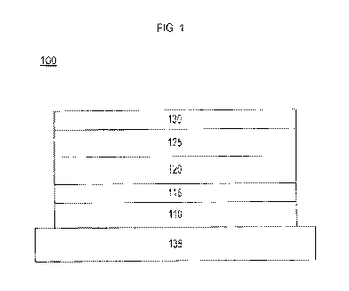
[0042] FIG. 1 shows an inverted organic PV device comprising a surface-
treated reflective electrode formed over a substrate, an organic donor-
acceptor
heterojunction on top of the reflective electrode, and a transparent electrode
on top
of the donor-acceptor heteroj unction.
[0043] FIG. 2 illustrates the surface of a stainless steel foil (SUS)
substrate
before and after polishing. FIG. 2(a) is a scanning electron microscope (SEM)
image
of the SUS substrate before polishing. FIG. 2(b) shows an SEM image of the SUS
substrate after polishing. FIG. 2(c) is an Atomic Force Microscopy (AFM) image
of
the same SUS substrate after polishing, exhibiting a reduced surface
roughness.
(Image area 5X5 pm, root-mean-square (RMS) roughness 1.63 nm.)
[0044] FIG. 3 illustrates surface roughness evolution of photosensitive
devices deposited on various substrates. Shown are the images and RMS surface
roughness of the layers, including substrate, Ag:Mg (first 50 A and 1200 A),
and C60,
during deposition successively on various substrates (from left to right,
glass, quartz,
thick 5i02 on Si, SUS, and Si) using AFM (image area 5X5 pm).
[0045] FIG. 4 illustrates surface roughness evolution of photosensitive
devices deposited on various substrates. Shown are the images and RMS surface
roughness of the layers, including SubPc, Mo03, and ITO, during deposition
successively on various substrates (from left to right, glass, thick 5i02 on
Si, SUS
and Si) using AFM (image area 5X5 pm).
13
CA 02854161 2014-04-30
WO 2013/067181
PCT/US2012/063063
[0046] FIG. 5 illustrates rip (square), Voc (circle), and FF (triangle) versus
power intensity for a planarlOPV (SUS/PEDOT:PSS/Ag:Mg/C60/SubPc/Mo03/1T0).
[0047] FIG. 6 illustrates the current density-voltage (J-V) characteristics
for
planar 10PV (SUS/PEDOT:PSS/Ag:Mg/C60/SubPc/Mo03/1TO) in the dark (square)
and under simulated one sun AM1.5G illumination (triangle).
[0048] FIG. 7 illustrates the current density-voltage (J-V) characteristics
for
planar 10PV (SUS/PEDOT:PSS/Ag:Mg/C60/SubPc/Mo03/1TO) in the dark (square)
and under simulated one sun AM1.5G illumination (triangle).
[0049] FIG. 8 illustrates the current density-voltage (J-V) characteristics
for
(1) conventional 10PV in the dark (square) and under one sun, AM1.5G simulated
illumination; (2)10PV on quartz substrate in the dark (circle) and under one
sun,
AM1.5G simulated illumination; (3)10PV on SUS substrate in the dark (triangle)
and
under one sun, AM1.5G simulated illumination. Fits according to the theory in
text
are indicated by the solid line, long dashed line and short dashed line for
devices (1),
(2) and (3), respectively.
[0050] Inverted organic photosensitive optoelectronic devices are described
herein. The organic devices described may be used, for example, to generate a
usable electrical current from incident electromagnetic radiation (e.g., PV
devices) or
may be used to detect incident electromagnetic radiation. Some embodiments may
comprise an anode, a cathode, and a photoactive region between the anode and
the
cathode. The photoactive region is the portion of the photosensitive device
that
absorbs electromagnetic radiation to generate excitons that may dissociate in
order
to generate an electrical current. The devices described herein may also
include at
least one transparent electrode to allow incident radiation to be absorbed
within the
14
CA 02854161 2014-04-30
WO 2013/067181
PCT/US2012/063063
device. Several PV device materials and configurations are described in U.S.
Patent
Nos. 6,657,378, 6,580,027, 6,352,777, and U.S. Patent Application Publication
No.
2010/0102304 which are incorporated herein by reference for their disclosure
of PV
device materials and configurations.
[0051] As used herein, the term "layer" refers to a member or component of
a photosensitive device whose primary dimension is X-Y, i.e., along its length
and
width. It should be understood that the term layer is not necessarily limited
to single
layers or sheets of materials. In addition, it should be understood that the
surfaces
of certain layers, including the interface(s) of such layers with other
material(s) or
layers(s), may be imperfect, wherein said surfaces represent an
interpenetrating,
entangled or convoluted network with other material(s) or layer(s). Similarly,
it
should also be understood that a layer may be discontinuous, such that the
continuity of said layer along the X-Y dimension may be disturbed or otherwise
interrupted by other layer(s) or material(s).
[0052] The terms "electrode" and "contact" are used herein to refer to a layer
that provides a medium for delivering photo-generated current to an external
circuit
or providing a bias current or voltage to the device. That is, an electrode,
or contact,
provides the interface between the active regions of an organic photosensitive
optoelectronic device and a wire, lead, trace or other means for transporting
the
charge carriers to or from the external circuit. Anodes and cathodes are
examples.
U.S. Patent No. 6,352,777, incorporated herein by reference for its disclosure
of
electrodes, provides examples of electrodes, or contacts, which may be used in
a
photosensitive optoelectronic device. In a photosensitive optoelectronic
device, it
may be desirable to allow the maximum amount of ambient electromagnetic
radiation
from the device exterior to be admitted to the photoconductively active
interior
CA 02854161 2014-04-30
WO 2013/067181
PCT/US2012/063063
region. That is, the electromagnetic radiation must reach a photoconductive
layer(s),
where it can be converted to electricity by photoconductive absorption. This
often
dictates that at least one of the electrical contacts should be minimally
absorbing and
minimally reflecting of the incident electromagnetic radiation. In some cases,
such a
contact should be substantially transparent. The opposing electrode may be a
reflective material so that light which has passed through the cell without
being
absorbed is reflected back through the cell. As used herein, a layer of
material or a
sequence of several layers of different materials is said to be "transparent"
when the
layer or layers permit at least about 50% of the ambient electromagnetic
radiation in
relevant wavelengths to be transmitted through the layer or layers. Similarly,
layers
which permit some, but less than about 50% transmission of ambient
electromagnetic radiation in relevant wavelengths are said to be "semi-
transparent."
[0053] The term "cathode" is used in the following manner. In a non-stacked
PV device or a single unit of a stacked PV device under ambient irradiation
and
connected with a resistive load and with no externally applied voltage, e.g.,
a PV
device, electrons move to the cathode from the photo-conducting material.
Similarly,
the term "anode" is used herein such that in a PV device under illumination,
holes
move to the anode from the photoconducting material, which is equivalent to
electrons moving in the opposite manner. It will be noted that as the terms
are used
herein, anodes and cathodes may be electrodes or charge transfer layers.
[0054] As used herein, "top" means furthest away from the substrate
structure (if present), while "bottom" means closest to the substrate
structure. If the
device does not include a substrate structure, then "top" means furthest away
from
the reflective electrode. For example, for a device having two electrodes, the
bottom
electrode is the electrode closest to the substrate structure, and is
generally the first
16
CA 02854161 2014-04-30
WO 2013/067181
PCT/US2012/063063
electrode fabricated. The bottom electrode has two surfaces, a bottom side
closest
to the substrate, and a top side further away from the substrate. Where a
first layer
is described as "disposed over" or "on top of" a second layer, the first layer
is
disposed further away from substrate. There may be other layers between the
first
and second layer, unless it is specified that the first layer is "in physical
contact with"
the second layer. For example, a cathode may be described as "disposed over"
or
"on top of" an anode, even though there are various organic layers in between.
[0055] FIG. 1 shows an example of inverted organic photosensitive
optoelectronic device 100. The figures are not necessarily drawn to scale.
Device
100 may include reflective substrate 110, donor layer 115, acceptor layer 120,
optional
blocking layer 125, and transparent electrode 130. Device 100 may be
fabricated by
depositing the layers described, in order. In some embodiments, the device
described
in FIG. 1 may optionally include a very thin, damage inducing metal layer
between
blocking layer 125 and transparent electrode 130 such that transparency is not
impacted. Device 100 may also optionally include substrate structure 135. In
some
embodiments, the substrate structure may directly support reflective electrode
110.
[0056] The specific arrangement of layers illustrated in FIG. 1 is exemplary
only, and is not intended to be limiting. For example, some of the layers
(such as
blocking layers) may be omitted. Other layers (such as reflective electrode or
additional acceptor and donor layers) may be added. The order of layers may be
altered. Arrangements other than those specifically described may be used.
Additionally, the organic PV device may exist as a tandem device comprising
one or
more additional donor-acceptor layers. A tandem device may have charge
transfer
layers, electrodes, or charge recombination layers between the tandem donor-
17
CA 02854161 2014-04-30
WO 2013/067181
PCT/US2012/063063
acceptor layers. The substrate and reflective electrode may be combined, the
substrate may be reflective and the electrode transparent.
[0057] In some embodiments, reflective electrode 110 and substrate material
135 may be combined or formed of two metals. In some embodiments substrate 135
is reflective and electrode 110 is transparent.
[0058] Substrate 135, onto which the device may be grown or placed, may
be any suitable material that provides the desired structural properties. The
substrate may be flexible or rigid, planar or non-planar. The substrate may be
transparent, translucent or opaque. Plastic, glass, and quartz are examples of
rigid
substrate materials. Plastic and metal foils are examples of flexible
substrate
materials. The material and thickness of the substrate may be chosen to obtain
the
desired structural and optical properties. In some embodiments, substrate 135
is
stainless steel, such as a stainless steel foil (SUS). SUS substrates are
relatively low
cost compared to conventional materials, and provide better heat sinks during
growth of layers.
[0059] In some embodiments, a metal substrate suitable to be used in
organic PV may be prepared by mechanical polishing to reduce surface
roughness,
for example, below 3 nm, or between 1-3 nm. In some other embodiments, the
surface of the metal substrate may be further smoothed by depositing a
smoothing
layer, such as an organic smoothing layer.
[0060] In some embodiments of the mechanical polishing process, a metal
substrate is attached to a rigid support structure to provide an exposed top
surface.
The rigid support structure may be a belt, disc or plate, which can be made of
any
known rigid material, such as glass, plastic, or metal. In one embodiment, the
method described herein can be a continuous process, or a batch process. When
a
18
CA 02854161 2014-04-30
WO 2013/067181
PCT/US2012/063063
continuous process is used, the rigid support structure should be suitably
adapted,
such as in the form of a belt.
[0061] In some embodiments, the metal substrate can be bonded to the rigid
support structure with any known bonding agents, such as a quartz wax.
[0062] The exposed top surface of the metal substrate may be mechanically
polished with inorganic abrasive slurry for a time sufficient to reduce the
surface
roughness of the surface. The slurry, such as an aqueous suspension, comprises
an abrasive material, for example, aluminum oxide, such as calcined alumina.
[0063] In one embodiment, the mechanical polishing is performed for a time
sufficient to reduce surface roughness to, for example, below 20 nm, such as
15 nm
or below, 12 nm or below, 10 nm or below, 5 nm or below, and 3 nm or below.
The
time sufficient to reduce surface roughness may range from 15-60 minutes, such
as
20-50 minutes, 20-40 minutes, 20-30 minutes, 15-45 minutes, and 30-45 minutes.
[0064] In one embodiment, the metal substrate may be removed from the
rigid support structure prior to applying the organic layer in the next step.
When a
removable bonding agent is used, the method may further comprise sonicating
the
metal substrate in at least one solvent to remove any residual quartz wax,
such as
xylene, prior to applying the organic smoothing layer.
[0065] In some embodiments, the obtained top surface may be further
planarized by applying an organic smoothing layer. In one embodiment, the
organic
smoothing layer comprises poly(3,4-ethylene dioxythiophene):poly(styrene
sulfonate) (PEDOT:PSS).
[0066] In one embodiment, the organic smoothing layer can be applied via
solution processing, such as by one or more techniques chosen from spin-
coating,
spin-casting, spray coating, dip coating, and doctor's blading.
19
CA 02854161 2014-04-30
WO 2013/067181
PCT/US2012/063063
[0067] In some other embodiments, the present disclosure also relates to
organic photosensitive optoelectronic devices, such as organic PV devices,
grown in
an inverted manner. For purposes of this disclosure, growth in an inverted
manner
means starting with a reflective electrode and using a transparent top
electrode. In
some embodiments, the inverted organic PV devices described herein comprise:
a reflective electrode;
an organic donor-acceptor heterojunction over the reflective electrode; and
a transparent electrode over the donor-acceptor heterojunction.
[0068] In some embodiments, the reflective electrode may comprise a
substrate, such as the metal substrate described herein. In some embodiments,
the
electrode may comprise a low work function metal selected from steel, Ni, Ag,
Al, Mg,
In, and mixtures or alloys thereof.
[0069] In certain embodiments, the inverted organic PV devices described
herein comprise: a surface-treated reflective electrode; an organic donor-
acceptor
heterojunction over the reflective electrode; and a transparent electrode over
the
donor-acceptor heterojunction.
[0070] Other than in the examples, or where otherwise indicated, all numbers
expressing quantities of ingredients, reaction conditions, analytical
measurements,
and so forth used in the specification and claims are to be understood as
being
modified in all instances by the term "about." Accordingly, unless indicated
to the
contrary, the numerical parameters set forth in the specification and attached
claims
are approximations that may vary depending upon the desired properties sought
to
be obtained by the present disclosure. At the very least, and not as an
attempt to
limit the application of the doctrine of equivalents to the scope of the
claims, each
CA 02854161 2014-04-30
WO 2013/067181
PCT/US2012/063063
numerical parameter should be construed in light of the number of significant
digits
and ordinary rounding approaches.
[0071] Notwithstanding that the numerical ranges and parameters setting
forth the broad scope of the disclosure are approximations, unless otherwise
indicated the numerical values set forth in the specific examples are reported
as
precisely as possible. Any numerical value, however, inherently contains
certain
errors necessarily resulting from the standard deviation found in their
respective
testing measurements.
[0072] In some embodiments, the "electrodes" described herein may be
composed of "metal" or "metal substitutes." Herein, the term "metal" is used
to
embrace both materials composed of an elementally pure metal, e.g., Mg, and
also
metal alloys which are materials composed of two or more elementally pure
metals,
e.g., Mg and Ag together, denoted Mg:Ag. Here, the term "metal substitute"
refers to
a material that is not a metal within the normal definition, but which has the
metal-like
properties that are desired in certain appropriate applications. Commonly used
metal substitutes for electrodes and charge transfer layers would include
doped
wide-bandgap semiconductors, for example, transparent conducting oxides such
as
indium tin oxide (ITO), gallium indium tin oxide (G ITO), and zinc indium tin
oxide
(ZITO). In particular, ITO is a highly doped degenerate n+ semiconductor with
an
optical bandgap of approximately 3.2 eV, rendering it transparent to
wavelengths
greater than approximately 3900 A. Another suitable metal substitute is the
transparent conductive polymer polyaniline (PAN I) and its chemical relatives.
[0073] Metal substitutes may be further selected from a wide range of non-
metallic materials, wherein the term "non-metallic" is meant to embrace a wide
range
of materials, provided that the material is free of metal in its chemically
uncombined
21
CA 02854161 2014-04-30
WO 2013/067181
PCT/US2012/063063
form. When a metal is present in its chemically uncombined form, either alone
or in
combination with one or more other metals as an alloy, the metal may
alternatively
be referred to as being present in its metallic form or as being a "free
metal". Thus,
the metal substitute electrodes described herein may sometimes be referred to
as
"metal-free," wherein the term "metal-free" is expressly meant to embrace a
material
free of metal in its chemically uncombined form. Free metals typically have a
form of
metallic bonding that results from a sea of valence electrons which are free
to move
in an electronic conduction band throughout the metal lattice. While metal
substitutes may contain metal constituents, they are "non-metallic" on several
bases.
They are neither pure free-metals nor are they alloys of free-metals. When
metals
are present in their metallic form, the electronic conduction band tends to
provide,
among other metallic properties, a high electrical conductivity as well as a
high
reflectivity for optical radiation.
[0074] Transparent electrode 130 may be chosen from transparent oxides
and metal or metal substitutes having a thickness sufficient to render them
transparent. Commonly used metal substitutes for electrodes and charge
transfer
layers would include doped wide-bandgap semiconductors, for example,
transparent
conducting oxides. In some embodiments, transparent electrode 130 may be
selected from ITO, G ITO, and ZITO. Other exemplary electrodes include highly
transparent, non-metallic, low resistance cathodes such as those disclosed in
U.S.
Patent No. 6,420,031, to Parthasarathy et al., or a highly efficient, low
resistance
metallic/non-metallic compound cathode such as those disclosed in U.S. Patent
No.
5,703,436 to Forrest et al., both incorporated herein by reference for their
disclosure
of cathodes. Each type of cathode is typically prepared in a fabrication
process that
includes the step of sputter depositing an ITO layer onto either an organic
material,
22
CA 02854161 2014-04-30
WO 2013/067181
PCT/US2012/063063
such as CuPc, to form a highly transparent, non-metallic, low resistance
cathode or
onto a thin Mg:Ag layer to form a highly efficient, low resistance
metallic/non-metallic
compound cathode.
[0075] The devices described herein will comprise at least one "photoactive
region" in which light is absorbed to form an excited state, or "exciton",
which may
subsequently dissociate in to an electron and a hole. The dissociation of the
exciton
will typically occur at the "heterojunction" formed by the juxtaposition of a
donor layer
and an acceptor layer. For example, in the device of FIG. 1, the "photoactive
region"
may include donor layer 115 and acceptor layer 120. Charge separation may
occur
predominantly at the organic heterojunction between donor layer 115 and
acceptor
layer 120. The built-in potential at the heterojunction is determined by the
HOMO-
LUMO energy level difference between the two materials contacting to form the
heterojunction. The HOMO-LUMO gap offset between the donor and acceptor
materials produces an electric field at the donor-acceptor interface that
facilitates
dissociation of excitons created within an exciton diffusion length of the
interface into
opposite signed carriers (holes and electrons).
[0076] Suitable materials comprising acceptor layer 120 may include, for
example, polymeric or non-polymeric perylenes, naphthalenes, fullerenes or
nanotubules. In some embodiments, acceptor layer 120 may comprise C60,
3,4,9,10-perylenetetracarboxylic bis-benzimidazole (PTCBI). In other
embodiments,
acceptor layer 120 may comprise a fullerene material as described in U.S.
Patent
No. 6,580,027, the description of fullerene material which is incorporated
herein by
reference. In some embodiments, donor layer 115 may comprise squaraines,
phthalocyanine, porphyrin, boron subphthalocyanonine chloride (SubPc), copper
23
CA 02854161 2014-04-30
WO 2013/067181
PCT/US2012/063063
phthalocyanine (CuPc), or a derivative or transition metal complex thereof
such as
aluminum phthalocyanine chloride (AICIPc).
[0077] Other suitable organic materials for use in the photoactive layers may
include cyclometallated organometallic compounds. The term "organometallic" as
used herein is as generally understood by one of ordinary skill in the art and
as
given, for example, in "Inorganic Chemistry" (2nd Edition) by Gary L. Miessler
and
Donald A. Tarr, Prentice Hall (1998). Thus, the term organometallic may refer
to
compounds which have an organic group bonded to a metal through a carbon-metal
bond. Organometallic compounds may comprise, in addition to one or more carbon-
metal bonds to an organic species, one or more donor bonds from a heteroatom.
The carbon-metal bond to an organic species may refer, for example, to a
direct
bond between a metal and a carbon atom of an organic group, such as phenyl,
alkyl,
alkenyl, etc. The term cyclometallated refers to compounds that comprise a
bidentate organometallic ligand so that, upon bonding to a metal, a ring
structure is
formed that includes the metal as one of the ring members.
[0078] As alluded to above with respect to the term "layer," it should be
understood that the boundary of acceptor layer 120 and donor layer 115, as
depicted
in FIG. 1, may be imperfect, discontinuous, and/or otherwise represent an
interpenetrating, entangled or convoluted network of donor and acceptor
materials.
For example, in some embodiments, while the organic donor-acceptor
heterojunction
may form a planar heterojunction, in others it may form a bulk heterojunction,
nanocrystalline bulk heterojunction, hybrid planar-mixed heterojunction, or
mixed
heterojunction. In some embodiments, two or more organic donor-acceptor
heterojunctions may be used to create a tandem inverted PV device.
24
CA 02854161 2014-04-30
WO 2013/067181
PCT/US2012/063063
[0079] Organic layers may be fabricated using vacuum deposition, spin
coating, organic vapor-phase deposition, inkjet printing, and other methods
known in
the art.
[0080] Organic photosensitive optoelectronic devices of the embodiments
described herein may function as a PV device, photodetector or photoconductor.
Whenever the organic photosensitive optoelectronic devices described herein
function as a PV device, the materials used in the photoconductive organic
layers
and the thicknesses thereof may be selected, for example, to optimize the
external
quantum efficiency of the device. Whenever the organic photosensitive
optoelectronic devices described herein function as photodetectors or
photoconductors, the materials used in the photoconductive organic layers and
the
thicknesses thereof may be selected, for example, to maximize the sensitivity
of the
device to desired spectral regions.
[0081] The device of FIG. 1 may further include one or more of blocking
layer 125, such as the exciton blocking layers (EBLs) described in U.S. Patent
No.
6,097,147 and U.S. Patent No. 6,451,415, Forrest et al., each of which is
incorporated herein by reference for their disclosure of blocking layers. In
certain
embodiments, higher internal and external quantum efficiencies have been
achieved
by the inclusion of an EBL to confine photogenerated excitons to the region
near the
dissociating interface and to prevent parasitic exciton quenching at a
photosensitive
organic/electrode interface. In addition to limiting the volume over which
excitons
may diffuse, an EBL can also act as a diffusion barrier to substances
introduced
during deposition of the electrodes. In some circumstances, an EBL can be made
thick enough to fill pinholes or shorting defects which could otherwise render
an
organic PV device non-functional. An EBL can therefore help protect fragile
organic
CA 02854161 2014-04-30
WO 2013/067181
PCT/US2012/063063
layers from damage produced when electrodes are deposited onto the organic
materials.
[0082] Without being bound to any particular theory, it is believed that the
EBLs derive their exciton blocking property from having a LUMO-HOMO energy gap
substantially larger than that of the adjacent organic semiconductor from
which
excitons are being blocked. Thus, the confined excitons are prohibited from
existing
in the EBL due to energy considerations. While it is desirable for the EBL to
block
excitons, it is not desirable for the EBL to block all charge. However, due to
the
nature of the adjacent energy levels, an EBL may block one sign of charge
carrier.
By design, an EBL will exist between two other layers, usually an organic
photosensitive semiconductor layer and an electrode, a charge transfer layer
or a
charge recombination layer. The adjacent electrode or charge transfer layer
will be
in context either a cathode or an anode. Therefore, the material for an EBL in
a
given position in a device will be chosen so that the desired sign of carrier
will not be
impeded in its transport to the electrode or charge transfer layer. Proper
energy
level alignment ensures that no barrier to charge transport exists, preventing
an
increase in series resistance. In certain embodiments, it may be desirable for
a
material used as a cathode side EBL to have a LUMO energy level closely
matching
the LUMO energy level of the adjacent acceptor material so that any undesired
barrier to electrons is minimized.
[0083] It should be appreciated that the exciton blocking nature of a material
is not necessarily an intrinsic property of its HOMO-LUMO energy gap. Whether
a
given material will act as an exciton blocker depends upon the relative HOMO
and
LUMO energy levels of the adjacent organic photosensitive material. Therefore,
it
may not be possible to identify a class of compounds in isolation as exciton
blockers
26
CA 02854161 2014-04-30
WO 2013/067181
PCT/US2012/063063
without regard to the device context in which they may be used. However, with
the
teachings herein, one of ordinary skill in the art may identify whether a
given material
will function as an exciton blocking layer when used with a selected set of
materials
to construct an organic PV device.
[0084] In some embodiments, blocking layer 125 may comprise an EBL
situated between acceptor layer 120 and transparent electrode 130. Examples of
suitable EBL materials include, but are not limited to, 2,9-dimethy1-4,7-
dipheny1-1,10-
phenanthroline (also called bathocuproin or BCP), which is believed to have a
LUMO-HOMO energy level separation of about 3.5 eV, or bis(2-methy1-8-
hydroxyquinolinoato)-aluminum(111)phenolate (Alq2OPH). BCP may be an effective
exciton blocker which can easily transport electrons to the cathode from an
acceptor
layer. In other embodiments, the EBL may be selected from molybdenum trioxide,
N,N'-diphenyl-N,N'-bis-alpha-naphthylbenzidine (NPD), aluminum tris (8-
hydroxyquinoline) (A1q3), carbazole biphenyl (CBP), and tris(acetylacetonato)
ruthenium (111) (Ru(acac)3).
[0085] In some embodiments, blocking layer 125 may comprise an EBL
doped with a suitable dopant, including but not limited to 3,4,9,10-
perylenetracarboxylic dianhydride (PTCDA), 3,4,9,10-perylenetracarboxylic
diimide
(PTCDI), 3,4,9,10-perylenetetracarboxylic-bis-benzimidazole (PTCBI), 1,4,5,8-
naphthalenetetracarboxylic dianhydride (NTCDA), and derivatives thereof. BCP,
as
deposited in the devices described herein, may be amorphous. Amorphous BCP
exciton blocking layers may exhibit film recrystallization, which may be
especially
rapid under high light intensities. The resulting morphology change to
polycrystalline
material results in a lower quality film with possible defects such as shorts,
voids or
intrusion of electrode material. Accordingly, it has been found that doping of
some
27
CA 02854161 2014-04-30
WO 2013/067181
PCT/US2012/063063
EBL materials, such as BCP, that exhibit this effect with a suitable,
relatively large
and stable molecule can stabilize the EBL structure to prevent performance
degrading morphology changes. It should be further appreciated that doping of
an
EBL which is transporting electrons in a given device with a material having a
LUMO
energy level close to that of the EBL may help to insure that electron traps
are not
formed which might produce space charge build-up and reduce performance.
Additionally, it should be appreciated that relatively low doping densities
should
minimize exciton generation at isolated dopant sites. Since such excitons are
effectively prohibited from diffusing by the surrounding EBL material, such
absorptions reduce device photoconversion efficiency.
[0086] In some embodiments, the device of FIG. 1 may further comprise one
or more transparent charge transfer layers or charge recombination layers. As
described herein, charge transfer layers are distinguished from acceptor and
donor
layers by the fact that charge transfer layers are frequently, but not
necessarily,
inorganic (often metals) and they may be chosen not to be photoconductively
active.
The term "charge transfer layer" is used herein to refer to layers similar to
but
different from electrodes in that a charge transfer layer only delivers charge
carriers
from one subsection of an optoelectronic device to the adjacent subsection.
The
term "charge recombination layer" is used herein to refer to layers similar to
but
different from electrodes in that a charge recombination layer allows for the
recombination of electrons and holes between tandem photosensitive devices and
may also enhance internal optical field strength near one or more active
layers. A
charge recombination layer can be constructed of semi-transparent metal
nanoclusters, nanoparticles or nanorods as described in U.S. Patent No.
6,657,378,
28
CA 02854161 2014-04-30
WO 2013/067181
PCT/US2012/063063
the disclosure of such semi-transparent metal nanoclusters, nanoparticles and
nanorods which is incorporated herein by reference.
[0087] In some other embodiments, a smoothing layer may be situated
between reflective electrode 110 (e.g., anode) and donor layer 115. A
exemplary
material for this layer comprises a film of 3,4-polyethylenedioxythiophene:
polystyrenesulfonate (PEDOT:PSS). The introduction of the PEDOT:PSS layer
between reflective electrode 110 (e.g., anode comprising ITO) and donor layer
115
(e.g., Cu Pc) may lead to greatly improved fabrication yields. Without being
bound to
a particular theory, it is believed that the improved fabrication yields may
be a result
of the ability of the spin-coated PEDOT:PSS film to planarize the ITO, whose
rough
surface could otherwise result in shorts through the thin molecular layers.
[0088] In a further embodiment, one or more of the layers of the FIG. 1
device may undergo surface treatments. For example, one or more of the layers
may be treated with plasma prior to depositing the next layer. The layers may
be
treated, for example, with a mild argon or oxygen plasma. This treatment may
be
beneficial in reducing the series resistance. It may be advantageous to
subject an
optional PEDOT:PSS layer to a mild plasma treatment prior to deposition of the
next
layer. Alternatively, one or more of the layers may be exposed to ultra-violet
ozone
(UV-03) treatment. In at least one embodiment, the reflective electrode (e.g.,
anode
layer) is exposed to a surface treatment.
[0089] The embodiments described herein also include a method for
producing the organic PV device of FIG. 1, comprising: providing reflective
electrode
110, performing at least one surface treatment on reflective electrode 110,
forming
an organic donor-acceptor heterojunction (e.g., donor layer 115 and acceptor
layer
29
CA 02854161 2014-04-30
WO 2013/067181
PCT/US2012/063063
120) over reflective electrode 110, and forming transparent electrode 130 over
said
organic donor-acceptor heterojunction.
[0090] The embodiments described herein also include methods for
generating and/or measuring electricity. In some embodiments, that method
comprises: providing light to the device of FIG. 1, which comprises reflective
electrode 110, organic donor-acceptor heterojunction on top of said reflective
electrode (e.g., donor layer 115 and acceptor layer 120), and transparent
electrode
130 on top of said donor-acceptor heterojunction.
[0091] In some embodiments, a power-generating device is described, which
may include at least one device of FIG. 1, comprising: a reflective electrode
110;
organic donor-acceptor heterojunction on top of said reflective electrode
(e.g., donor
layer 115 and acceptor layer 120); and transparent electrode 130 on top of
said
donor-acceptor heterojunction. In some embodiments, the device may be in the
form of a paint, film, or foil. For example, in one embodiment, device 100 can
be
formed on substrate structure 135, which comprises a film, foil, or the like,
or formed
directly on the enclosure of a device, such as applying paint. In some
embodiments,
the device displays a rip in a range from 1% to 4%, for example, from about 2%
to
3%. In some embodiments, the device displays a Voc in a range from 0.2 V to
1.5 V,
such as about 0.8 V to about 1.2 V. In some embodiments, the device displays a
FF
in the range of 0.4 to 0.85, such as 0.5 to 0.6.
[0092] In further embodiments, the organic photosensitive optoelectronic
devices described herein may function as photodetectors. In this embodiment,
the
device may be a multilayer organic device. In this case, an external electric
field
may be generally applied to facilitate extraction of the separated charges.
CA 02854161 2014-04-30
WO 2013/067181
PCT/US2012/063063
[0093] Coatings may be used to focus optical energy into desired regions of
device. See, e.g., U.S. Patent No. 7,196,835, which is incorporated by
reference for
such coatings.
[0094] The simple layered structure illustrated in FIG. 1 is provided by way
of
non-limiting example, and it is understood that embodiments described herein
may
be used in connection with a wide variety of other structures. The specific
materials
and structures described are exemplary in nature, and other materials and
structures
may be used. Functional organic photosensitive optoelectronic devices may be
achieved by combining the various layers described in different ways, or
layers may
be omitted entirely, based on design, performance, and cost factors. Other
layers
not specifically described may also be included. Materials other than those
specifically described may be used. Although many of the examples provided
herein
describe various layers as comprising a single material, it is understood that
combinations of materials, such as a mixture of host and dopant, or more
generally a
mixture, may be used. Also, the layers may have various sublayers. The names
given to the various layers herein are not intended to be strictly limiting.
Organic
layers that are not a part of the photoactive region, i.e., organic layers
that generally
do not absorb photons that make a significant contribution to photocurrent,
may be
referred to as "non-photoactive layers." Examples of non-photoactive layers
include
EBLs and anode-smoothing layers. Other types of non-photoactive layers may
also
be used.
[0095] The methods and devices described herein will be further described
by the following non-limiting examples, which are intended to be purely
exemplary.
31
CA 02854161 2014-04-30
WO 2013/067181
PCT/US2012/063063
Example 1
[0096] A stainless steel foil (SUS) substrate was prepared for photovoltaic
device application.
[0097] First, the foil substrates (about 76 pm thick) were bonded to a
105
mm glass carrier disc using quartz wax heated to 80 C. After they were cooled
down to room temperature, the glass carrier was mounted onto a vacuum chuck on
the lapping jig, and the foils were then polished at 20 rpm under 1300 gram of
force,
using a free flowing slurry composed of 1 micron calcined aluminum oxide and
deionized (DI) water for about 30-45 minutes. The foils were removed from the
glass
carrier by melting the wax. The detached foils were sonicated in xylene to
remove
the residual wax, and then cleaned in acetone followed by boiling isopropanol.
The
resulting surface was non-directional, highly reflective and sufficiently
smooth for
thin-film solar cell fabrication. As seen in FIG. 2(b) and FIG. 2(c), the
surface
roughness was largely reduced to 1.63 nm after polishing, compared to the
surface
before polishing, as seen in FIG. 2(a). A layer PEDOT:PSS was then spin-casted
at
1000 rpm for 30 seconds followed by 6000 rpm for 1 minute to provide a better
planarized surface and better wetting for the metal electrode. This
preparation
method is simple and low-cost. Organic solar cells can be grown on the SUS
substrate prepared by this method and maintain comparable efficiency.
Example 2
[0098] The SUS substrate, prepared according to the method described in
Example 1, was used in making an organic photosensitive device (OPV). First,
1200A of Ag:Mg was thermally evaporated onto SUS in order to modify the
cathode
workfunction. Then OPV layers in the sequence of C60 500A/SubPc 110 A/Mo03
300A were thermally evaporated at a rate of 1 A/s. A 500A thick ITO top
electrode
32
CA 02854161 2014-04-30
WO 2013/067181
PCT/US2012/063063
was deposited by RF sputtering at a rate of 0.1/Vs in Argon. The surface
roughness
of each layer of the device using SUS was compared with that of other devices
which have identical material for each layer except the substrate
(substrate/Ag:Mg/C60/SubPc/Mo03/1T0). The substrates for comparison with SUS
included glass, quartz, thick Si02 on Si, and Si. FIG. 3 and FIG. 4 illustrate
surface
roughness evolution of devices deposited on various substrates (from left to
right,
glass, quartz (not shown in FIG. 5), thick 5i02 on Si, SUS and Si) using
Atomic
Force Microscopy (AFM).
[0099] The RMS (root-mean-square) surface roughness of the layer
substrate, Ag:Mg (first 50 A), Ag:Mg (1200 A), SubPc, Mo03, and ITO during
deposition successively on various substrates measured by AFM are listed in
TABLE
1. See also FIG. 3 and FIG. 4.
TABLE 1
RMS surface
roughness Glass Quartz Si02 SUS Si
(nm)
ITO 1.6 0.4 2.0 2.1
Mo03 1.3 0.5 1.4 1.0
SubPc 0.6 IMMINMENN 0.8 1.7
WEggggggal
C60 1.2 1.2 0.7 2.0 0.7
Ag:Mg-
0.5 1.2 0.5 2.9 0.4
1200 A
Ag:Mg -
0.5 0.5 0.4 2.1 POMMEMIN
first 50 A
_Emgmmgggli
Substrate 0.3 0.8 0.4 1.6 0.2
[00100] The surface of SUS, after mechanical polishing, was slightly
rougher (1.6 nm) than the other substrates. For example, the roughness was 0.3
nm
33
CA 02854161 2014-04-30
WO 2013/067181
PCT/US2012/063063
for glass, 0.8 nm for quartz, 0.4 nm for Si02, and 0.2 nm for Si. The layers
deposited
successively on the SUS substrate, however, maintained comparable degrees of
roughness, ranging from 1.4 to 2.9 nm. For example, 2.1 nm for the first 50 A
of
Ag:Mg layer, 2.9 nm for the next 1200 A of Ag:Mg, 2.0 nm for C60, 1.7 nm for
SubPC,
1.4 nm for Mo03, and 2.0 nm for ITO.
Example 3
[00101] A planar 10PV using SUS as substrate
SUS/PEDOT:PSS/Ag:Mg/C60/SubPc/Mo03/1TO) was prepared. PEDOT:PSS was
spin-casted at 1000 rpm for 30 seconds followed by 6000 rpm for 1 minute to
provide
a better planarized surface and better wetting for the metal electrode. The
rest of the
device was prepared according to the method described in Example 2.
[00102] Current-voltage measurements were used to characterize the
performance of the cells in the dark and under simulated AM 1.5 G simulated
solar
illumination (uncorrected for solar spectral mismatch) using a 150 W Xenon arc
lamp. Performance data for the device are shown in FIGS. 5-7.
[00103] Performance for this cell as a function of illumination intensity is
shown in FIG. 5, which illustrates rip (Black square), Voc (Green square), and
FF
(triangle) versus light intensity for the device. Under 1 sun AM 1.5 G solar
illumination, the 10PV displayed a V00 of 1.0 V, a FF of 0.56, leading to a
rip of 2.3%.
The dark current-voltage current curve was fit to the modified ideal diode
equation:
{ 1 q(V - J DRsA) 1-1
S JD = j exp
nkT
giving n of 3, RSA of 0.007 0-cm2, and JS of 3X1 0-6 A/cm2.
34
CA 02854161 2014-04-30
WO 2013/067181
PCT/US2012/063063
[00104] The current density vs. voltage characteristics in the dark (square)
and under one sun illumination (triangle) are shown in linear (FIG. 6) and
logarithmic
(FIG. 7) scales respectively. The device demonstrated relatively low dark
current,
indicating that the smoothing SUS substrate sufficiently reduced surface
roughness,
which is known to cause leakage current.
Example 4
[00105] The 10PV grown on SUS, as described in Example 3 was
compared with a conventional OPV using ITO-coated glass as substrate, and an
10PV with quartz as substrate.
[00106] FIG. 8 illustrates the current density-voltage (J-V) characteristics
of
the three devices: (1) conventional 10PV in the dark (square) and under 1 sun,
AM
1.5 G simulated illumination (solid line); (2)10PV on quartz substrate in the
dark
(circle) and under 1 sun, AM 1.5 G simulated illumination (long dashed line);
(3)
10PV on SUS substrate in the dark (circle) and under 1 sun, AM 1.5 G simulated
illumination (short dashed line). Fits according to the theory in text are
indicated by
the thin solid line, long dashed line and short dashed line for devices (1),
(2) and (3),
respectively.
[00107] Power efficiency 77p, open circuit voltage Voc, and the fill factor FF
were calculated according to the equations described in the disclosure and are
listed
in TABLE 2.
CA 02854161 2014-04-30
WO 2013/067181 PCT/US2012/063063
TABLE 2
Conventional 10PV 10PV on quartz 10PV on SUS
17P 3.3% 2.4% 2.3%
Voc 1.0v 1.0v 1.0v
FF 0.61 0.56 0.56
[00108] As seen, the 10PV grown on SUS achieved a comparable efficiency
with the other two devices. The power conversion efficiency of 2.3%,
approximately
the same as that of 10PV grown on quartz (2.4%), and about 70% that of a
conventional planar solar cell on ITO-coated glass (3.3%).
[00109] Although the present disclosure is described with respect to
particular examples and embodiments, it is understood that the devices
described
herein are not limited to these examples and embodiments. The embodiments as
claimed may therefore include variations from the particular examples and
preferred
embodiments described herein, as will be apparent to one of skill in the art.
36