Note: Descriptions are shown in the official language in which they were submitted.
CA 02854589 2014-05-05
WO 2013/076174
PCT/EP2012/073292
RF system for a radio-frequency lamp
Description
The invention relates to an RF system according to the preamble of Claim 1, a
signal coupling-in apparatus according to the preamble of Claim 14, and a
method for operating an RF device according to the preamble of Claim 15.
An RF system of the type discussed here is known from WO 2009/068618 A2, for
example. It serves, in particular, for efficiently operating radio-frequency
devices
such as radio-frequency lamps at high frequencies, in particular in the ISM
band
at 2.45 GHz. The operation of RF devices, in particular RF lamps, RF spark
plugs
or similar RF plasma applications, presupposes good radio-frequency matching
of
the lamp. The matching of the lamp is frequency-dependent and a measure of
what portion of the RF signal generated by an oscillator can be taken up by
the
lamp for the operation thereof. The greater the matching of the RF device to
the
frequency of an RF signal fed in, the smaller therefore the portion of a
signal
reflected by the lamp. The matching of the RF device thus makes a significant
contribution to the total efficiency of the RF system. Particularly in the
case of
radio-frequency-operated energy saving lamps, the deviation of the operating
frequency from the optimum matched frequency in an RF system of the order of
magnitude of a few 10 MHz can lead to a reduction of the efficiency of more
than
50%. The matching of the RF device to an RF signal fed in is dependent on a
number of factors. These concern, in particular, manufacturing tolerances, the
thermal behaviour and ageing-dictated changes in the electronics of the RF
device. Furthermore, the position and generally also the magnitude of the
matching change after the ignition of the RF device, as becomes clear from
Figure 1. Figure la shows a schematic illustration of the operating frequency
fo of
the RF signal fed to the RF device before ignition and Figure lb shows the
same
signal after ignition of the RF device. It becomes clear that the operating
frequency fc,' is shifted after ignition of the RF device, such that it no
longer
corresponds to the optimum operating frequency of the RF device. In this case,
the matching of the RF device is no longer optimal and reflections of an RF
signal
CA 02854589 2014-05-05
WO 2013/076174
PCT/EP2012/073292
2
fed to the RF device occur, which, as mentioned, can considerably reduce the
efficiency of the RF device.
The prior art discloses control circuits provided for dynamic closed-loop
control of
a matching of an RF device. Said circuits use variable capacitors known from
the
field of amplifier development and MHz plasma technology, for example. In this
case, variable capacitors linked to stepper motors are used in order to obtain
an
impedance transformation. This solution enables an analog matching of the RF
device, but necessarily provides the use of a microcontroller that controls
the
closed-loop control and forms the individual settings. As a result, firstly
the
dynamic matching time is lengthened and the circuit furthermore becomes
relatively complex and cost intensive
Furthermore, it is known to provide switching networks at higher frequencies,
for
example in the mobile radio field, which networks, by virtue of different
inductive
and capacitive elements being switched on and off, enable matching mechanisms
having discrete states for dynamically matching an antenna. This solution
makes
it possible to realize discrete matching values for a large variation of load
impedances. The discrete steps and compensatable load deviations that can be
realized are dependent on the number of switching states and the elements of
the matching mechanisms. This solution also necessarily provides the use of a
microcontroller, which once again makes the entire system complex and
relatively
expensive.
Therefore, it is an object of the present invention to provide an RF system
comprising an RF device and an RF signal coupling-in apparatus which realizes
the matching of the RF device to an optimum operating frequency simply, cost-
effectively and efficiently.
An RF system comprising the features of Claim 1 is proposed for achieving the
object mentioned above. The RF system according to the invention comprises an
RF device, in particular an RF lamp, an RE spark plug or similar RF plasma
application, and an RF signal coupling-in apparatus for operating the RF
device,
wherein the RF signal coupling-in apparatus comprises an oscillator for
generating an RF signal for operating the RF device. The RF system is
distinguished by means for generating a voltage signal proportional to the
degree
of matching of the RF device on the basis of the RF signal generated by the
CA 02854589 2014-05-05
WO 2013/076174
PCT/EP2012/073292
3
oscillator and a signal reflected by the RF device, and by a preferably
nnicroprocessorless device for generating a control signal for matching the
output
frequency of the oscillator on the basis of the voltage signal proportional to
the
degree of matching of the RF device.
Therefore, an essential point of the present invention is that an optimum
matching of the RF device is ensured at the ignition time and during
operation,
this being brought about by a control circuit that dynamically controls the
frequency of the control signal to the frequency of the optimum matching of
the
RF device. Such a control circuit can be designated as an ALL circuit
(Amplitude
Locked Loop circuit). The RF system according to the invention and, in
particular,
the RF signal coupling-in apparatus according to the invention thus enable an
analog and dynamic closed-loop control of the frequency position of an RF
signal
to the matching of an RF device, in particular of an energy saving lamp, both
at
the ignition time and during the operation of the energy saving lamp. In
contrast
to the previously known solutions in the prior art, the present invention
preferably does not require a microcontroller, but rather only a few logic
gates
that form a logic unit required for controlling the circuit elements. The
entire RF
system is thereby greatly simplified and can be realized as necessary on an
individual semiconductor IC.
The essential basic concept of the present invention is that a voltage signal
proportional to the degree of matching of the RF device is generated, and
corresponding means for this purpose are provided, wherein the voltage signal
proportional to the degree of matching of the RF device is generated on the
basis
of the RF signal generated by the oscillator and a signal reflected by the RF
device. The voltage signal proportional to the degree of matching of the RF
device is then processed further in a preferably microprocessorless device, in
particular using at least one logic gate, in such a way that it is possible to
output
a control signal for matching the output frequency of the oscillator within an
extremely short time.
An analog closed-loop control of the operating frequency to the frequency with
the best matching of the RF device is effected by means of the RE system
according to the invention. In this case, it is ensured that the RF plasma is
reliably ignited at an optimum frequency. It is additionally ensured that the
lamp
is operated at an optimum frequency. Furthermore, it is ensured that
deviations
CA 02854589 2014-05-05
WO 2013/076174
PCT/EP2012/073292
4
between the operating frequency and the optimum frequency, which are
attributable for example to manufacturing tolerances, thermal behaviour or
ageing-dictated changes in the electronics, are taken into account during
ignition
and during operation. By virtue of a microcontroller being dispensed with, a
preferred RF system according to the present invention achieves a faster
closed-
loop control of the operating frequency since the control time is now
substantially
only a function of gate transit times. Furthermore, the entire circuit
arrangement
of the RF signal coupling-in apparatus becomes more compact since only
individual logic gates are required. The circuit arrangement can also be
realized,
if appropriate, on an individual semiconductor IC. A compact and expedient
solution approach for mass production arises with a semiconductor IC. A
further
advantage afforded by the present invention is the significantly less complex
development since the hardware is leaner and no software is required. The fact
that no software is required means, moreover, that no software bugs can occur
either, and so the RF system overall is less susceptible to disturbance.
Particular preference is given to an RF system in which the means for
generating
a voltage signal proportional to the degree of matching of the RF device
comprise
at least one coupling-out device for coupling out a portion of the RF signal
generated by the oscillator and at least one further coupling-out device for
coupling out a portion of the signal reflected by the RF device. Furthermore,
preferably a voltage detection device for detecting and outputting a voltage
signal of the coupled-out portion of the RF signal generated by the oscillator
and
at least one further voltage detection device for detecting and outputting a
voltage signal of the coupled-out portion of the signal reflected by the RF
device
are provided. For generating the actual voltage signal proportional to the
degree
of matching of the RF device, provision is preferably made of a device, in
particular at least one operational amplifier, which generates the voltage
signal
proportional to the degree of matching of the RF device on the basis of the
voltage signal of the coupled-out portion of the signal reflected by the RF
device
and of the voltage signal of the coupled-out portion of the RF signal
generated by
the oscillator.
Alternatively, the means for generating a voltage signal proportional to the
degree of matching of the RF device can comprise a circulator, which is
designed
for coupling out a portion of the RF signal generated by the oscillator and
for
coupling out a portion of the signal reflected by the RF device and, if
appropriate,
CA 02854589 2014-05-05
WO 2013/076174
PCT/EP2012/073292
detects and outputs corresponding voltage signals of the coupled-out portions.
Preferably, the circulator comprises at least one device, in particular at
least one
operational amplifier or at least one amplifier circuit, which generates a
voltage
signal proportional to the degree of matching of the RF device on the basis of
the
voltage signals of the coupled-out portions.
In a further preferred RF system, the preferably microprocessorless device for
generating a control signal for matching the output frequency of the
oscillator
comprises a logic unit having at least one, preferably two logic gates which
outputs a control signal for matching the input frequency of the oscillator on
the
basis of at least one, preferably three conditions. Furthermore, the logic
unit can
be connected to a shift register, wherein the shift register is provided for
receiving an output signal of the logic unit. Furthermore, the preferably
microprocessorless device can also comprise a clock generator device for
clocking
the output signal of the logic unit. In this way, an artificial digital signal
can be
generated or clocked. Preferably, the logic unit is connected to the
oscillator via a
loop filter for generating an analog output voltage, for controlling said
oscillator.
The analog output frequency is generated, in particular, by the digital output
signal of the logic unit being smoothed by the loop filter. Alternatively,
instead of
the loop filter, a charge pump arrangement (charge pumps) can be provided for
generating an analog output voltage, for controlling the frequency of the
oscillator. As a further alternative, both the loop filter and the charge pump
arrangement can be dispensed with and, instead, the preferably
microprocessorless device, in particular the logic unit, is designed such that
it is
designed for generating an analog output voltage for controlling the frequency
of
the oscillator. Preferably, the RF system additionally comprises a reset
circuit,
which is designed to put the oscillator into a predefined state. Consequently,
the
reset circuit makes it possible to set a predefined state of the oscillator,
in
particular a predefined operating frequency.
A signal coupling apparatus for use in an RF system according to any of Claims
1
to 13 is also proposed for achieving the object described above.
Finally, a method for operating an RF device, in particular an RF lamp, an RF
spark plug or similar RF plasma application, is additionally proposed for
achieving
the object mentioned above. The method comprises the step of generating an RF
CA 02854589 2014-05-05
WO 2013/076174
PCT/EP2012/073292
6
signal for operating the RF device by means of an oscillator. The method is
distinguished by generating a voltage signal proportional to the degree of
matching of the RF device on the basis of the RF signal generated by the
oscillator and of a signal reflected at the RF device. Furthermore, the method
is
distinguished by generating a control signal for matching the output frequency
of
the oscillator on the basis of the voltage signal proportional to the degree
of
matching of the RF device.
Preference is given to a method which involves generating a first condition on
the
basis of the voltage signal proportional to the degree of matching of the RF
device before generating a control signal for matching the output frequency of
the oscillator. Said first condition is preferably obtained by comparing the
voltage
signal proportional to the degree of matching of the RF device with a
predefined
voltage value. Preference is also given to generating a second condition on
the
basis of the voltage signal proportional to the degree of matching of the RF
device before generating a control signal for matching the output frequency of
the oscillator. In particular, in this case, the first condition is obtained
by deriving
the voltage signal proportional to the degree of matching of the RF device.
The
method according to the invention preferably also comprises the step of
leading
the first and the second condition and, in particular, also a third condition
to one
or more logic gates and generating a control signal for matching the output
frequency of the oscillator on the basis of a truth table based on the logic
gate or
logic gates.
With regard to the advantages of the method according to the invention,
reference is made to the advantages of the RF system according to the
invention
as explained above.
The invention is explained in greater detail below with reference to the
drawing,
in which:
Figure la shows a schematic graph of the operating frequency before ignition
of the RF device;
Figure lb shows a schematic graph of the operating frequency after ignition of
the RF device;
CA 02854589 2014-05-05
WO 2013/076174
PCT/EP2012/073292
7
' Figure 2 shows a schematic circuit diagram of an
exemplary embodiment of an
RF system according to the invention;
Figure 3 shows a schematic circuit diagram of an exemplary
embodiment of a
preferably microprocessorless device for generating a control signal
for matching the output frequency of the oscillator;
Figure 4 shows a schematic illustration of an exemplary
embodiment of a logic
unit according to the invention;
Figure 5 shows a truth table realized by the logic unit;
Figure 6 shows a schematic illustration of an exemplary
embodiment of a
clock generator device;
Figure 7 shows a schematic illustration of an exemplary
embodiment of a loop
filter, and
Figure 8 shows a schematic illustration of an exemplary
embodiment of a
reset circuit.
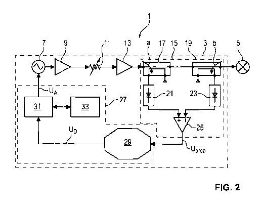
Figure 2 shows a schematic illustration of an embodiment of an RF system 1
according to the invention. The RF system 1 comprises an RF signal coupling-in
apparatus 3 and an RF device 5, which can be an RF lamp, an RF spark plug or
similar RF plasma application. The invention is described hereinafter purely
by
way of example on the basis of an RF lamp using the reference sign 5.
The RF signal coupling-in apparatus 3 serves for operating the RF lamp 5 and
for
this purpose generates an RF signal having an operating frequency for the
ignition and the operation of the RF lamp 5 by means of an oscillator 7. In
the
case of the embodiment of the RF system 1 according to the invention as shown
in Figure 2, an amplifier 9 and a damping element 11 are connected to the
oscillator 7, by means of which the output signal of the oscillator 7 can be
increased or reduced before it is increased to the operating power by means of
a
further amplifier 13. The amplifiers 9 and 13 and the damping element 11 are
optional and can either be omitted or be replaced by other suitable elements.
The
CA 02854589 2014-05-05
WO 2013/076174
PCT/EP2012/073292
8
arrangement in other combinations between the RF lamp 5 and the oscillator 7
is
also conceivable.
The RF signal coupling-in apparatus 3 additionally comprises means for
generating a voltage signal proportional to the degree of matching of the RF
device, said means being summarised with the reference sign 15. In accordance
with the embodiment of the invention as illustrated in Figure 2, said means 15
comprise two coupling-out devices 17 and 19, wherein the coupling-out device
17
serves for coupling out a portion a of the RF signal generated by the
oscillator 7,
while the coupling-out device 19 serves for coupling out a portion b of the
signal
reflected by the RF lamp 5. It goes without saying that a signal b is
reflected by
the RF lamp 5 only when the lamp is not optimally matched to the frequency of
the RF signal generated by the oscillator 7. The coupling-out device 17
therefore
serves for coupling out power running towards an RF lamp 5, while the coupling-
out device 19 serves for coupling out a power running away from, i.e.
reflected
by the RF lamp 5.
The means bearing the reference numeral 15 furthermore comprise a voltage
detection device 21 (detector), which serves for detecting and outputting a
voltage signal of the coupled-out portion a of the RF signal generated by the
oscillator 13. Furthermore, a voltage detection device 23 (detector) is
provided,
which serves for detecting and outputting a voltage signal of the coupled-out
portion of the signal b reflected by the RF lamp 5. In accordance with the
present
embodiment of the invention, the two voltage signals generated by the voltage
detection devices 21 and 23 are fed to a common operational amplifier 25,
which
generates a voltage Upro p proportional to the lamp matching on the basis of
the
output voltages of the voltage detection devices 21 and 23.
As an alternative to the embodiment of the means ¨ identified by the reference
number 15 ¨ for generating a voltage signal Uprop proportional to the degree
of
matching of the RF lamp, a circulator can be used instead of the coupling-out
devices 17 and 19, which circulator couples out the reflected signal of the RF
lamp 5 from the connection between the RF lamp 5 and the oscillator 7 and
makes it available as a controlled variable. However, the RF signal of the
oscillator 7 is lost in the process. In this case, either the operational
amplifier 25
can be dispensed with, or the latter can be replaced by an amplifier circuit.
In a
further embodiment of the means 15 for generating a voltage signal
proportional
CA 02854589 2014-05-05
WO 2013/076174
PCT/EP2012/073292
9
to the degree of matching of the RF lamp, provision can also be made for
providing only one coupling-out device 17 or 19, which can serve respectively
for
coupling out both the portion of the RF signal generated by the oscillator 7
and
the RF signal portion reflected by the lamp 5.
All that is crucial is that a device is provided which generates a voltage
signal
proportional to the degree of matching of the RF device from the RF signal of
the
oscillator 7 and the signal reflected at the lamp 5. In other words, the
generated
voltage signal proportional to the degree of matching of the RF device is a
measure of how much of the RF signal of the oscillator 7 that is passed to the
RF
lamp 5 is reflected at the RF lamp 5 and thus how high the mismatch of the RF
lamp is.
In a subsequent step, according to the invention, the voltage Uprop
proportional to
the lamp matching is fed to a preferably microprocessorless device 27 for
generating a control signal for matching the output frequency of the
oscillator 7.
In the case of the embodiment shown in Figure 2, the preferably
microprocessorless device 27 comprises an amplitude discriminator 29, a loop
filter 31 and a reset circuit 33. The amplitude discriminator 29 generates, on
the
basis of the voltage Uprop proportional to the degree of matching of the RF
lamp
5, a digital or clocked output voltage Up, which is in turn fed to a filter
device, in
particular to the loop filter 31, which smooths the clocked signal Up in such
a way
that a substantially analog output signal 14 is generated, which is fed to the
oscillator 7 as a control voltage. The control voltage UA fed to the
oscillator 7 is
thus a measure of whether the frequency of the oscillator 7 is to be
increased,
decreased or remain the same.
Figure 3 shows an exemplary embodiment of the so-called amplitude
discriminator 29 illustrated in Figure 2. The amplitude discriminator 29 has
an
input 35, at which the voltage Uprop proportional to the degree of matching of
the
RF lamp 5 is fed in. In the case of the present exemplary embodiment, a total
of
3 conditions K1, K2 and K3 are generated in the amplitude discriminator 29.
The
first condition K1 is generated on the basis of the voltage signal Uprop
proportional
to the degree of matching of the RF lamp 5 by means of said signal being
compared with a predefined voltage value. For this purpose, the amplitude
discriminator 29 comprises a comparator 39, to which first the voltage signal
Uprop
and secondly a fixed voltage value are fed, the latter being generated by a
CA 02854589 2014-05-05
WO 2013/076174
PCT/EP2012/073292
voltage value generating device 41. The voltage value generating device 41 is
preferably realized by a voltage divider. The comparator 39 compares the
present
value of the voltage Uprop with the fixed voltage value of the voltage value
generating device 41. The resulting output signal of the comparator 39
corresponds to the first condition Kl.
At the same time, in the amplitude discriminator 29, the voltage signal Uprop
is fed
to a differentiator unit 43 having an integrated inverted comparator, which
unit
derives the voltage signal Uprop. The output signal of the differentiator unit
43
thus provides information about the tendency of the lamp matching, that is to
say
whether the latter decreases or increases, and corresponds to the second
condition K2.
The first condition K1 and the second condition K2 are fed to a logic unit 45.
The
logic unit 45 is connected to a shift register, in particular to a 2-bit shift
register
47, which can be realized by two D-type flip-flops, for example, and receives
from them a third condition K3. As illustrated in Figure 3, the shift register
47 can
be connected to a clock generator 49 in order to artificially digitize or
clock the
analog process within the amplitude discriminator 29.
A possible realization of the logic unit 45 of the amplitude discriminator 29
is
illustrated in the schematic embodiment in accordance with Figure 4. The logic
unit 45 comprises three inputs 51, 53 and 55, wherein the first condition K1
is
fed to the logic unit 45 by the input 51, the second condition K2 via the
second
input 53 and the third condition K3 via the third input 55. The logic unit 45
furthermore comprises an output 57 connected to the shift register 47
illustrated
in Figure 3.
In the exemplary embodiment in accordance with Figure 4, the logic unit 45
comprises two logic gates 59 and 61 and an inverter 63. The logic gate 61 is
an
XOR gate, for example, while the logic gate 49 is an AND gate. The inverter 63
inverts the supplied signal of the XOR gate 61. If the output signal Y is
present at
the output 57 of the logic unit 45, the following holds true for the
arrangement
shown in Figure 4:
Y = K1 = (K2 @ K3)
CA 02854589 2014-05-05
WO 2013/076174
PCT/EP2012/073292
11
The logic unit 45 having the abovementioned relationship can be assigned to
the
truth table shown in Figure 5. It is evident from the truth table in
accordance
with Figure 5 that, in this embodiment, the output frequency of the oscillator
7 is
increased (Y=1) only when the voltage Uprop proportional to the lamp matching
from the operational amplifier 25 exceeds a value defined by the voltage value
generating device 41 and at the same time
- the condition K2 generated by the differentiator unit 43 having an
integrated inverting comparator is present (K2="1"), while the n-1 bit from
the shift register 47 corresponds to a "1"
- or the condition K2 generated by the differentiator unit 43 having an
integrated inverted comparator is not present (K2="0"), while the N-1 bit
from the shift register 47 corresponds to a "0".
The clock generator device 49 is advantageous because incorrect decisions on
account of a transient response of the individual logic gates can be avoided
thereby. A possible realization of the clock generator device 49 is
illustrated in
Figure 6. Shown by way of example, the clock generator device 49 comprises
there three inverters 65, 67 and 69, two resistors 71 and 73 and a capacitor
75,
in order to realize a signal at the output terminal 77 having a fixed
frequency f.
The following frequency arises for a resistance R for the resistors 71 and 73
and
a capacitance C for the capacitor 75:
f=0.558/(RC).
Figure 7 reveals an exemplary embodiment of the loop filter 31 illustrated in
Figure 2, said loop filter receiving a clocked output voltage Up from the
amplitude
discriminator 29. The loop filter 31 generates, from the digital control
signals of
the logic unit 45 passing via the shift register 47, an analog voltage for the
closed-loop control of the output frequency of the oscillator 7. In the
embodiment
in accordance with Figure 7, the loop filter 31 comprises a series resistor 79
and
at least one shunt capacitor 81 and also at least one shunt resistor 83, which
are
situated between the input terminal 85 connected to the shift register 47 and
the
output terminal 87, connected to the oscillator 7, of the loop filter 31.
CA 02854589 2014-05-05
WO 2013/076174
PCT/EP2012/073292
12
In order to increase the output frequency of the oscillator 7, the output 57
of the
logic unit 45 is set to "1". This signal charges the shunt capacitor 81 in the
loop
filter 31 via the series resistor 79 with a time constant Icharging that
corresponds to
the product of the resistance of the series resistor 79 and the capacitance of
the
shunt capacitor 81. The value "0" at the output 57 of the logic unit 45 has
the
effect that the charge on the shunt capacitor 81 is discharged via the
parallel
circuit formed by the shunt resistor 83 and the resistor 79. The corresponding
time constant Idischarge corresponds to the product of the capacitance of the
shunt
capacitor 81 and the resulting resistance of the parallel circuit formed by
the two
resistors 79 and 83.
Figure 8 shows a possible embodiment of the reset circuit 33 shown in Figure
2.
In this embodiment, the reset circuit 33 comprises a comparator 89 for
comparing
the voltage at the shunt capacitor 81 in the loop filter 31 with a reference
voltage
Ucomparativei wherein the reference voltage Ucomparative, can be generated by
means
of an external voltage divider 91, for example. The lower limiting frequency
of
the closed-loop control can thereby be defined. If the voltage at the shunt
capacitor 81 in the loop filter 31 falls below the voltage value Ucomparative,
a
voltage that charges the shunt capacitor 81 in the loop filter 31 is generated
via a
monostable switch 93. The output frequency of the oscillator 7 can thereby be
defined at an upper limiting frequency of the closed-loop control. The reset
circuit 33 and the resultant reset process can be activated as necessary both
during switch-on and during operation of the RF lamp 5.
To summarize, it can be stated that the RF system 1 shown in Figure 2 is
merely
an exemplary embodiment which can be modified with regard to some elements.
In particular, the coupling-out devices can be replaced by a circulator. The
voltage detection devices 21 and 23 can be suitable detectors of arbitrary
design.
Furthermore, there is the possibility of integrating the reset circuit 33
shown in
Figure 8 or the function of said reset circuit into the logic unit 45. On the
other
hand, there is the possibility of replacing the reset circuit 33 by gates, in
particular by comparators and/or simple Sample-and-Hold circuits.
The loop filter 31 in accordance with Figure 7 can, moreover, be replaced by
charge pumps, that is to say charge pump circuits based on the model of a
phase
locked loop circuit (PLL). In this case, the circuit can be designed such that
an
optimum operating frequency can be "held". In this case, the circuit is
somewhat
CA 02854589 2014-05-05
WO 2013/076174
PCT/EP2012/073292
13
more complex and larger and requires a new logic unit and negative voltages.
It
is also conceivable to integrate the loop filter 31 or at least the function
thereof
into the logic unit 45. An analog output voltage is then generated directly in
the
logic unit 45, such that the use of a clock generator is superfluous. It is
also
conceivable to extend the logic unit 45. In particular, further conditions can
be
taken into account, which can realize additional functions without the use of
a
microprocessor. Additional logic gates are then possibly necessary for this
purpose. Moreover, the shift register 47 can also be modified and in
particular
supplemented, for example by the use of astable flip-flops. In particular, it
is
possible to provide additional elements which make the clock generator or the
clock generator device 49 superfluous.
The use of amplifiers 9 and 12 and of the damping element 11 is also optional.
It
is also conceivable, for example, to use an amplifier having a variable gain
for
more exact power setting. Likewise, the damping element can be embodied in a
variable fashion or a corresponding additional variable damping element can be
provided. In particular, the order of amplification and damping is also
optional.
Overall, the present invention realizes an RF system and in particular an
advantageous RF signal coupling-in apparatus for use in an RF system for
coupling an RF signal into an RF device, in particular into an RF lamp, in a
manner as free of losses as possible. The RF signal coupling-in apparatus is
preferably of microprocessorless design and, rather, uses logic gates that
make a
microprocessor superfluous. In this way, the RF system realizes a fast analog
closed-loop control of the output frequency of an RF signal coupling-in
apparatus
e.g. for energy saving lamps. The RF signal coupling apparatus according to
the
invention enables ignition and efficient operation of an RF lamp at that
operating
frequency which has the best matching to the RF lamp. The advantageous analog
closed-loop control can furthermore compensate for frequency shifts caused by
the manufacturing tolerances, the operationally governed thermal behaviour or
ageing-dictated changes in the electronics. The logic unit implemented
consists of
individual logic gates and thus enables an advantageous integration of the
circuit
into a single semiconductor IC. It thus provides the prerequisites for a cost-
effective realization of the RF signal coupling-in apparatus and thus of the
entire
RF system using mass production.
CA 02854589 2014-05-05
WO 2013/076174
PCT/EP2012/073292
14
List of Reference Signs
1 RF system
3 RF signal coupling-in apparatus
RF device (RF lamp)
7 Oscillator
9 Amplifier
11 Damping element
13 Amplifier
Means for generating a voltage signal proportional to the degree of
matching of the RF device
17 Coupling-out device
19 Coupling-out device
21 Voltage detection device
23 Voltage detection device
Operational amplifier
27 Preferably microprocessorless device
29 Amplitude discriminator
31 Filter device (loop filter)
33 Reset circuit (reset device)
Input
37 Comparison device
39 Comparator
41 Voltage value generating device
43 Differentiator unit
Logic unit
47 Shift register
49 Clock generator device
51 Input
53 Input
Input
57 Output
59 Logic gate
61 Logic gate
63 Inverter
Inverter
67 Inverter
CA 02854589 2014-05-05
WO 2013/076174
PCT/EP2012/073292
69 Inverter
71 Resistor
73 Resistor
75 Capacitor
77 Output terminal
79 Series resistor
81 Shunt capacitor
83 Shunt resistor
85 Input
87 Output
89 Comparator
91 External voltage divider
93 Monostable switch
fo Operating frequency
fp' Shifted operating frequency
a Portion of the RF signal of the oscillator
b Portion of the reflected signal
Uprop Voltage proportional to the degree of matching of the lamp
Up Clocked output voltage
UA Analog output signal