Note: Descriptions are shown in the official language in which they were submitted.
CA 02854795 2014-05-06
WO 2013/070791
PCT/US2012/063977
ROOM TEMPERATURE GLASS-TO-GLASS, GLASS-TO-PLASTIC AND
GLASS-TO-CERAMIC/SEMICONDUCTOR BONDING
BACKGROUND INFORMATION
Field
[Para 1] Embodiments of the disclosure relate generally to the field of
bonding
of transparent substrates and more particularly to a method for room
temperature laser
bonding of a first laser wavelength transparent substrate to a second
substrate with an
intermediate heat absorption layer.
Background
[Para 2] Bonding of glass-to-glass substrates and other combinations of
transparent and non-transparent substrates for biological slides and
microfluidics
applications as well as other applications typically requires heating of the
substrates to
obtain bonding diffusion of the materials across the substrate boundaries
unless
adhesives are employed. Various examples of current bonding practices are
fusion
bonding, anodic bonding of sodium rich glass to semiconductors and adhesive
bonding.
[Para 3] Fusion bonding glass-to-glass is effective on polished or low
roughness glass surfaces. To achieve a strong, bubble free bond, typically the
surface
finish should be on the order of a few Angstrom RA. The process generally
involves
placing the two glass substrates in contact with each other and then applying
pressure
and heat. The pressure can range from the weight of the upper glass substrate
to a load
place on top of the glass. Special material must be used to prevent the weight
from
sticking to the glass. The bulk substrate is usually brought up to at least
the first
transition temperature (softening temperature) of the glass. For all practical
purposes,
the glass surfaces melt together and become one. This process is not very
robust
against environmental particles that are commonly found in a clean room
environment. A 50nm diameter particle, for example, will cause the glass not
to bond
-1-
CA 02854795 2014-05-06
WO 2013/070791
PCT/US2012/063977
in that particular area and cause a glass bubble which is apparent by the
presence of
Newton Rings.
[Para 4] This process can be assisted by treating the surface with ions
such as
calcium and activating the surface with Hydrofluoric Acid. Such treatments
tend to
lower the bonding temperatures but aggravate the contamination problem.
Contamination becomes more difficult because the particulate does not have the
ability to deform the glass such that the particle of contamination will
recess out of
the way and not hold the two surfaces apart.
[Para 5] Fusion bonding has two competing issues that cause a low yield;
the
glass surface must be absolutely clean in order to not create air bubbles at
low
temperatures, and when higher temperatures are used, while air gaps become
less a
problem, the surface of the glass becomes distorted and must be reprocessed in
order
to make it optically clear again. Higher temperatures can also cause the glass
to
become hazed or yellowish.
[Para 6] While there are a few exceptions, it is generally not possible to
bond
glass-to-glass with an Anodic bonding process. This process is usually
reserved for
bonding glass to silicon. Anodic bonding is usually performed using glass
substrate
with sodium as one of its constituents. The temperature is generally elevated
to
approximately 400 degrees Celsius. A potential difference is then applied to
drive the
sodium atoms across the boundary of the glass-silicon assembly. This process
creates
a sodium-oxide bond across the boundary. This process usually leaves the
surface of
the glass transparent and smooth. However, it is assumed that the bonding
process is
taking place near a channel, the depletion of the sodium atoms from the
surface of the
glass near the bonded interface layer, leave the glass sodium rich. This
surface is then
positively charged. Such a charge on the surface of the glass can easily
interfere with
downstream processes during the use of the chip.
[Para 7] There are adhesives specifically designed to bond glass to glass.
While
adhesive is easy to apply, it is very hard to make a bubble free joint. It is
also very
hard to pattern adhesive such that the bond line is complete but does not
squeeze out
from between the surfaces being bonded and into a neighboring channel.
Adhesives
-2-
CA 02854795 2014-05-06
WO 2013/070791
PCT/US2012/063977
can be hazardous to the downstream process. Certain adhesive compositions can
kill
the biology that the component is being made to house.
[Para 8] Each of the above bonding processes does not render a chemically
inert bonding process. In each case the bond lines are not robust against
strong
concentrations of acid or bases. They will tend to etch at a much higher rate
than that
of the bulk surface. The higher etch rate can cause small crevasse that are
hard to
clean or harm the flow of liquid in the channel assembly in the case of micro-
fluidics.
[Para 9] Because each of the above typically require heat, it is necessary
to
match the thermal-coefficient-of-expansion of each material. If this is not
done, when
the material returns to room temperature the bonded component will warp and/or
break. The adhesive joint will fail in shear or peel if the use temperature is
different
from the bonding temperature; adhesive shear strength is usually low.
[Para 1 0] It is therefore desirable to provide a glass-to-glass or other
substrate
bonding process providing bonding times in a range of minutes as opposed to
hours
for anodic bonding or heat diffusion bonding. It is further desirable to
provide a
bonding process with a tolerance to dirt, which can bond through 100nm
diameter
particles. It is also desirable that the bonding process provide a selectable
width bond-
line width 10 to 100p.m with bonded un-bonded discrimination of 1p.m.
Additionally,
it is desirable that the bonding process is inert and does not over etch in
HF/Sulfuric/KOH (as with diffusion bonding) and does not change the charge on
the
surface of the glass as with anodic bonding. It is also desirable that the
bond-line is
virtually transparent and the bonding process can structure the bond line as
well as
conductors and non-conductors within the bonded structure on the same surface.
Finally, it is desirable that bonding can be accomplished on a fluidic device
loaded
with live cultures such as yeast, anthrax or other biological materials
without harming
them.
SUMMARY
[Para 11] Embodiments disclosed herein provide a process for room
temperature
substrate bonding in which a first substrate substantially transparent to a
laser
wavelength is selected. A second substrate for mating at an interface with the
first
-3-
CA 02854795 2014-05-06
WO 2013/070791
PCT/US2012/063977
substrate is then selected. A change in index of transmission is created at
the interface
and the first and second substrates are mated at the interface. The first
substrate is
then irradiated with a laser of the transparency wavelength substantially
focused at the
interface and a localized high temperature at the interface from energy
supplied by the
laser is created. The first and second substrates immediately adjacent the
interface are
softened with diffusion across the interface to fuse the substrates.
[Para 1 2] In example embodiments, the trasnsmissivity change may be
accomplished by deposition of a blocking heat absorption coating on the
surface of
one substrate at the interface. In alternative embodiments, the transmissivity
change
may be accomplished by differing transmissivity of the substrates themselves.
[Para 1 3] An example embodiment for an apparatus for room temperature
laser
bonding incorporates an x-axis motion stage mounted to a base and a y-axis
motion
stage mounted to the x-axis motion stage. A substrate alignment fixture is
mounted on
the y-axis motion stage adapted to align and secure at least two substrates
with a
mutual interface as a workpiece. A gantry is mounted to the base and supports
alignment optics for a laser to focus on the workpiece in the alignment
fixture. A
controller provides for translation of the x-axis motion stage and y-axis
motion stage
for motion of the focused laser on the workpiece.
[Para 14] The features, functions, and advantages that have been discussed
can
be achieved independently in various embodiments of the present disclosure or
may
be combined in yet other embodiments further details of which can be seen with
reference to the following description and drawings.
BRIEF DESCRIPTION OF THE DRAWINGS
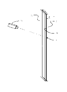
[Para 1 5] FIG. 1 is a pictorial schematic representation of one
embodiment;
[Para 16] FIG. 2 is a flow chart of the method for room temperature
substrate
bonding;
[Para 1 7] FIG. 3A is a pictorial view of a fixturing and translation
system for
holding mated substrates and providing laser path guidance;
[Para 1 8] FIG. 3B is a detail view of the substrate alignment fixture;
-4-
CA 02854795 2014-05-06
WO 2013/070791
PCT/US2012/063977
[Para 19] FIG. 3C is an exploded view of the alignment fixture of FIG. 3B;
[Para 20] FIG. 3D is a detail view of the substrate holding frame;
[Para 21] FIG. 3E is an exploded view of the substrate holding fame;
[Para 22] FIG. 4 is a flow chart of process control steps for room
temperature
substrate bonding; and,
[Para 23] FIG. 5 is a flow chart of an example embodiment for processing of
leads integrally with bonding of the substrates.
DETAILED DESCRIPTION
[Para 24] Embodiments disclosed herein provide a method and apparatus for
bonding of similar substrates such as glass-to-glass and dissimilar substrates
such as
glass-to-glass (with differing material properties such as coefficient of
thermal
expansion (CTE)), glass to plastic, glass to silicon and glass to ceramic.
Referring to
FIG. 1, bonding of the substrates 10, 12 is accomplished using a laser 14
which has a
wavelength such that at least one of the substrates (substrate 10 for the
example
shown) is transparent to that wavelength. An interface 15 between the layers
provides
a change in the index of transmission or optical transmissivity which results
in
absorption of laser energy at the interface and localized heating to create a
bond. In a
first embodiment, a heat absorption layer 16, which is opaque or blocking to
the laser
wavelength and has an affinity for diffusion into the substrates, is deposited
on the
mating surface 18 of at least one of the substrates (substrate 12 for the
example
shown). The heat absorption layer in example embodiments for glass-to-glass
and
other substrate bonding herein may be a metal, semiconductor or ceramic
material.
However, in alternative embodiments other materials having appropriate
wavelength
absorption and diffusion affinity characteristics may be employed. The
thickness of
the heat absorption layer may be as thin as 10A and as thick as desired to
compensate
for surface roughness or control timing and temperatures of the process as
will be
described in greater detail subsequently.
[Para 25] The desired change in transmissivity at the interface can also be
accomplished through the use of substrate materials having one substrate which
is
-5-
CA 02854795 2014-05-06
WO 2013/070791
PCT/US2012/063977
opaque (low transmissivity to the laser wavelength) or a liquid film having a
mismatched index of transmission from the initial substrate.
[Para 26] The bonding process is accomplished as shown in FIG. 2 with
reference to the elements disclosed in FIG. 1 for a first example of a glass-
to-glass
bond wherein a glass substrate 10 of any type generally transparent to the
wavelength
of the laser 14 being used is selected as the first substrate, 202. A change
in
tansmissivity is created at the interface 15, using, for the example of the
first
embodiment, a heat absorption layer 16 applied to either the first substrate
10 or the
second substrate 12 to be bonded, 204. The heat absorption layer may be
continuous
or segmented strips surrounding features in the substrates such as
microfluidic
channels. The two substrates are then placed in contact with each other with
the heat
absorption layer being placed such that it is in the interface between the two
substrates, 206. The surfaces may or may not be extremely well polished. The
thickness of the heat absorption layer can be thickened to compensate for
surface
roughness. The assembled substrates are then clamped in a fixture, to be
described in
greater detail subsequently, that is transparent to the wavelength of laser
energy being
used, 208. The laser is then roughly focused on the interface of the assembled
substrates in the fixture, 210. The laser energy is then applied to the
substrates being
bonded, 212.
[Para 27] The laser energy penetrates the first substrate 12 and impinges
on the
heat absorption layer, 214. The heat absorption layer will continue to absorb
the
energy until a plasma is formed and the temperature of the heat absorption
layer is
raised to a diffusion temperature, 216. However, before the absorption layer
diffuses,
the glass surfaces in near proximity to the surface to the heat absorption
layer soften,
218, until the heat absorption layer diffuses into the glass, 220. Upon
diffusion into
the glass, the material from the heat absorption layer becomes transparent to
the laser
energy, 222. Once the heat absorption layer diffuses the plasma collapses and
the
softened glass fuses together into a permanent bonded joint, 224. It is
important to
note that the heat absorption layer should diffuse at temperature that is
higher than the
first transition temperature of the glass to ensure that the glass becomes
soft and
-6-
CA 02854795 2014-05-06
WO 2013/070791
PCT/US2012/063977
bonds to the neighboring glass. This approach makes the most robust, least
particulate
sensitive bond joint.
[Para 28] In this first example of a glass-to-glass bond, the entire
process takes
place such that the bulk material remains at room temperature and only the
heat
absorption layer and the materials of the substrates immediately adjacent the
bond-
line itself arc elevated to a temperature where the heat absorption layer is
diffused into
the glass by the laser. The width of a single bond-line can vary from
approximately
0.0014m to 100 um or greater and the depth of the bond-line is nominally 500nm
into each component of the structure. However, it can vary from a fraction of
a micro-
meter to multiple micro-meters.
[Para 29] The disclosed process takes advantage of the affinity of metals,
ceramics and semiconductors to diffuse into glass at elevated temperatures
making the
bond-line virtually transparent both in the visible spectrum and to the laser
radiation
wavelength. Therefore, the process is self-regulating. When the absorption
layer has
fully diffused into the glass, the laser energy passes through the glass with
no further
heating and the reaction stops. Therefore, the glass is never ablated or over-
heated by
the laser.
[Para 30] The material transparency, for the substrate(s) which the laser
passes
through, should be at least 70 percent at the wavelength at the laser energy
wavelength. This allows sufficient power penetration through glass to the
depth of the
heat absorption layer. If the laser radiation is absorbed, the glass may crack
and
absorption layer may not be diffused resulting in an incomplete bond or no
bond at
all. While laser-transparency is desirable for the layer that the laser passes
through, it
may not be necessary for the second substrate in the stack to be effectively
bonded to
the first substrate.
[Para 31] An example fixture for support of the mated substrates during
laser
bonding processing is shown in FIGs. 3A ¨ 3D. A positioning system 30
incorporates
an x-axis motion stage 32 mounted on a base 33 and a y-axis motion stage 34
mounted to the x-axis mounting stage. For the embodiment shown, a substrate
alignment fixture 36 is mounted on the y-axis motion stage. However, in
alternative
-7-
CA 02854795 2014-05-06
WO 2013/070791
PCT/US2012/063977
embodiments, the motion stages may be reversed in vertical stacking and the
alignment fixture mounted on the x-axis stage. Each motion stage has a drive
motor
38 with associated screw drive 40 or similar translation mechanism. Covers 42
shield
the operating elements of the motion stages for operator safety. A gantry 44
provides
support for alignment optics 46 for the laser 14, final focusing optics 48,
camera 50
and other instrumentation systems as required for monitoring and control of
the
bonding operation. For the embodiment shown, a power meter 52 is mounted to
the
x-axis motion stage to be positioned under the laser optical train for
measurement
and/or calibration of laser power before movement of the alignment fixture
under the
laser optics for substrate bonding. In the embodiment shown, a z-axis motion
stage 54
is provided for vertical positioning of the optical and measurement systems
with
respect to the alignment fixture. A computer controller 55 is programmable for
translation of the x-axis, y-axis and z-axis motion stages for translation of
the laser on
the workpiece. A single laser may be employed for illuminating multiple
substrate
work pieces in individual positioning systems by employing beam splitters and
focusing optical trains to the multiple positioning systems. It is also
possible to
replace the fixed lens with an f-theta lens with an X-Y scanner and Z-auto-
focus
either by itself or in conjunction with a large travel X-Y positioning system.
[Para 32] Details of the alignment fixture 36 are shown in FIGs. 3B and 3C.
A
mounting structure 56 is provided to mount the alignment fixture to the y-axis
stage.
For the embodiment shown the mounting structure is fabricated from attachment
plate
58, spacer 60 and engagement support plate 62. A vertically translating
engagement
slider 64 is supported by translation rods 66 received in bushings 67. A
pneumatic
expansion device 68 positioned intermediate the engagement slider 64 and
engagement support plate 62 provides vertical adjustment of the engagement
slider as
will be described subsequently. A workpiece holding frame 70 supports a
workpiece
71 consisting of the mated substrates 10, 12 as will be described in detail
with respect
to FIG. 3C. Risers 72 extend upward from the engagement support plate 62 to
receive
an optical flat 74 to be positioned over the holding frame. A securing plate
76
-8-
CA 02854795 2014-05-06
WO 2013/070791
PCT/US2012/063977
mounted with spacers 78 fixes the optical flat to the risers. The optical flat
is
transparent to the laser and may be a fused silica or similar material.
[Para 33] Deflation of the pneumatic expansion device 68 lowers the
engagement slider 64 allowing insertion of the holding frame 70 into position
on the
engagement slider. A receiving frame 79 positions the holding frame. Inflation
of the
pneumatic expansion device urges the engagement slider and holding frame
upward
compressing the substrate 10 against the optical flat 74.
[Para 34] The holding frame 70, as shown in F1Gs. 3D and 3E, includes a
base
80, a clamping structure 82 and a substrate carrier 84. The clamping structure
incorporates a casing 86 which carries a lateral clamp 88 and a longitudinal
clamp 90.
The substrate carrier 84 has a relief 92 sized to closely receive the
substrates 10, 12
supporting the lower substrate on a compliant surface 94 integral to or
inserted in the
relief 92. A silicon rubber or similar material may be employed for the
compliant
surface to provide resilient clamping of the substrates against the optical
flat after
inflation of the pneumatic expansion device. The lateral clamp 88, for the
embodiment shown incorporates two vertical arms 96 which extend through
slotted
apertures 98 in the substrate carrier adjacent the relief 92. The lateral
clamp is spring
loaded to allow outward displacement of the arms 96 by depressing button 100
for
insertion of the substrates into the relief. Upon releasing button 100, the
arms engage
the sides of the substrates and urge the substrates against the wall of the
relief
opposite the slotted apertures. Similarly, the longitudinal clamp 90 has a
single arm
102 extending through a slotted aperture 104 in the substrate carrier adjacent
the relief
92. The longitudinal clamp is spring loaded to allow outward displacement of
the arm
102 by depressing button 106 for insertion of the substrates into the relief.
Upon
releasing button 106, the arm engages the ends of the substrates and urges the
substrates against the wall of the relief opposite the slotted aperture. The
substrates
are securely positioned against two perpendicular surfaces of the relief
[Para 35] The alignment fixture 36 mounted on the x-axis motion stage 42
and y-
axis motion stage 44 allows translation of the substrate workpiece 71 under
the laser
beam emitted from the final optics for exposing the heat absorption layer. A
tracking
-9-
CA 02854795 2014-05-06
WO 2013/070791
PCT/US2012/063977
path may be programmed into the controller 55 for motion stages attached to
the
holding tool to allow the laser beam impinging on the mated substrates to
follow
features in the substrates such as microfluidic channels, shown as step 213 in
FIG. 2.
While translation of the substrate holding fixture is employed for the
embodiment
described, alternative embodiments may employ a stationary hold fixture with
translating motion of the laser or laser beam through optical means.
[Para 36] A laser light trap is required in the bonding fixture such that
the laser
energy does not burn the fixture or reflect and damage some other aspect of
the
component. For the disclosed embodiment, the silicon rubber compliant surface
94
absorbs the laser and does not burn. A polytetrafluoroethelyne (PTFE) layer
such as
Teflon could alternatively be employed or physically defined light traps
under the
glass chip such as those offered by Thorlabs, 435 Route 206 North Newton, NJ
07860 may be incorporated into the fixture.
[Para 37] Additional examples of the process are provided below.
EXAMPLE 1 Substrates of Different Thermal Coefficient of Expansion (TCE):
[Para 38] Traditional bonding processes typically occur at elevated
temperatures,
where a vastly different TCE generates severe temperature distortion when the
bonded assembly cools down. However, with laser bonding process disclosed
herein
it is possible to bond dissimilar TCE materials at the temperature. Since the
bulk
temperature of the material being bonded can be set at the temperature of use,
the
TCE while still being different does not stress or otherwise distort the
substrate
material because it does not see a temperature change.
[Para 39] For example when fusion bonding two substrates that are 150mm in
diameter with a TCE that differs by 7ppm/ C at a temperature of 100 C. The
differential change in length from the top to the bottom substrate causes an
engineering strain of 0.07% translating into a tensile stress in the bottom
substrate of
54.6Mpa (7.92 kpsi). Most glasses, for example, will fail in tension between 1
to 2
kpsi when not stabilized.
[Para 40] When anodic bonding 7ppm/ C glass to silicon, it is common for
the
bonding temperature of the glass to be 400 C. Such a temperature will cause a
tensile
stress of over 200Mpa. This will fracture the glass. However, a room
temperature laser
bonded substrate stack employing the process described will never be exposed
to such a
large change in temperature and therefore, will not fracture during the
process of bonding.
Post bonding, the substrates, which may be in the form of wafers, will be
diced into
smaller components. When length reduction occurs, the stress is reduce by the
length
reduction of the component as compared to the length of the wafer, i.e., a
component that
will see a 100 C that is 10 mm long will experience a stress of 5.5 Mpa (0.8
kpi). Glass
will very easily survive this stress.
EXAMPLE 2 Different Light Transmission at a Similar Laser Radiation Wave
Length
[Para 41] It is a common practice to bond glass packaging to a silicon
chip. When
performing this process, it is usually necessary to match the CTE of each of
the materials
and to use a glass material with sodium atoms that can migrate during the
elevated
temperature bonding process. While there are commercially available glass
materials that
exhibit such properties. they are hard to process during such steps as
introducing a via.
Photo-sensitive glass ceramic material, such as ForturanTM, is easy to
structure; however,
it has a CTE of lOppm/ C and does not contain sodium ions. These two
attributes make it
nearly impossible to anodic bond to silicon. While it can be fusion bonded, it
requires
being heated to 500 C. Such a high temperature change will cause the glass-
silicon
assembly to fracture during the cool down process.
[Para 42] While diffusion or Anodic bonding ForturanTM to Silicon is not
practical,
the laser bond process described herein may be employed for structured
Forturaem to
silicon or many other ceramics or metals. Since the process of room
temperature laser
bonding requires a transmissivity change at the interface for creating a heat
absorption
layer, a transparent plate of glass to a second substrate or blocking plate of
material
opaque to the laser wave length is employed in much the same manner as for two
transparent substrates. However, when bonding a full blocking plate to a
transparent plate
the process will not be self-regulating and requires that the process must be
very carefully
controlled such that the blocking plate does not get exposed to so much power
that the
surface becomes ablated. This is done by controlling the laser fluence such
that the
surface of the second substrate at the interface is heated to well beyond
-11-
CA 2854795 2019-04-04
CA 02854795 2014-05-06
WO 2013/070791
PCT/US2012/063977
the first transition temperature of the glass, such that the glass softens
under the laser
radiation being absorbed by the second substrate. This will ensure that during
the
cooling process silicon dioxide bonds will form at the interface and adhere
each of the
components to each other. This process functions with glass to silicon, glass
to
ceramics, glass to metals and glass to plastics bonding.
[Para 43] An example of process control for the laser bonding process when
applied to materials as in Example 2 is shown in FIG. 4 wherein the initial
step is
selecting the material for the blocking heat absorption layer, 402. A layer of
the
blocking heat absorption material is then deposited in a layer of a thickness
such that
thermal diffusion length (Lf) is less than the optical penetration depth (a-
1), 404. The
layer may be deposited on either the first or second substrate on the
interfacing
surface. A laser radiation wave length is then selected for a transmission of
greater
than 70%, 406. A laser radiation pulse width is selected consistent with the
thermal
diffusion length (Lf), 408. A laser radiation power is selected such that the
blocking
layer vaporization point is achieved, 410. The stage translation rate for the
holding
tool is controlled to ensure that at the laser radiation pulse rate less than
a 50% pulse
to pulse overlap is present, 412. The holding tool is then translated to
achieve the
desired laser path on the mated substrates to effect the bond, 414.
EXAMPLE 3 Glass-to-Plastic Bonding:
[Para 44] Glass to plastic bonding is very similar to the above process
with one
limitation; the blocking layer should be a relatively low temperature
diffusion
material such that it does not melt the polymer being attached to the glass. A
particularly good material with a low diffusion temperature is AuSn (gold-tin
eutectic). A gold-tin blocking heat absorption layer has a diffusion
temperature of
280 C. Another helpful attribute is that the laser-pulse-width approaches the
thermal-
time-constant of the blocking heat absorption layer layer, i.e., in the femto-
second
regime. The shorter the pulse length, the less likelihood there is to burn or
melt the
polymer prior to bonding the high-melting-temperature glass material to the
lower
temperature melting plastic material. It is also possible to use infared laser
radiation
-12-
CA 02854795 2014-05-06
WO 2013/070791
PCT/US2012/063977
without an interlayer and use the blocking nature of the polymer at this
wavelength to
perform the bonding.
EXAMPLE 4 Silicon to Glass Bonding:
[Para 45] In the previous process descriptions, the laser transmission
wavelength
was selected such that the laser light was allowed to transmit through the
visibly
transparent substrate to the visibly blocking substrate. However, this is not
always
possible, desired nor is it required. For example, silicon has a 55% light
transmission
between lum and 10um wave lengths while Bk-7 glass has a near zero
transmission
above a 3um wave length. This makes it possible to use a CO2 laser to
penetrate the
silicon but not the glass. Such a process can be used to perform silicon back
side
attach to the front side of glass while aligning the laser on the bond
location at the
interface between the substrates. The laser is going through the silicon,
hitting the
glass/metal blocking layer and bonding.
[Para 46] Under certain circumstances, such as providing bonding of
substrates
with pre-filled microfluidic channels, it is necessary or desirable to pre-
coat or pre-fill
the substrate surfaces or channels in one or both the substrates with either a
lOnm to
100nm thick coating or a bioactive fluid respectively. With current bonding
processes
that heat the substrates over room temperature, the films or fluids will
either be
carburized or super-heated thereby destroying the films, boiling off the fluid
and
killing the live culture. The laser bonding process described herein does not
raise the
temperature of the bulk substrate and therefore, does not damage the surface
coating,
boil the fluid in the channels or kill the active culture. The heat affected
zone from
laser bonding is approximately lum. It has also been shown to bond through
100nm
thick layers of Teflon, Paraline and other polymers.
[Para 47] Additionally, a unique attribute of the room-temperature laser
bonding
process described herein is the ability to form structure conductive leads
into the same
interface layer that is being bonded. The structure of the leads is formed by
the laser
track on the mated substrates at the time of bonding. Therefore, it is not
necessary to
pattern the bonding layer to create a contact lead structure. This also makes
for a very
green process by avoiding currently required deposition and etching processes.
-13-
CA 02854795 2014-05-06
WO 2013/070791
PCT/US2012/063977
[Para 48] For example, if an array of electrolysis channels requires
multiple
connections to each channel to drive the process, the connections may be
formed
coincident with the bonding process. As shown in FIG. 5, the entire first
substrate is
metalized, 502, and used as an etch-stop layer. The channel would then be
patterned
and etched, 504. The etch mask is then removed while the metal layer remains,
506.
The metal layer constitutes the blocking heat absorbing layer. The fully
metalized first
substrate is then assembled with a capping second substrate that may or may
not be
structured with an inlet and outlet via, 508. The capping second substrate
assembled
with the channeled first substrate is then laser bonded together with
translation on the
predetermined path for laser impingement leaving undiffused metal traces to
form
leads that pass right through the interface layer, 510.
[Para 49] The leads do not leak, even though they pass through the bond
interface because the bonding process put the interface in compression when it
cools.
This causes the channel substrate to clamp down on the surface substrate
creating a
tight seal. When the lead needs to be wide, the lead can be divided into
sections such
that the compression is applied to a narrow strip but the lead itself remains
conductively wide. It is also possible to bond the traces to the adjacent
glass without
totally diffusing the metal into the glass. The undiffused metal traces may be
laser
bonded with a shorter pulse length and therefore would bond but not fully
diffuse the
layer of metal into the glass. Leaving the glass bonded but yet conductive.
[Para 50] Finally this process can act upon multiple substrate interfaces
at the
same time. Because the laser process is self-regulating and substrates and the
blocking
heat absorption layer become transparent to the laser radiation upon diffusion
of the
heat absorption layer, the laser will pass through the first interface to the
next
interface and bond it at the same time. While it is not necessary to limit the
number
of interfaces to a particular number, experiential data indicates that as many
layers as
seven interfaces can be bonded at one time while leaving contact leads within
each
interface.
[Para 51] For the embodiments described, when bonding one substrate to
another, it is best to begin with at least a 100nm Ra surface finish on
interfacing
-14-
CA 02854795 2014-05-06
WO 2013/070791
PCT/US2012/063977
surface of each substrate to be bonded. It is possible for the substrates to
be as rough
as lum Ra; however, the hermitic nature of the bond will be questionable
unless the
blocking/metal layer is substantially thicker. The substrate must be cleaned
and free
of debris as is the case with anodic or fusion bonding. However, since this
bonding
process does not require being 100% bonded over the entire surface but rather
can be
seam sealed, the statistics of a good bond are weighted in the direction of a
greater
yield than that of a typical bonding process.
[Para 52] When bonding two transparent substrates, it is necessary to apply
a
metallic/blocking layer on the surface of one of the substrates. For a typical
4A Ra
surface finish, 100nm of Cr is sufficient as a blocking heat absorption layer.
[Para 53] The substrates should be clean to a suggested sub-100nm
particle/10mm contamination before being assembled with the blocking layer
disposed toward the adjacent transparent substrate. In the case of thin
substrates, it is
necessary to apply pressure to the outer surfaces of the each substrate
thereby,
clamping the substrates together such that no gaps exist between them.
Clamping can
take place using physical external contact force as described for the example
support
fixtures or by applying a vacuum to draw that air out from between the
surfaces of the
substrates.
[Para 54] When using a physical clamp, a compliant layer, such as silicone
rubber, is disposed on the outer surface of one substrate and a relatively
hard (fused
silica), transparent surface on the opposing outer substrate. Example
embodiments
employ 138kPa (20psi) as a sufficient amount of pressure to ensure intimate
contact
between the inside adjacent surfaces.
[Para 55] When applying a vacuum for clamping thicker substrates, one can
use
the process known in the art of a typical wafer aligner. However, a blanket
expose
light is not used to expose a light sensitive chemical, but rather, a laser is
used to
diffuse the blocking layer.
[Para 56] With the substrate surfaces in close contact, the assembled
workpiece
can be loaded into a motion platform of the type whereby either the stage
positions
the substrate under the laser beam or whereby a scanner using an f-theta lens
positions
-15-
CA 02854795 2014-05-06
WO 2013/070791
PCT/US2012/063977
the beam over the substrate; either process can be adopted for the purpose of
precision
or speed, respectively.
[Para 57] Control software is required to position the stage, scanner or
stage/scanner assembly. For example embodiments, three dimensional computer
aided
design software creates the bonding path, which is then translated into G-code
by
computer aided manufacturing software and then again is post processes it into
motion board position commands.
[Para 58] When bonding thin substrates, care must be taken to not over
write the
previously bonded path. This is because the transmission of the laser through
the
substrate changes once the blocking layer is absorbed into the glass.
Typically, the
transmission is reduced and therefore will cause the substrate to absorb
enough laser
energy to cause a local rise in temperature (under the laser radiation beam)
and
thereby cause undue stress, due to the CTE of the material, in the thinner
substrate
and potentially fracture the assembly. Since a laser radiation beam, that does
pass
through an aperture, typically has a Gaussian distribution, it is best to
interleave the
space between the tail and the main beam of a first pass with the tail of a
second pass.
This will usually ensure that the substrate will not fracture.
[Para 59] Having now described various embodiments of the disclosure in
detail
as required by the patent statutes, those skilled in the art will recognize
modifications
and substitutions to the specific embodiments disclosed herein. Such
modifications
are within the scope and intent of the present disclosure as defined in the
following
claims.
-16-