Note: Descriptions are shown in the official language in which they were submitted.
CA 02855325 2014-06-26
267455
METAL-OXIDE-SEMICONDUCTOR (MOS) DEVICES WITH INCREASED
CHANNEL PERIPHERY AND METHODS OF MANUFACTURE
BACKGROUND
100011 The subject matter disclosed herein relates to metal-oxide-
semiconductor (MOS)
devices, such as silicon carbide (SiC) power devices (e.g., MOSFETs, IGBTs,
etc.).
[0002] This section is intended to introduce the reader to various aspects of
art that may
be related to various aspects of the present disclosure, which are described
and/or claimed
below. This discussion is believed to be helpful in providing the reader with
background
information to facilitate a better understanding of the various aspects of the
present
disclosure. Accordingly, it should be understood that these statements are to
be read in
this light, and not as admissions of prior art.
100031 Power electronics systems are widely used throughout modern electrical
systems
to convert electrical power from one form to another form for consumption by a
load.
Many power electronics systems utilize various semiconductor devices and
components,
such as thyristors, diodes, and various types of transistors (e.g., metal-
oxide-
semiconductor field-effect transistor (MOSFETs), junction gate field-effect
transistor
(JFETs), insulated gate bipolar transistors (IGBTs), and other suitable
transistors), in this
power conversion process.
100041 Specifically for high-voltage and/or high-current applications, devices
utilizing
wide bandgap semiconductors, such as silicon carbide (SiC), aluminum nitride
(AIN),
gallium nitride (GaN), etc., may afford a number of advantages in terms of
high
temperature operation, reduced ON-resistance, and smaller die size than
corresponding
silicon (Si) devices. Accordingly, wide bandgap semiconductor devices offer
advantages
to electrical conversion applications including, for example, power
distribution systems
(e.g., in electrical grids), power generation systems (e.g., in solar and wind
converters), as
well as consumer goods (e.g., electric vehicles, appliances, power supplies,
etc.).
CA 02855325 2014-06-26
267455
However, the differences between SiC and Si material systems, for example, can
cause
certain material processing and structural features (e.g., device designs
and/or
manufacturing processes) that work well for Si devices to be unsuitable for
corresponding
SiC semiconductor devices, and vice versa. Accordingly, in addition to their
benefits,
wide-bandgap semiconductor materials also present challenges during device
design and
fabrication.
BRIEF DESCRIPTION
[0005] Certain embodiments commensurate in scope with the originally claimed
subject
matter are summarized below. These embodiments are not intended to limit the
scope of
the claimed invention, but rather these embodiments are intended only to
provide a brief
summary of possible forms of the invention. Indeed, the present disclosure may
encompass a variety of forms that may be similar to or different from the
embodiments
set forth below.
[0006] In an embodiment, a semiconductor device includes a silicon carbide
(SiC) drift
layer disposed on a (0001) oriented SiC substrate. The SiC drift layer has a
non-planar
surface including a plurality of repeating features that are oriented parallel
to a channel
region of the semiconductor device. Further, the channel region is disposed in
a
particular crystallographic plane of the SiC drift layer.
[0007] In another embodiment, a method of manufacturing a semiconductor device
includes forming a non-planar surface on top of a silicon carbide (SiC) drift
layer,
wherein the non-planar surface includes a plurality of repeating features
having sidewalls
oriented along a 03-6 } plane, a {1120 } plane, or a 1
plane of the SiC drift layer.
The method includes forming a non-planar well region from at least a portion
of the non-
planar surface of the SiC drift layer and forming a non-planar n+ or p+ region
from at
least a portion the non-planar well region.
[0008] In another embodiment, a semiconductor device includes a silicon
carbide (SiC)
drift layer disposed on a (0001) oriented SiC substrate. The SiC drift layer
has a non-
2
CA 02855325 2014-06-26
267455
planar surface with a plurality of repeating triangular or rectangular
features that have
sidewalls configured to dispose a channel region of the semiconductor device
in a
crystallographic plane of the SiC drift layer, such as a {O'3i3-} plane, a
I plane, or
a {1100 } plane of the SiC drift layer. Further, the repeating triangular or
rectangular
features have a dopant concentration that is greater than a dopant
concentration in a
remainder of the SiC drift layer.
BRIEF DESCRIPTION OF THE DRAWINGS
[0009] These and other features, aspects, and advantages of the present
invention will
become better understood when the following detailed description is read with
reference
to the accompanying drawings in which like characters represent like parts
throughout the
drawings, wherein:
[0010] FIG. 1 is a schematic of a typical planar MOSFET device;
[0011] FIG. 2 is a schematic illustrating resistances for various regions of a
typical
MOSFET device;
[0012] FIG. 3 is a schematic of a vertical non-planar MOSFET device having a
triangular
wave device profile, in accordance with an embodiment of the present approach;
[0013] FIG. 4 is a schematic of a non-planar lateral MOSFET device having a
triangular
wave device profile, in accordance with an embodiment of the present approach;
[0014] FIG. 5 is a schematic of a non-planar MOSFET device having a square
wave
device profile, in accordance with an embodiment of the present approach;
[0015] FIG. 6 is a schematic of a non-planar MOSFET device having a sine wave
device
profile, in accordance with an embodiment of the present approach;
[0016] FIGs. 7A-7D are diagrams illustrating particular crystallographic
planes of a
hexagonal SiC crystal (e.g., 4H-SiC, 6-H-SiC);
3
CA 02855325 2014-06-26
267455
[0017] FIG. 8 is a graph illustrating drain characteristics for a planar SiC
MOSFET
device, an embodiment. of a non-planar SiC MOSFET device, and an embodiment of
a
non-planar SiC MOSFET device having a channel disposed along a particular
crystallographic plane;
[0018] FIG. 9 is a graph illustrating reverse current-voltage (IV)
characteristics for a
planar MOSFET device and an embodiment of a non-planar MOSFET device;
[0019] FIG. 10 is a cross-sectional view of the MOSFET device of FIG. 3, in
accordance
with an embodiment of the present approach;
100201 FIG. 11 is a cross-sectional view of an embodiment of the MOSFET device
of
FIG. 3 having deeper trench features and higher doping in the drift region
between the
trench features (e.g., compared to the doping of the drift layer below the p-
/n-well);
[0021] FIG. 12 is a cross-sectional view of the MOSFET device of FIG. 5, in
accordance
with an embodiment of the present approach;
[0022] FIG. 13 is a cross-sectional view of an embodiment of the MOSFET device
of
FIG. 5 having deeper trench features and higher doping in the drift region
between the
trench features (e.g., compared to the doping of the drift layer below the p-
/n-well); and
[0023] FIG. 14 is a diagram illustrating a honeycomb cellular SiC device
design, in
accordance with an embodiment of the present approach.
DETAILED DESCRIPTION
[0024] One or more specific embodiments will be described below. In an effort
to
provide a concise description of these embodiments, not all features of an
actual
implementation are described in the specification. It should be appreciated
that in the
development of any such actual implementation, as in any engineering or design
project,
numerous implementation-specific decisions must be made to achieve the
developers'
specific goals, such as compliance with system-related and business-related
constraints,
4
267455 CA 02855325 2014-06-26
which may vary from one implementation to another. Moreover, it should be
appreciated
that such a development effort might be complex and time consuming, but would
nevertheless be a routine undertaking of design, fabrication, and manufacture
for those of
ordinary skill having the benefit of this disclosure.
[0025] When introducing elements of various embodiments of the present
disclosure, the
articles "a," "an," and "the" are intended to mean that there are one or more
of the
elements. The terms "comprising," "including," and "having" are intended to be
inclusive
and mean that there may be additional elements other than the listed elements.
Additionally, it should be understood that references to "one embodiment" or
"an
embodiment" of the present disclosure are not intended to be interpreted as
excluding the
existence of additional embodiments that also incorporate the recited
features.
[00261 One of the essential building blocks of modern power electronics is the
field-
effect transistor (FET) device. For example, FIG. 1 illustrates an active cell
of a planar n-
channel field-effect transistor, namely a double-diffused metal-oxide-
semiconductor
field-effect transistor (DMOSFET), hereinafter MOSFET device 10. It may be
appreciated that, in order to more clearly illustrate certain components of
the MOSFET
device 10, as well as other devices discussed below, certain commonly
understood design
elements (e.g., top metallization, passivation, edge termination, and so
forth) may be
omitted. The illustrated MOSFET device 10 of FIG. 1 includes a drain contact
12
disposed on the bottom of the device, below an n-type substrate layer 14.
Above the
substrate layer 14, an n-type drift layer 16 is disposed. Near the surface of
the MOSFET
device 10, p-well 18 (e.g., well region 18) and an n+ region 20 are situated
below a
source contact 22. Further, a dielectric layer 24 isolates a gate 26 from the
n+ region 20
and the p-well 18. During operation, an appropriate gate voltage (e.g., at or
beyond a
threshold voltage of the MOSFET device 10) may cause an inversion layer to
form in the
channel region 28, which may allow current to flow between the source contact
22 and
the drain contact 12. It should be appreciated that the channel region 28 may
be generally
defined by the interface between the p-well region 18 and the gate dielectric
24 for
CA 02855325 2014-06-26
267455
MOSFET devices. Accordingly, the width or periphery of the channel region 28
may be
proportional to the surface area of the MOSFET device, as discussed further
below.
[0027] As illustrated in FIG. 2, the various regions of the MOSFET device 10
may each
have an associated resistance, and a total resistance (e.g., an on-state
resistance, Rds(on))
of the MOSFET device 10 may be represented as a sum of each of these
resistances. For
example, as illustrated in FIG. 2, on-state resistance, Rds(on), of the MOSFET
device 10
may be approximated as a sum of: a resistance Rs 30 (e.g., a resistance of n+
region 20
and a resistance of the source contact 22); a resistance Rh 32 (e.g., an
inversion channel
resistance of the well regions 18); a resistance Racc 34 (e.g., a resistance
of an
accumulation layer between the gate oxide 24 and portion of drift layer 16
located
between well regions 18); a resistance R,IFFT 36 (e.g., resistance of neck
region between
well regions 18); a resistance Rdritt 38 (e.g., the resistance about the drift
layer 16); and a
resistance Rsub 40 (e.g., the resistance about the substrate layer 14).
[0028] In order to reduce MOSFET conduction losses, it may be desirable to
minimize
the resistance (e.g., Rds(on)) of one or more components of the MOSFET. If the
channel
resistance of the MOSFET is a significant portion of the total MOSFET
resistance and/or
the MOSFET suffers from low channel mobility, the on-state resistance (e.g.,
Rds(on)) of
a MOSFET device (e.g., the MOSFET 10 of FIG. 1) may become significant and
affect
device performance. As such, it may be desirable to design MOSFET devices such
that
the on-state resistance of the device is reduced. Further, it may be
appreciated that some
MOSFET devices (e.g., SiC MOSFET devices) generally have a lower inversion
layer
carrier mobility (e.g., a higher channel resistance, Rcb 32) than similar
silicon MOSFET
devices. It may, therefore, be specifically desirable to design MOSFET devices
(e.g., SiC
MOSFET devices) with a lower on-state resistance by minimizing (e.g.,
reducing,
limiting, or lessening) resistance of the channel component of the MOSFET.
Further, as
set forth above, SiC substrates can enable device manufacturing techniques
that may be
difficult to implement or unsuitable for Si substrates.
6
CA 02855325 2014-06-26
267455
[0029] As such, presently disclosed are a number of device structures and
methods for
reducing on-state resistance in MOS-gated and/or MOS-controlled semiconductor
devices (e.g., MOSFETs, insulated gate bipolar transistors (IGBTs), Insulated
Base
MOS-Controlled Thyristor (IBMCT), Base Resistance MOS-Controlled Thyristor
(BRT),
etc.). As discussed in detail below, present embodiments enable the
manufacture of non-
planar semiconductor devices with increased surface area and increased channel
width
(e.g., increased channel periphery), which enables the production of lower
resistance
devices. For example, as set forth below, presently disclosed embodiments
include
examples of semiconductor devices (e.g., SiC devices) that include repetitive
trench
features that provide, for example, a device profile resembling a sine wave, a
triangular
wave, a square wave, a sawtooth wave. The disclosed device embodiments provide
an
increased effective surface area per device (and per die) that, in addition to
reducing
channel resistance, decreases one or more contact resistances, and may also
improve heat
dissipation by increasing contact area of the semiconductor devices. Further,
as
discussed in detail below, this approach may also be applicable to cellular
device designs
(e.g., SiC cellular device designs), such as square or honeycomb structures,
to further
reduce channel resistance and/or reduce the total on-state resistance (e.g.,
Rds(on)) of the
device. It should be noted that, while the device embodiments discussed below
are
presented as SiC devices, these are merely provided as examples. In other
embodiments,
semiconductor devices may be manufactured from silicon (Si), germanium (Ge),
aluminum nitride (AIN), gallium nitride (GaN), gallium arsenide (GaAs),
diamond (C), or
any other semiconductor material without negating the effect of the present
approach.
100301 With the foregoing in mind, FIG. 3 is a schematic of an embodiment of a
non-
planar SiC n-channel DMOSFET device 50, hereinafter MOSFET device 50. Like the
MOSFET device 10 of FIG. 1, the MOSFET device 50 of FIG. 3 includes a drain
contact
12 disposed on the bottom of the device, below an n-type substrate layer 14.
Above the
substrate layer 14, an n-type drift layer 16 (e.g., an epitaxial SiC layer) is
disposed. Near
the surface of the MOSFET device 50, a well region 18 (e.g., p-well 18) and an
n+ region
20 are situated below the source contact 22. Further, a dielectric layer 24
isolates the gate
7
267455 CA 02855325 2014-06-26
26 from the n+ region 20 and the p-well 18. While the illustrated MOSFET
device 50,
and other MOSFET devices discussed below, are illustrated and described as
having
particular doping (e.g., the p-well 18 and the n+ region 20), in other
embodiments, the
various layers of the MOSFET device may be doped in an opposite fashion (e.g.,
utilizing
an n-well and a p+ region), as may be appreciated by those of skill in the
art.
[0031] Unlike the MOSFET device 10 of FIG. 1, in which the device is
fabricated on a
planar surface, the surface profile 52 the MOSFET device 50 illustrated in
FIG. 3 is
shaped like a triangular wave, with repeating peak features 54 and trench
features 56.
Accordingly, the surface of the drift layer 16, the p-well 18, the n+ region
20, the source
contact 22, the gate dielectric 24, and the gate 26 may each demonstrate this
triangular
wave shape (e.g., with repeating peak 54 and trench 56 features). Moreover,
the channel
region 28 of the MOSFET 50 (e.g., oriented parallel to the repeating peak and
trench
features 54 and 56) may similarly demonstrate this triangular wave shape,
resulting in a
channel region 28 that, due to the repeating peak 54 and trench 56 features,
has an
increased channel width (e.g., an increased channel periphery). As set forth
above, this
increased width of the channel region 28 in MOSFET device 50 may reduce one or
more
individual resistances (e.g., channel resistance and/or contact resistance
between the
source and n+ regions 18) of the MOSFET device 50 and, thereby, reduce the on-
state
resistance (e.g., Rds(on)) of the MOSFET device 50.
[0032] Similarly, FIG. 4 is a schematic of another embodiment of a non-planar
SiC
lateral MOSFET device 60, hereinafter LMOSFET device 60. Like the MOSFET
device
50 of FIG. 3, the n-channel LMOSFET device 60 of FIG. 4 includes an n- or p-
type
substrate layer 14 above which an p-type drift layer 16 is disposed. Near the
surface of
the LMOSFET device 60, a first n-well 62A is situated below the source contact
22 while
a second n-well 62B is disposed below the drain contact 64. Further, a
dielectric layer 24
isolates the gate 26 from the n-wells 62A and 62B. During operation of the
illustrated
LMOSFET device 60, an applied gate voltage that exceeds a device threshold
voltage
would cause the formation of a conductive channel (e.g., an inversion layer)
in the
8
CA 02855325 2014-06-26
267455
channel region 66 (e.g., at the interface between the drift layer 16 and the
gate oxide 24)
to enable a lateral flow of charge carriers between the source contact 22 and
the drain
contact 64.
[0033] Similar to the MOSFET device 50 of FIG. 3, the surface profile 52 for
the
LMOSFET device 60 illustrated in FIG. 4 is shaped like a triangular wave, with
repeating
peak features 54 and trench features 56. Accordingly, the surface of the drift
layer 16, the
n-wells 62A and 62B, the source contact 22, the gate dielectric 24, the gate
26, and the
drain contact 64 may each demonstrate this triangular wave shape (e.g., with
repeating
peak 54 and trench 56 features). Moreover, the channel region 66 of the
LMOSFET 60
(e.g., oriented parallel to the repeating peak and trench features 54 and 56)
may similarly
demonstrate this triangular wave shape, resulting in a channel region 66 that,
due to the
repeating peak 54 and trench 56 features, has an increased channel width
(e.g., an
increased channel periphery). As set forth above, this increased width of the
channel
region 66 in LMOSFET 60 may reduce one or more individual resistances (e.g.,
channel
resistance and/or contact resistance between the source/drain and n+ regions
18) of the
LMOSFET device 60 and, thereby, reduce the total on-state resistance of the
LMOSFET
device 60.
[0034] FIGS. 5 and 6 are schematics of embodiments of MOSFET devices having
non-
planar geometries. In particular, FIG. 5 illustrates a SiC DMOSFET device 70,
hereinafter MOSFET device 70, having a device profile 72 resembling a square
wave
having repeating rectangular peak features 74 and rectangular trenches
features 76. FIG.
6 illustrates a SiC DMOSFET device 80, hereinafter MOSFET device 80, having a
device
profile 82 resembling a sine wave having repeating rounded peak features 84
and rounded
trench features 86. It may be appreciated that the disclosed device profiles
(e.g., device
profiles 52, 72, and 82) are merely provided as examples of non-planar
profiles and are
not intended to be limiting. Further, it may be appreciated that the MOSFET
devices 70
and 80 that are respectively illustrated in FIGS. 5 and 6 may include a number
of
corresponding device features (e.g., drain contact 12, n-type substrate 14, n-
type drift
9
CA 02855325 2014-06-26
267455
layer 16, p-well 18, n+ region 20, source contact 22, dielectric layer 24, and
gate 26) as
set forth above for the MOSFET device 10 of FIG. 1.
[0035] The square-wave surface profile 72 the MOSFET device 70 illustrated in
FIG. 5
imparts a similar square-wave shape (e.g., with repeating peak features 74 and
trench
features 72) to the surface of the drift layer 16, the p-well 18, the n+
region 20, the source
contact 22, the gate dielectric 24, and the gate 26. Similarly, the sine wave
surface
profile 82 the MOSFET device 80 illustrated in FIG. 6 is imparts a sine wave
shape (e.g.,
with repeating peak features 84 and trench features 86) to the surface of the
drift layer 16,
the p-well 18, the n+ region 20, the source contact 22, the gate dielectric
24, and the gate
26. Moreover, the channel regions 28 of the MOSFET devices 70 and 80 (e.g.,
oriented
parallel to the repeating peak features 74 and 84 and to the repeating trench
features 76
and 86, respectively) may have an increased channel width (e.g., an increased
channel
periphery) relative to a planar device due to the repeating peak features
(e.g., rectangular
peak features 74 or rounded peak features 84) and trench features (e.g.,
rectangular trench
features 76 or rounded trench features 86). As set forth above, this increased
width of the
channel region 28 in MOSFET devices 70 and 80 may reduce one or more
individual
resistances (e.g., channel resistance and/or contact resistance between the
source and n+
regions 18) of the MOSFET devices 70 and 80 and, thereby, reduce the on-state
resistances of the respective devices.
[0036] As discussed above, with respect to the FIGS. 3-6, the various non-
planar
MOSFET devices presently disclosed each provide increased effective surface
area per
device and increased channel width, which enables the manufacture of devices
having,
for example, a lower on-state resistance. Furthermore, it may be appreciated
that a SiC
device may be prepared from a SiC crystal such that certain features of the
SiC device are
oriented or aligned along a particular crystallographic plane of the SiC
crystal. With this
in mind, FIG. 7 illustrates an example of crystallographic planes for a
hexagonal SiC
crystal 90 (e.g., 4H-SiC or 6H-SiC). In particular, FIG. 7A illustrates a
(0001 ) plane 92
(representing the 0001 1 plane family) of the 4H-SiC or 6H-SiC crystal, which
may
267455 CA 02855325 2014-06-26
serve as a basis for defining the other crystallographic planes. FIGS. 7B and
7C illustrate
a vertical (1i00 ) plane 94 (representing the 1
plane family) and a vertical (1110 )
plane 96 (representing the { 1 }
plane family) 4H-SiC or 6H-SiC crystal 90,
respectively. Further, FIG. 7D illustrates a (0d38) plane 98 (representing the
16-31-31
plane family) of the 4H-SiC or 6H-SiC crystal 90 that is oriented at an angle
100 (e.g.,
approximately 55 or 54.74 ) relative to the (000i) plane 102. It may be
generally
appreciated that the notation {abed} denotes the set of all plains that are
equivalent to an
(abcd) plane by the symmetry of the crystal lattice, as may be recognized by
those of skill
in the art.
[0037] Further, it may be appreciated that the various planes (e.g., planes
92, 94, 96, and
98) may enable different electrical properties for device elements oriented
along or
aligned with certain crystallographic planes. For example, in certain
embodiments,
disposing the channel (e.g., the channel region 28) of a SiC MOSFET device
along a
particular plane may enable the channel to have a higher effective inversion
channel
2
mobility. By specific example, a channel disposed in a (110 ) plane 96 of FIG.
7C may
enable an effective channel mobility of approximately 43 square centimeters
per volt
second (cm2/Vs); a channel disposed in a (1100) plane 94 of FIG. 7B may enable
an
effective channel mobility of approximately 32 cm2/Vs; and a channel disposed
in a
(0-3) plane 98 may enable an effective channel mobility of approximately 35
cm2/Vs.
As such, in certain embodiments, the trench features (e.g., walls of the
trench features 56,
76, and 86 of FIGS. 3-6) may be oriented (e.g., along with the corresponding
channel
regions 28) along a particular plane (e.g., planes 92, 94, 96, and 98
illustrated in FIG. 7)
to further improve the effective inversion channel mobility (and thereby
reduce an on-
state resistance) of the disclosed MOSFET devices (e.g., MOSFET devices 50,
60, 70,
and 80 of FIGS. 3-6).
[0038] It should be appreciated that conventional semiconductor fabrication
techniques
(e.g., photolithography, ion implantation, annealing, chemical vapor
deposition (CVD),
dielectric deposition, gate metal deposition, ohmic contact formation, and so
forth) may
11
CA 02855325 2014-06-26
267455
be used to fabricate a non-planar SiC MOSFET device (e.g., MOSFET devices 50,
60,
70, and 80 of FIGS. 3-6). For example, in certain embodiments, a non-planar
SiC surface
(e.g., having a triangular wave profile 52 illustrated in FIGS. 3 and 4,
having a square
wave profile 72 illustrated in FIG. 5, or having a sine wave profile 82
illustrated in FIG.
6) may be formed by wet or dry etching through a lithographic mask. Thus, the
shape of
trenches may be controlled, for example, by etch chemistry/conditions, the
mask material
(e.g., a sloped resist mask for use with a sloped etching process or tapered
profile etching
method), and/or gray scale lithographic techniques. In addition to aligning or
orienting
certain device features (e.g., trench features and/or channel regions, etc.)
along particular
planes (e.g., planes 92, 94, 96, and 98 illustrated in FIG. 7) of the SiC
crystal, it may be
appreciated that, in certain embodiments discussed in greater detail below,
particular
device dimensions and dopant concentrations enable the fabrication of SiC
MOSFET
devices (e.g., MOSFET devices 50, 60, 70, and 80 of FIGS. 3-6) having improved
inversion channel mobility.
100391 FIGS. 8 and 9 demonstrate an example of characteristics of MOSFET
devices
manufactured using different geometries or orientations, as obtained by
numerical
simulation. The parameters of the simulation include: a SiC substrate, 8x10¹⁶
cm-3 drift
layer doping, 1 jtm trench depth, 2 i,tm trench pitch, 0.7 i,tm channel
length, 15 cm2/Vs
inversion channel mobility. FIG. 8 is a graph 120 of the drain characteristics
(e.g., drain
current (Id) versus source-drain voltage (Vds) at a gate voltage of
approximately 20V) of
different MOSFET devices for comparison. As illustrated in graph 120, a planar
MOSFET device (e.g., MOSFET device 10 of FIG. 1), represented by the line 122
has a
slope less than that of the line 124, which represents a non-planar MOSFET
device (e.g.,
MOSFET device 50 of FIG. 3). For example, the non-planar MOSFET device 50 of
FIG.
3 provides a surface area approximately 1.4 times greater than that of the
MOSFET
device 10 of FIG. 1, which decreases the total on-state resistance, Rds(on),
of the non-
planar MOSFET device by approximately 14%.
12
267455 CA 02855325 2014-06-26
[0040] Further, the line 126 of the graph 120 of FIG. 8 represents the drain
characteristics
of a non-planar MOSFET device (e.g., MOSFET device 50 of FIG. 3), in which the
trench is oriented in such a way that the channel region lies in a (ca3-6)
plane 98 of the
SiC drift layer 16 disposed on top of the substrate 14 (representing a <0001>
oriented
4H-/6H-SiC wafer), as illustrated by FIG. 7D. As such, the line 26
demonstrates a further
14% decrease in on-state resistance, Rds(on), over using the non-planar MOSFET
structure alone. Accordingly, since the drain characteristics illustrated in
the graph 120
are generally indicative of conduction channel mobility (e.g., inversion
channel mobility)
and on-state resistance, the graph 120 of FIG. 8 illustrates a general trend
that may be
achieved for certain MOSFET device embodiments. That is, in certain
embodiments, a
non-planar MOSFET device (e.g., MOSFET devices 50, 60, 70, and 80 of FIGS. 3-
6)
may enable reduced on-state resistance and/or higher channel mobility than
planar
MOSFET devices (e.g., MOSFET device 10 of FIG. 1), and a non-planar MOSFET
device (e.g., MOSFET devices 50, 60, 70, and 80 of FIGS. 3-6) with a
conduction
channel aligned or oriented along a particular plane (e.g., planes 92, 94, 96,
and 98
illustrated in FIG. 7) may provide an even greater reduction in on-state
resistance and/or
higher channel mobility.
[0041] Additionally, FIG. 9 is a graph 130 of the reverse current-voltage (IV)
characteristics (e.g., drain current (Id) versus source-drain voltage (Vds))
of different
MOSFET devices for comparison. As illustrated in the graph 130, the curve 132,
representing a planar MOSFET device (e.g., MOSFET device 10 of FIG. 1),
demonstrates a lower current at certain voltages (e.g., at Vds greater than
approximately
1500 V) than the curve 134, representing a non-planar MOSFET device (e.g.,
MOSFET
device 50 of FIG. 3). Accordingly, the reverse IV characteristics illustrated
in the graph
130 are generally indicative of a slight reduction (e.g., approximately 3%) in
blocking
capability for the non-planar MOSFET device (e.g., MOSFET device 50 of FIG. 3)
compared to the planar MOSFET device (e.g., MOSFET device 10 of FIG. 1). It
may be
appreciated that, for certain situations, this reduction in blocking
capability observed for
certain non-planar MOSFET devices (e.g., MOSFET device 50 of FIG. 3) may
preclude
13
CA 02855325 2014-06-26
267455
the use of such non-planar devices in certain applications. However, it may
also be
appreciated that, in certain embodiments, such as the MOSFET devices 70 and 80
of
FIGS. 5 and 6, respectively, having a p-well 18 that lacks the sharp corners
the peak
features 54 and the trench features 56 illustrated in FIG. 3 may enable
blocking capability
comparable to planar MOSFET devices (e.g., MOSFET device 10 of FIG. 1).
[0042] With the foregoing in mind, FIGS. 10 illustrates a cross-sectional view
of
MOSFET device 50 embodiment illustrated in FIG. 3, taken along line 10-10.
Accordingly, the MOSFET device 50 illustrated in FIG. 10 includes features
discussed
above (e.g. drain contact 12, substrate 14, drift layer 16, p-well 18, n+
region (not
shown), dielectric layer 24, and gate 26). Furthermore, FIG. 10 illustrates
the triangular
wave device profile 52, which includes the peaks 54 and the trenches 56. To
facilitate
discussion of various dimensions of the device profile 52, FIG. 10 includes
dashed
vertical lines 142 and 144, which are generally perpendicular relative to the
bottom face
or drain contact 12 of the MOSFET device 50. To further facilitate discussion,
FIG. 10
also includes dotted lines 146 and 148 that each respectively track along and
extend from
a portion of the interface between the p-well 18 and the drift layer 16.
[0043] The dashed lines 142 and 144 illustrated in FIG. 10 define a distance
150, which
may be referred to the wavelength or pitch of the triangular wave device
profile 52. That
is, over the distance 150 certain components of the MOSFET device 50 (e.g.,
the drift
layer 16, the p-well region 18, the n+ region (not shown), the gate dielectric
24, and the
gate 26) may transition through a full cycle from a trench feature 56 (e.g., a
local
minimum), through a peak feature 54 (e.g., a local maximum), and back to
another trench
feature 56. Additionally, FIG. 10 illustrates an angle 152 of the triangular
wave device
profile 52, which is illustrated as extending between the p-well 18 and the
dashed vertical
line 142. FIG. 10 also illustrates two distances 154 and 156, which
respectively extend
from dotted lines 146 and 148 to different points along the interface between
the drift
layer 16 and the p-well 18, and are generally indicative of the amplitude of
the triangular
wave device profile 52. While, in certain embodiments, the distances 154 and
156 may
14
CA 02855325 2014-06-26
267455
be the same, as illustrated in FIG. 10, in other embodiments, the distances
154 and 156
may be different. It may be appreciated that the particular shape of the
triangular wave
device profile 52 may depend, at least in part, on the distance 150, the angle
152, the
distance 154, and/or the distance 156. It may also be appreciated that,
compared to the
planar MOSFET device 10 illustrated in FIG. 1, the MOSFET device 50
illustrated in
FIG. 10 generally provides an increase in the periphery of the conduction
channel (e.g.,
an increased width of the channel region 28) equivalent to approximately two
times the
distance 154 (or 156) divided by the distance 150 (e.g., the wavelength or
pitch of the
triangular wave device profile 52).
[0044] Additionally, in certain embodiments, the MOSFET device 50 illustrated
in FIG.
may have certain dimensions. For example, in certain embodiments, the distance
150
(e.g., the wavelength or pitch of the triangular wave device profile 52) may
be greater
than or equal to approximately twice the sum of a depth 158 of the trench
features. It
should be appreciated that the depth 158 of the trench features 56 generally
corresponds
to a height 158 of the intervening peak features 54 and, accordingly, trench
depth and
peak height may be used herein interchangeably. Further, in certain
embodiments, trench
<1.10
features 56 (e.g., the walls of the trench features 56) may be oriented along
a >
direction of the SiC substrate and the angle 152 of the trench walls (e.g.,
with respect to
the (000i) plane) may be approximately 56 (e.g., 55.74 ), such that the
channel region
28 may lie in the {0-i3-6} planes (e.g., a (033-6) plane 98 illustrated in
FIG. 7) of a
hexagonal SiC drift layer 16 disposed on a SiC substrate to provide even
greater
conduction channel mobility (e.g., a lower on-state resistance) than the non-
planar device
structure alone. It may be appreciated by those of skill in the art that the
notation <abcd>
denotes the set of all directions that are equivalent to the [abcd] direction
by the
symmetry of the crystal lattice.
[0045] In certain embodiments, the depth 158 of the trench features may be
selected to
provide the best compromise between on-state resistance (e.g., Rds(on)) and
blocking
capability (e.g., blocking voltage (BV)). That is, if the depth 158 of the
trench is
CA 02855325 2014-06-26
267455
sufficiently great, then trench features 56 may consume a substantial portion
of the
thickness 160 of the drift layer 16, which may impede the blocking capability
of the
MOSFET device 50. On the other hand, if the thickness 160 of the drift layer
16 is
sufficiently large to accommodate deeper trench features 56 without impeding
the
blocking capability of the MOSFET device 50, the on-state resistance, Rds(on),
of the
MOSFET device 50 may be greater due to the increased resistance of the thicker
drift
layer 16. As such, in certain embodiments, the depth 158 of the trench
features 56 may
be less than or equal to approximately 10% of the thickness 160 of the drift
layer 16,
which may provide suitably low on-state resistance (e.g., Rds(on)) while
maintaining
suitable blocking capability. As an aside, it should also be noted that while
the vertical
MOSFET 50 may be implemented with particular dimensions and/or dopant
concentrations, as discussed above and below, the LMOSFET 60 of FIG. 4 may, in
certain embodiments, be implemented using a wider variety of dimensions (e.g.,
any
reasonable trench depth 158) and/or dopant concentrations.
[0046] As illustrated in FIG. 11, other approaches may be utilized to enable
deeper trench
features 56 (e.g., trench features 56 with greater depth 158). For example,
FIG. 11
illustrates a MOSFET device 170, which is an embodiment of the MOSFET device
50
illustrated in FIG. 10 that has deeper trench features 56 (e.g., a greater
value for the ratio
of the depth 158 of the trench features 56 to the thickness 160 of the drift
layer 16).
Further, the MOSFET device 170 achieves these deeper trench features 56
without
compromising between on-state resistance, Rds(on), and blocking capability.
For the
illustrated embodiment, deeper trench features 56 are realized by fabricating
a doped
region 172 (e.g., using dopant implantation or epitaxial growth) within each
peak feature
54 (e.g., between each trench feature 56) of the MOSFET device 170 prior to
trench
formation. It may be appreciated that the electric field shielding provided by
the non-
planar geometry (e.g., the triangular wave device profile 52 of the MOSFET
device 170)
may enable higher doping in the regions 172 (e.g., relative to the dopant
concentration in
the drift layer 16) without negatively affecting the blocking performance of
the MOSFET
device 170.
16
CA 02855325 2014-06-26
267455
[0047] For example, in certain embodiments, the dopant concentration (e.g., in
units of
inverse cubic centimeters (1/cm3)) in the regions 172 may determined based on
critical
charge, Qcõ which may be calculated the formula: Qcr= Ec*c; wherein Ec is
maximum
electric field the semiconductor can withstand before breakdown, and wherein c
is the
absolute permittivity of semiconductor material (e.g. 2x1013 cm-2 for SiC).
Accordingly,
in certain embodiments, the dopant concentration may be less than or equal to
approximately: twice the critical charge (e.g., 2Qõ) divided by the a distance
155 (e.g.,
the width of the peak features 54, the distance between well regions laying
along the
sidewalls of the peak features 54), as illustrated in FIG. 11. In certain
embodiments,
since distance 155 may vary with trench depth 158, the doping concentration,
N, between
the well regions may accordingly vary based on the relationship: N <
2Q,/(distance 155).
Accordingly, it may be appreciated that, in certain embodiments, by utilizing
the
particular MOSFET device dimensions (e.g., distances 150, 154, 156, 158, 160,
and angle
152) and doping (e.g., in the drift layer 16 and the doped regions 172) during
fabrication,
deeper trench features 56 may be achieved, which may enable reduced device
resistance
(e.g., decreased channel resistance) without sacrificing the blocking
capability of the
device.
[0048] FIGS. 12 is a cross-sectional view of the MOSFET device 70 embodiment
illustrated in FIG. 5, taken along line 12-12. Accordingly, the MOSFET device
70
illustrated in FIG. 12 includes features discussed above (e.g. drain contact
12, substrate
14, drift layer 16, p-well 18, n+ region (not shown), dielectric layer 24, and
gate 26).
Furthermore, FIG. 12 illustrates the square wave device profile 72, which
includes the
rectangular peaks 74 and the rectangular trenches 76. To facilitate discussion
of various
dimensions of the device profile 72, FIG. 12 includes dashed vertical lines
182 and 184,
which are generally perpendicular relative to the bottom face or drain contact
12 of the
MOSFET device 70. To further facilitate discussion, FIG. 12 also includes
dotted
vertical lines 186 and 188 (e.g., parallel to the bottom face or drain contact
12 of the
MOSFET 70) that each respectively track along and extend from the horizontal
interfaces
between the p-well 18 and the dielectric layer 24.
17
CA 02855325 2014-06-26
267455
[0049] The dashed lines 182 and 184 illustrated in FIG. 12 define a distance
190, which
may be referred to as the pitch or wavelength of the square wave device
profile 72. That
is, over the distance 190 certain components of the MOSFET device 70 (e.g.,
the drift
layer 16, the p-well region 18, the n+ region (not shown), the gate dielectric
24, and the
gate 26) may transition through a full cycle from a peak feature 74 (e.g., a
local
maximum), through a trench feature 76 (e.g., a local minimum), and back to
another peak
feature 74. Additionally, FIG. 12 illustrates an angle 192 of the square wave
device
profile 72, which is illustrated as extending between the p-well 18 and the
dashed vertical
line 142, and may be approximately 90 . It may be appreciated that, in certain
embodiments, the angle 192 may be larger than 90 , providing a trapezoidal
trench
design. FIG. 12 also illustrates a distance 194, which extends between dotted
lines 186
and 188 and is generally indicative of the trench depth for the square wave
device profile
72. It should be appreciated that the depth 194 of the trench features 76
generally
corresponds to a height 194 of the intervening peak features 74 and,
accordingly, trench
depth and peak height may be used herein interchangeably. It may be
appreciated that
the particular shape of the square wave device profile 72 may depend, at least
in part, on
the distance 190, the angle 192, and/or the distance 194. It may also be
appreciated that,
compared to the planar MOSFET device 10 illustrated in FIG. 1, the MOSFET
device 70
illustrated in FIG. 12 generally provides an increase in the periphery of the
conduction
channel (e.g., an increased width of the channel region 28) of approximately:
(2a+b)lb,
wherein a is the distance 194 and b is the distance 190.
[0050] Additionally, in certain embodiments, the MOSFET device 70 illustrated
in FIG.
12 may have certain dimensions. For example, in certain embodiments, the
distance 190
(e.g., the wavelength or pitch of the square wave device profile 72) may be
greater than
or equal to approximately twice the sum of the depth 196 of the p-well 18 and
the
depletion region. Further, in certain embodiments, the trench features 76 may
be oriented
along a <110 > or <1/00 > direction of the SiC crystal such that the channel
region 28
of the device may lie in a (11:i0 ) plane 96 or a (flap ) plane 94 (as
illustrated in FIG. 7)
18
CA 02855325 2014-06-26
267455
of a hexagonal SiC substrate to provide a higher inversion channel mobility
and a lower
total on-state resistance.
[0051] In certain embodiments, the trench depth 194 may be selected to provide
the best
compromise between on-state resistance, Rds(on), and blocking capability. That
is, if the
trench depth 194 is sufficiently great, then trench features 76 may consume a
substantial
portion of the thickness 198 of the drift layer 16, which may impede the
blocking
capability (e.g., BV) of the MOSFET device 70. On the other hand, if the
thickness 198
of the drift layer 16 is sufficiently large to accommodate a deeper p-well 18
without
impeding the blocking capability of the MOSFET device 70, the on-state
resistance,
Rds(on), of the MOSFET device 70 may be greater due to the increased
resistance of the
thicker drift layer 16. As such, in certain embodiments, the depth 196 of the
p-well 18
may be less than or equal to approximately 10% of the thickness 198 of the
drift layer 16,
which may provide suitably low on-state resistance while maintaining suitable
blocking
capability.
100521 As illustrated in FIG. 13, other approaches may be utilized to enable
deeper
rectangular trench features 76 (e.g., p-wells 18 with greater depth 196). For
example,
FIG. 13 illustrates a MOSFET device 200, which is an embodiment of the MOSFET
device 70 illustrated in FIG. 12 that has deeper rectangular trench features
76 (e.g., a
greater value for the ratio of the depth 196 of the p-well to the thickness
198 of the drift
layer 16). Further, the MOSFET device 200 achieves these deeper trench
features 76
without compromising between on-state resistance and blocking capability. That
is, for
the illustrated embodiment, the deeper trench features 76 (e.g., a p-well 18
that extends
deeper into the drift layer 16) are realized by fabricating a doped region 202
within each
rectangular peak feature 74 (e.g., between each rectangular trench feature 76)
of the
MOSFET device 200 (e.g., prior to trench formation). It may be appreciated
that the
electric field shielding provided by the non-planar geometry (e.g., the square
wave device
profile 72 of the MOSFET device 200) may enable higher doping in the regions
202
(relative to the dopant concentration in the drift layer 16) without
negatively affecting the
19
CA 02855325 2014-06-26
267455
performance of the MOSFET device 200. For example, in certain embodiments, the
dopant concentration (e.g., in units per cubic centimeter (cm-3)) in the
regions 202 may be
determined based on critical charge, Q,, which may be calculated the formula:
Qcr= Ec*E;
wherein Ec is maximum electric field the semiconductor can withstand before
breakdown,
and wherein c is absolute permittivity of semiconductor material (e.g., 1
x1013 cm-2 for
SiC). Accordingly, in certain embodiments, the dopant concentration may be
less than or
equal to approximately: twice the critical charge (e.g., 2Q,) divided by the a
distance 187
(e.g., the width of the peak features 74, the distance between the well
regions laying on
the sidewalls of the peak features 74), as illustrated in FIG. 12.
Accordingly, it may be
appreciated that, in certain embodiments, by utilizing the particular MOSFET
device
dimensions (e.g., distances 190, 194, 196, 198, and angle 192) and doping
(e.g., in the
drift layer 16 and the doped regions 202) during fabrication, deeper
rectangular trench
features 76 may be achieved, which may enable reduced device resistance (e.g.,
increase
channel mobility, reduced on-state resistance) without sacrificing the
blocking capability
of the device.
[0053] It should also be appreciated that the approach set forth above is also
applicable to
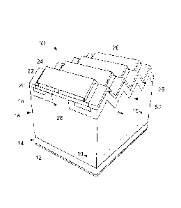
cellular structures (e.g., triangular, square, honeycomb, and so forth). For
example, FIG.
14 illustrates a top-down view of a hexagonal cellular design 210, which
includes an
example of MOSFET active areas 212 aligned with the illustrated SiC
crystallographic
axes 214 of a SiC substrate. During fabrication of the illustrated MOSFET
devices 212,
the hexagonal orientation of the SiC crystal structure (discussed above with
respect to
FIG. 7) may enable the simultaneous fabrication of identical trench features
(indicated by
the lines 216) that are each oriented in different directions (e.g., relative
to the axes 214)
and, at the same time, perpendicular to the channel periphery with trench
sidewalls lying
along specific crystallographic planes (e.g., a
(033-6) plane, a (11-i0 ) plane, or a (1-00 )
plane). It may be appreciated that the illustrated hexagonal cellular design
210 of FIG. 14
is axially symmetric and, accordingly, each of the trench features 216 will
provide the
same channel mobility. For example, in certain embodiments, the trench
features 216
may be trench features similar in structure to the trench features 56, 76, and
86 discussed
CA 02855325 2014-06-26
267455
above in FIGS. 3-6 and 10-13. By specific example, in certain embodiments, the
trench
features 216 may each be rectangular trench features (e.g., similar to trench
features 76
illustrated in FIGS. 12 and 13) and may further be oriented or aligned along a
(Inc) )
plane 96 of a hexagonal SiC substrate (e.g., as illustrated in FIG. 7). As set
forth in detail
above, these trench features 216 may increase the surface area and channel
width of each
of the MOSFET devices 212 and, accordingly, provide higher inversion channel
mobility
and lower on-state resistance.
[0054] Technical effects of the present approach include reducing device
resistance in
semiconductor devices (e.g., MOSFETs, IGBTs, and other suitable semiconductor
devices). Present embodiments include non-planar semiconductor devices (e.g.,
SiC
devices) that provide increased surface area per device and increased channel
width (e.g.,
increased channel periphery), which enables the production of lower resistance
SiC
devices. The disclosed device embodiments provide an increased effective
surface area
per die area that, in addition to reducing channel resistance, may decrease
one or more
contact resistances by increasing contact area at interfaces in the SiC device
structure.
Further, this approach is also applicable to cellular SiC device designs, such
as
honeycomb structures, to improve channel conduction and/or reduce on-state
resistance.
[0055] While there have been described herein what are considered to be
preferred and
exemplary embodiments of the present invention, other modifications of these
embodiments falling within the scope of the invention described herein shall
be apparent
to those skilled in the art.
21