Note: Descriptions are shown in the official language in which they were submitted.
CA 02855913 2014-05-14
DESCRIPTION
SEMICONDUCTOR LASER EXCITATION SOLID-STATE LASER
TECHNICAL FIELD
[0001]
The present invention relates to solid-state lasers
that are excited by semiconductor lasers, and in
particular to a module structure of a semiconductor laser
excitation solid-state laser with a planar
waveguide-type solid-state laser element.
BACKGROUND ART
[0002]
Until now, solid-state lasers (SSL) are widely known
as lasers for obtaining high output power, which use
optical materials, such as YV04 and YAG, doped with rare
earth elements including neodymium. In recent years, a
semiconductor laser excitation solid-state laser using
as its excitation light source a semiconductor laser (LD)
has become the mainstream in order to achieve reduction
in size and high efficiency. Furthermore, in order to
obtain high output power, the semiconductor laser for
excitation uses in many cases a semiconductor laser array
(LD array) in which a plurality of semiconductor lasers
1
CA 02855913 2014-05-14
is arranged in a direction perpendicular to the optical
axis of the semiconductor laser.
[0003]
The semiconductor laser excitation solid-state laser
is not only used for machining applications, but also
used as a light source for a display, because visible
light can be obtained by halving the wavelength of the
solid-state laser through second harmonic generation
(SHG) using a nonlinear optical element.
[0004]
The semiconductor laser excitation solid-state laser
module comprises: an LD and a solid-state laser element;
a heat-sink for cooling these elements; and a sub-mount
for relieving linear expansion stress between the LD and
solid-state laser elements and the heat-sink. Moreover,
in order to couple laser light output from the LD element
with the solid-state laser element and control a
transverse mode when the solid-state laser oscillates,
a coupling lens being interposed between the LD element
and solid-state laser element is often provided. (See,
for example, Patent document 1.)
[0005]
On the other hand, a method has been proposed, in which
the solid-state laser element has a planar waveguide
structure and thereby a transverse mode in a thickness
2
CA 02855913 2014-05-14
direction of the waveguide, that is, a vertical
transverse mode is controlled, and a transverse mode in
a width direction of the waveguide, that is, a horizontal
transverse mode is controlled by a thermal lens effect
produced inside the solid-state laser element, thereby
eliminating the coupling lens, so as to realize a more
compact semiconductor laser excitation solid-state
laser module. (See, for example, Patent document 2.)
[0006]
Patent document 1 is an example in which control of
the transverse mode of the laser light is achieved by
the coupling lens without using the waveguide structure
for the solid-state laser element. Patent documents 2
and 3 are examples in which the solid-state laser element
is provided with the planar waveguide structure so as
to control the vertical transverse mode of the laser light,
and in addition the solid-state laser element is disposed
on the sub-mount provided with stripe irregularities,
whereby thermal distribution is created inside the
waveguide with the absorbed laser energy used as a heat
source, thereby controlling the horizontal transverse
mode of the laser light.
Prior art document
Patent document
3
CA 02855913 2015-12-23
[0007]
Patent document 1: Japanese Laid-Open Patent
Publication No. H11-177167
Patent document 2: International Publication No.
W02006/103767
Patent document 3: International Publication No.
W02009/116131
DISCLOSURE OF THE INVENTION
[0008]
However, when the solid-state laser element is
provided with a planar waveguide but not provided with
a coupling lens as in Patent document 2, if obtaining
sufficient coupling efficiency is intended, the
light-emitting point of the LD element and the waveguide
of the solid-state laser need high precision positioning.
In Patent document 2, the LD element and solid-state laser
element are constructed in advance as sub-modules in
which these elements each are separately mounted on a
sub-mount and a heat-sink. These sub-modules need to be
joined and fixed by gluing and the like after they are
positionally adjusted to each other, therefore causing
a problem in that parts and assembly processes would
increase in number.
4
CA 02855913 2015-12-23
[0009]
The present invention has been made in view of the
problem as described above, and aims at providing a
semiconductor laser excitation solid-state laser module
that enables the LD element and solid-state laser element
to be easily positioned to each other and a high coupling
efficiency to be obtained, without using the sub-module
structure, in a semiconductor laser excitation
solid-state laser constructed using a solid-state laser
element provided with a planar waveguide.
[0010]
A semiconductor laser excitation solid-state laser
according to an aspect of the present invention comprises:
a planar waveguide-type solid-state laser element in
which claddings with a refraction index different from
that of a plate-shaped solid-state laser medium are formed
on both surfaces of the solid-state laser medium, and which
is disposed on a solid-state laser substrate; an LD
array in which a light-emitting layer sandwiched between
cladding layers is formed on an LD substrate, and which
generates laser light for exciting the solid-state laser
medium from an end face thereof; and a sub-
mount
substrate on which joining layers of two different
thicknesses are formed by metal plating on the same plane;
5
CA 02855913 2015-12-23
wherein
the planar waveguide-type solid-state laser element is
joined to the sub-mount substrate on a surface on the opposite
side of a surface on which the solid-state laser substrate
is mounted such that the planar waveguide-type solid-state
laser element is sandwiched between the solid-state laser
substrate and the sub-mount substrate, via a joining layer
of one of the thicknesses out of the joining layers of the
two different thicknesses, and the LD array is joined to the
sub-mount substrate on a surface on the light-emitting layer
side, via another joining layer of the other thickness out
of the joining layers of the two different thicknesses.
[0011]
The positions of the light-emitting points of the LD array
coincide with the waveguide center of the planar
waveguide-type solid-state laser element when the LD array
and planar waveguide-type solid-state laser element are
mounted on the sub-mount substrate; therefore, a highly
efficient semiconductor laser excitation solid-state laser
can be provided using a simple structure, without adjusting
the height positions of the LD array and planar
waveguide-type solid-state laser element to each other.
BRIEF DESCRIPTION OF THE DRAWINGS
6
CA 02855913 2014-05-14
[0012]
FIG. 1 is a side cross-sectional view showing a
semiconductor laser excitation solid-state laser
according to Embodiment 1 of the present invention;
FIG. 2 is a top view showing the semiconductor laser
excitation solid-state laser according to Embodiment 1
of the present invention;
FIG. 3 is a view showing an example of a method of
forming joining layers on a sub-mount substrate according
to Embodiment 1 of the present invention;
FIG. 4 is a side cross-sectional view showing a
semiconductor laser excitation solid-state laser
according to Embodiment 2 of the present invention; and
FIG. 5 is a top view showing the semiconductor laser
excitation solid-state laser according to Embodiment 2
of the present invention.
EMBODIMENTS FOR CARRYING OUT THE INVENTION
[0013]
Embodiment 1.
FIG. 1 is a side cross-sectional view of a
semiconductor laser excitation solid-state laser module
100 according to Embodiment 1; FIG. 2 is a top view thereof.
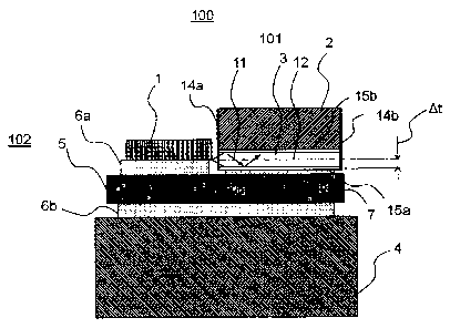
The semiconductor laser excitation solid-state laser
module 100 comprises: an LD array 1; a planar
7
CA 02855913 2014-05-14
waveguide-type solid-state laser element 101; a
sub-mount 102; and a heat-sink 4.
[0014]
The heat-sink 4 is made of a metallic material, such
as Cu, Fe or CuW, with high thermal conductivity. The
sub-mount 102 comprises: a sub-mount substrate 5 that
is made of an insulating material, such as AIN or SiC,
with high thermal conductivity; joining layers 6a and
6b that are disposed on the upper and lower surfaces of
this sub-mount substrate 5, respectively, and made of
a metallic material, such as Cu, Ni or Au, with high
thermal conductivity as well as high electrical
conductivity; and a stripe joining layer 7 that is
similarly made of a metallic material, such as Cu, Ni
or Au, with high thermal conductivity. This sub-mount
102 is mounted and fixed on the heat-sink 4 by a method
such as soldering. The LD array 1 is constructed with
an n-type cladding layer of a thickness of some 1 pm,
a light-emitting (active) layer of a thickness of some
0.01 pm, a p-type cladding layer of a thickness of some
1 pm and an electrode of a thickness of some 2 to 3 pm
formed on an LD substrate of a thickness of around 100
pm made of a material such as GaAs. This LD array 1 is
provided with a plurality of light-emitting points
arrayed in a width direction of an end face of a
8
CA 02855913 2014-05-14
plate-shaped solid-state laser medium 3 described later,
perpendicular to the optical axis of the solid-state
laser. In addition, the LD array 1 is electrically and
mechanically joined to the joining layer 6a of the
sub-mount 102, by a method such as soldering, on the
surface on the opposite side of the LD substrate, that
is, on the surface on the light-emitting layer side (with
so-called junction down) .
[0015]
The planar waveguide-type solid-state laser element
101 comprises: the plate-shaped solid-state laser medium
3 made of a material, such as YV04 or YAG, doped with
rare-earth elements including neodymium; claddings 15a
and 15b that are made of a material with a refraction
index different from that of the solid-state laser medium
3 and disposed on both upper and lower surfaces of the
plate-shaped solid-state laser medium 3, respectively;
and a solid-state laser substrate 2 that holds the
solid-state laser medium 3 and claddings 15a and 15b.
The solid-state laser medium 3 on both upper and lower
surfaces of which are disposed the claddings 15a and 15b
forms the planar waveguide. On the end face of the planar
waveguide-type solid-state laser element 101 on the LD
side is disposed a reflective coating 14a that passes
the wavelength of excitation laser light from the LD and
9
CA 02855913 2014-05-14
reflects the wavelength of solid-state laser light that
is emitted by stimulated emission from the solid-state
laser medium 3, and on the end face on the output side
thereof is disposed a reflective coating 14b that
partially reflects the solid-state laser light. The
planar waveguide-type solid-state laser element 101 is
mechanically joined, by a method such as soldering, to
the stripe joining layer 7 of the sub-mount 102 with the
solid-state laser medium 3 facing downward.
[0016]
Additionally, a thickness difference of At is
provided between the two joining layers of the sub-mount
102: the joining layer 6a on which the LD array 1 is
mounted; and the stripe joining layer 7 on which the
planar waveguide-type solid-state laser element 101 is
mounted. Since the LD array 1 is disposed with the
junction down here, the height of the light-emitting
layer of the LD array 1 from its bottom surface is given
by the following equation:
[Height of light-emitting layer him] = [electrode
thickness hmetal] [p-type cladding thickness hperad]
[0017]
Moreover, since the planar waveguide-type
CA 02855913 2014-05-14
solid-state laser element 101 is disposed with the
solid-state laser medium 3 facing downward, the height
of the waveguide center 12 from the bottom surface of
the planar waveguide-type solid-state laser element 101
is expressed as follows:
[Height of waveguide center hcenter] = [thickness of
solid-state laser medium hcore] /2
[cladding thickness
hcrad] .
[0018]
The thickriess At between the joining layer
6a and stripe joining layer 7 is made as given by the
following equation:
[At] = [height of waveguide center hcenter1 - [height of
light-emitting layer hm3].
[0019]
As described above, since the electrode thickness
hmetai. is 2 to 3 pm, the p-type cladding layer thickness
hperad some 1 pm, and the thickness of the solid-state
laser medium 3 typically some 40 pm, At becomes some 20
pm. When each layer is formed by plating, a difference
in thickness such as this can be provided between the
11
CA 02855913 2014-05-14
joining layer 6a and stripe joining layer 7 by adjusting
the plating time. Furthermore, the ID array 1 and planar
waveguide-type solid-state laser element 101 are joined
by soldering and the like to the joining layer 6a and
stripe joining layer 7 of the sub-mount 102,
respectively; however, the thickness of the solder layers
is a few pm, so the thicknesses of each solder layer can
easily be made nearly the same.
[0020]
The operation will be explained next using FIG. 1 and
FIG. 2. When the LD array 1 is made to oscillate and emit
light, excitation laser light 11 propagates with a
certain diverging angle in a vertical and a horizontal
direction and is incident on the solid-state laser medium
3 of the planar waveguide-type solid-state laser element
101. Light components of the incident excitation laser
light 11 that cause total reflections at the claddings
15a and 15b control the thickness-direction mode of the
waveguide, and are absorbed in the solid-state laser
medium 3, while coupling and propagating inside the
planar waveguide. Moreover, part of the absorbed energy
is converted into heat. The heat generated inside the
solid-state laser medium 3 is dissipated through the
stripe joining layer 7. Here, the stripe joining layer
7 includes a plurality of stripe joining layers extending
12
CA 02855913 2014-05-14
in an optical axis direction of the solid-state laser
as shown in FIG. 2. Cooling paths are short at portions
where the cladding 15a on the surface of the solid-state
laser medium 3 contacts the stripe joining layer 7,
whereas the paths are long at portions where it doesn't.
Therefore, there rises temperature distribution in the
solid-state laser medium 3, in which temperatures at
central portions corresponding to the portions that do
not contact the stripe joining layer 7 become relatively
high. This temperature distribution causes distribution
of the refraction index of the material, that is, the
so-called thermal lens effect, and thereby the same
effect as providing focal lenses at each portion of the
solid-state laser medium contacting the stripe joining
layer 7 can be produced.
[0021]
Furthermore, the solid-state laser medium 3 causes
stimulated emission as excited by the absorbed excitation
light; using the reflective coatings 14a and 14b as a
resonator, the vertical transverse mode is controlled
by the waveguide and the horizontal transverse mode is
controlled by the thermal lens effect, thereby laser
oscillation taking place.
[0022]
If the positions of the light-emitting points of the
13
CA 02855913 2014-05-14
LD array 1 are deviated from the vertical position of
the solid-state laser medium 3 here, the laser light is
not sufficiently coupled with the waveguide, thereby
leading to deterioration of efficiency. However, in the
semiconductor laser excitation solid-state laser module
according to this Embodiment 1, the light-emitting points
of the LD array 1 are arranged to coincide with the
waveguide center in advance by making the difference in
thickness between the stripe joining layer 7 and joining
layer 6a At, so that the excitation light can be highly
efficiently coupled with the waveguide without adjusting
the height positions of the light-emitting points of the
LD array 1 and that of the planar waveguide-type
solid-state laser element 101.
[0023]
Next, a process will be explained in which the
sub-mount substrate 5 is mechanically fixed to the
heat-sink 4 by soldering and the LD array 1 and planar
waveguide-type solid-state laser element 101 to the
sub-mount 102. In this case, heating and cooling
processes for melting solder become necessary.
[0024]
A case using AuSn as the solder will be described
In the heating process for melting the AuSn solder, the
heat-sink 4, the sub-mount 102, the LD array 1 and the
14
CA 02855913 2014-05-14
planar waveguide-type solid-state laser element 101
thermally expand as their temperatures rise up, depending
on the linear expansion coefficient of each of the
materials. In addition, in the cooling process for
solidifying the AuSn solder, thermal contraction takes
place in each of the components as their temperatures
drop. The LD array 1 and planar waveguide -type
solid-state laser element 101 are mechanically joined
to the sub-mount 102 when their temperatures reach 2800C,
which is the melting point of the AuSn solder; however,
in the cooling process from the melting point to room
temperature, if there is any difference between the
thermal contraction of the sub-mount 102 and that of the
LD array 1 and planar waveguide-type solid-state laser
element 101, stress is imposed on the interior of the
LD array 1 and that of the planar waveguide - type
solid-state laser element 101. Furthermore, the greater
the difference in the foregoing thermal contraction, the
greater the stress imposed thereon, which would shorten
the driving lifetime of the planar waveguide -type
solid-state laser.
[0025]
When a material for the LD array 1 is GaAs and materials
for the solid-state laser medium 3 and solid-state laser
substrate 2 are YV04, their respective linear expansion
CA 02855913 2014-05-14
coefficients are 6.6 x 10⁻⁶ mm/mm and 1.7 x 10⁻⁶ mm/mm.
While on the other hand, when a material for the sub-mount
substrate 5 is SiC, the linear expansion coefficient of
SiC is 3.7 x 10⁻⁶ mm/mm, which is close enough to those
of the materials for the LD array 1, solid-state laser
medium 3 and solid-state laser substrate 2; therefore,
stress caused in the LD array 1 and planar waveguide-type
solid-state laser element 101 can be made small enough,
when the LD array 1 and planar waveguide-type solid-state
laser element 101 are soldered and even when the
temperature of the semiconductor laser excitation
solid-state laser module 100 rises up in its driving
operation. Moreover, AIN and Si, which are low-expansion
insulation materials other than that, may be used for
the sub-mount substrate material.
[0026]
Next, as an example of a method of forming the joining
layers 6a, 6b and 7 on the sub-mount substrate 5, a method
of forming each layer by metal plating will be explained
using FIG. 3. First, a resist layer 21a corresponding
to the joining layers 6a and 6b is formed on the sub-mount
substrate 5 (see FIG. 3 (a) ) ; plating of a thickness of
tl is performed by adjusting the plating time (see FIG.
3 (b) ) . Secondly, the resist layer 21a is removed (see
FIG. 3 (c) ) , and then a resist layer 21b corresponding
16
CA 02855913 2014-05-14
to the stripe joining layer 7 is formed anew (see FIG.
3 (d)). At this moment, the resist layer 21b is formed
so as to also cover the already-formed joining layers
6a and 6b. Thirdly, plating of a thickness of t2 is
performed by adjusting the plating time (see FIG. 3 (e)),
and following that the resist layer 21b is removed (see
FIG. 3 (f)), whereby the joining layers 6a and 6b of the
thickness tl and stripe joining layer 7 of the thickness
t2 are formed. By making tl - t2 At here, the
light-emitting part of the LD array 1 and the incident
center of the solid-state laser medium 3 can be aligned
with each other, so that a highly efficient semiconductor
laser excitation solid-state laser can be provided
without adjusting their positions. Additionally, even
if an error of this thickness difference At is some 10
pm when the thickness of the solid-state laser medium
is, for example, 40 pm, excitation efficiency will not
be deteriorated so much. It is easy to adjust the plating
thickness within an error such as this. Additionally,
an allowable error differs depending on, for example,
the thickness of the solid-state laser medium 3, the
diverging angle of laser light the LD array 1 generates,
the distance between the end face of the solid-state laser
medium 3 and the light-emitting points of the LD array
1, and so forth; however, it is decided to be a value
17
CA 02855913 2014-05-14
at which the excitation efficiency is reduced by 10 %,
for example, or more preferably by 5 t, from the maximum
efficiency. That is to say, taking into consideration
deterioration rates of efficiency in individual planar
waveguide- type semiconductor laser excitation
solid-state lasers, a predetermined error is decided for
each.
[0027]
As described above, the difference in thickness
between the joining layers of two different thicknesses
has only to be set to become the dimensions of the
difference in height between the planar waveguide center
from the plane on which the planar waveguide -type
solid-state laser element is joined to the joining layer
and the light-emitting layer of the LD array from the
outer surface thereof on the light-emitting layer side
and an error that is not greater than a predetermined
error.
Additionally, the joining layers 6a and 6b and stripe
joining layer 7 each may be a plating layer with a
laminated structure in which plating layers of a
plurality of different metals are formed in sequence.
Furthermore, these joining layers are not plating layers
but the joining layer 6a and stripe joining layer 7 may
be formed by joining to the sub-mount substrate 5 metal
18
CA 02855913 2014-05-14
sheets whose thicknesses are different_ by At from each
other.
[0028]
As described above, the semiconductor laser
excitation solid-state laser according to Embodiment 1
of the present invention is constructed in such a way
that. the LD array 1 and planar waveguide-type solid-state
laser element 101 are joined to the common sub-mount
substrate 5, via the joining layer 6a and stripe joining
layer 7, respectively, and the thickness difference At
is provided between the joining layer 6a and stripe
joining layer 7; therefore, the light-emitting part of
the LD array 1 and the incident center of the solid-state
laser medium 3 can be aligned with each other without
adjusting their positions, so that a highly efficient
semiconductor laser excitation solid-state laser can be
provided.
[0029]
Embodiment 2
FIG. 4 is a side cross-sectional view of a
semiconductor laser excitation solid-state laser module
100 according to Embodiment 2; FIG. 5 is a top view thereof.
In FIG. 4 and FIG. 5, the same reference numerals as those
in FIG. 1 and FIG. 2 represent the same or corresponding
19
CA 02855913 2014-05-14
parts In. this Embodiment 2, the joining layer for joining
the planar waveguide-type solid-state laser element 101
to the sub-mount 5 is made to be an unbroken joining layer
70 similar to the joining layer 6a, as shown in the top
view of FIG. 5.
[0030]
A case of a semiconductor laser excitation
solid-state laser system has been explained in Embodiment
1, in which the horizontal transverse mode is controlled
with the planar waveguide-type solid-state laser element
mounted on the stripe joining layer 7. However, the same
effect as that in Embodiment 1 can be produced even if
this invention is applied to other semiconductor laser
excitation solid-state laser systems, such as one in
which the excitation light from the ID array is coupled
with the planar waveguide-type solid-state laser element
101 through, for example, a micro lens array so as to
control the horizontal transverse mode.
[0031]
That is to say, the same as Embodiment 1, the
difference in thickness between the joining layer 70 and
joining layer 6a is made At in this Embodiment 2 as well,
whereby the light-emitting part of the LD array 1 and
the incident center of the solid-state laser medium 3
are aligned with each other without adjusting their
CA 02855913 2014-05-14
positions, so that a highly efficient semiconductor laser
excitation solid-state laser can be provided.
DESCRIPTION OF THE REFERENCE NUMERALS
[0032]
1: LD array
2: solid-state laser substrate
3: solid-state laser medium
4: heat-sink
5: sub-mount substrate
6a, 6b, 70: joining layer
7: stripe joining layer
15a, 15b: cladding
101: planar waveguide-type solid-state laser element
102: sub-mount
21