Note: Descriptions are shown in the official language in which they were submitted.
CA 02856643 2014-05-22
WO 2013/053683 PCT/EP2012/069928
- 1 -
A Spectrometer
Field of the Invention
The present invention relates to a spectrometer. More particularly, but not
exclusively, the present invention relates to a spectrometer comprising a
waveguide
including an elongate part and an input for guiding light to the elongate
part.
Background of the Invention
Spectrometers are used in many applications for measuring properties of light
across a range of wavelengths. For example, a spectrometer can be used for
compositional analysis, by obtaining absorption or emission spectra for an
object of
interest. The presence and location of peaks within the spectra can indicate
the
presence of particular elements or compounds. Spectrometers are commonly used
for analysis at optical wavelengths, but can also be used at other wavelengths
such
as microwave and radio wavelengths.
Spectrometers are typically relatively complex and expensive devices that
require the
alignment of a number of moving parts to be controlled with high precision.
For
example, a typical spectrometer may focus light onto a diffraction grating to
split an
incident beam into separate wavelengths, and the diffraction grating may be
rotated
to a specific angle to direct light of a particular wavelength towards a
detector. In
recent years chip-based spectrometers have been developed which can be highly
miniaturised, have no moving parts, and can be manufactured using well-
established
lithography techniques. An example of such a spectrometer-on-a-chip is shown
in
Fig. 1.
The chip spectrometer 100 comprises a substrate 110, onto which are patterned
a
waveguide 120 and a plurality of disk resonators coupled to the waveguide. The
waveguide 120 guides the input light to the disk resonators. Light is input to
one
end of the waveguide, and each resonator 130 is arranged to support a resonant
mode at a particular wavelength such that only light of that wavelength is
coupled
into the resonator 130. On top of each disk resonator 130 is an electrode 140
for
detecting current that is proportional to the amount of light present in that
CA 02856643 2014-05-22
WO 2013/053683 PCT/EP2012/069928
- 2 -
resonator. The current detected in each resonator therefore indicates the
amount of
light at that wavelength that was present in the input beam of light. Each
electrode
140 is further connected to a signal bond pad 150 for connecting the
spectrometer
100 to an external device for measuring the current. The light input to the
waveguide 120 has to be closely aligned to the centre of the waveguide 220, in
order
to achieve optimum coupling into the waveguide 220.
Summary of the Invention
According to the present invention, there is provided a spectrometer
comprising a
substrate and a waveguide on the substrate, the waveguide comprising an
elongate
part and a tapered input for guiding electromagnetic radiation to the elongate
part,
wherein the tapered input has an input end for receiving the electromagnetic
radiation and an output end coupled to the elongate part, the width of the
input end
being greater than the width of the output end.
The width of the input end may be greater than a free-space wavelength kf of
the
electromagnetic radiation which the waveguide is arranged to receive.
The width of the input end may be between 1.5XT and 5XT, where kf is the free-
space
wavelength.
The tapered input may have a length designed to allow the optical mode to
adiabatically compress into the waveguide.
The elongate part may have substantially the same width as the width of the
output
end of the tapered input.
The width of the elongate part may be substantially the same as the wavelength
kw
of the radiation in a material from which the waveguide is formed.
The elongate part and the tapered input may be formed from the same material.
The elongate part and the tapered input may be integrally formed.
CA 02856643 2014-05-22
WO 2013/053683 PCT/EP2012/069928
- 3 -
The radiation which the waveguide is arranged to guide may comprise a
plurality of
wavelengths and the spectrometer may further comprise a plurality of
resonators
coupled to the elongate part of the waveguide, each resonator being configured
to
support a resonant mode at one of the plurality of wavelengths.
Brief Description of the Drawings
Embodiments of the present invention will now be described, by way of example
only, with reference to Figures 2 to 6 of the accompanying drawings, in which:
Figure 1 illustrates a prior art spectrometer-on-a-chip;
Figure 2 illustrates a spectrometer having a tapered input to a waveguide,
according
to an embodiment of the present invention;
Figure 3 illustrates a tapered input to a waveguide, according to an
embodiment of
the present invention;
Figure 4 illustrates a finite-difference time-domain (FDTD) simulation of a
light
beam input off-centre to the tapered input of Fig. 3;
Figure 5 is a graph showing coupling of light into a tapered waveguide having
a 3p,m
wide input; and
Figure 6 is a graph showing coupling of light into a tapered waveguide having
a 5p,m
wide input.
Detailed Description
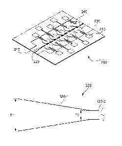
Referring now to Fig. 2, a spectrometer having a tapered input to a waveguide
is
illustrated, according to an embodiment of the present invention. As shown in
Fig.
2 the spectrometer 200 is a spectrometer-on-a-chip, comprising a substrate
210,
elongate waveguide 220 and a plurality of disk resonators 230 coupled to the
waveguide. The waveguide may be a ridge waveguide. Each disk resonator 230 is
provided with an electrode 240 for sensing a current in the disk resonator,
the
electrode 240 being connected to a bond pad 250 for connecting the
spectrometer
200 to other components. The drawings are schematic, and provided for
illustrative
purposes only. In particular, other layers and components may be present even
though for clarity they are omitted in Fig. 2. For instance, additional layers
may be
present in the waveguide 220 and/or the disk resonators 230.
CA 02856643 2014-05-22
WO 2013/053683 PCT/EP2012/069928
- 4 -
Like the conventional chip-based spectrometer of Fig. 1, in the present
embodiment
the elongate waveguide 220 is coupled to the disk resonators 230 to guide
input
light to the disk resonators 230. Each disk resonator 230 is configured to
support a
resonant mode at a particular predetermined wavelength of light, such that
only
light of the predetermined wavelength is coupled from the waveguide 220 into
the
disk resonator 230. However, unlike a conventional spectrometer in which the
elongate waveguide has a uniform width along its length, in the present
embodiment
the waveguide includes a tapered input coupled to the elongate part. The
tapered
input can ensure that even when the input light beam is not perfectly aligned
with
the centre line of the waveguide, a substantial proportion of the input energy
can
still be coupled into the elongate portion and directed to the disk
resonators.
Therefore, the use of a tapered input can allow manufacturing tolerances to be
reduced, by relaxing the requirement for the chip-based spectrometer to be
precisely
aligned to the source of the input light beam.
A waveguide having a tapered input similar to the one shown in Fig. 2 is
illustrated
in more detail in Fig. 3. In Figs. 2 and 3, the degree of taper is exaggerated
for
clarity, i.e. the horizontal and vertical scales in Fig. 3 are not the same.
As shown in
Fig. 3, the waveguide 320 includes a tapered input 320-1 and an elongate part
320-2.
The width of the elongate part 320-2 may be substantially similar to the width
of the
elongate waveguide of the conventional spectrometer in Fig. I. The width of
the
elongate part may be designed to support a single mode of resonance. For
example,
the width of the elongate part 320-2 may be similar to or slightly larger than
one
wavelength kw of the input light beam in the waveguide 320. However, it is
contemplated that other widths are possible.
Also, as shown in Fig. 3, the tapered input has an input end with a width of
T1, and
an output end with a width of T2. The output end is coupled to the elongate
part
320-2, such that light input to the tapered input 320-1 is guided towards, and
coupled into, the elongate part 320-2. The width of T1 is substantially
greater than
the width T2 of the output end. In some embodiments, the width of T1 is also
greater than the free-space wavelength kf of the radiation that is received by
the
CA 02856643 2014-05-22
WO 2013/053683 PCT/EP2012/069928
- 5 -
waveguide. The input beam may include a plurality of wavelengths, for example
when the device is a spectrometer as shown in Fig. 2. In such cases, the
wavelengths kf and kw may, for example, be the mean wavelengths of the
wavelength
range of interest of the input beam in free-space and in the material of the
waveguide respectively. The length of the tapered input 320-1 may be designed
in
conjunction with the width of the tapered input to ensure that the resonance
mode
compresses adiabatically.
In the present embodiment, the output end of the tapered input 320-1 is
directly
connected to the elongate part 320-2 to couple light into the elongate part
320-2.
In particular, in the present embodiment the tapered input 320-1 and the
elongate
part 320-2 are integrally formed as a single component, and are formed of the
same
material, specifically InP and alloys thereof. However, in other embodiments
other
arrangements are possible, for example the tapered input 320-1 and elongate
part
320-2 could be separated by a small air gap, and/or could be formed of
different
materials.
The waveguide 120 may also be integrally formed with the resonators 130. It
may be
formed on the substrate 110 in the same processing step as the resonators and
from
the same material, such as a suitable semiconductor material. The substrate
may be
manufactured from any suitable type of semiconductor. For example, the
substrate
may be formed from n-doped InP with a dopant concentration of about 1-3x
1018cm 3.
On top of the substrate there may be provided an etch-stop layer, which
prevents etching of the substrate, and on top of the etch-stop layer there may
be
provided a support layer. As an example, an etch-stop layer may be formed from
n-
doped InGaAsP with a dopant concentration of 0.18-1.2x 1018cm 3 and the
support
layer may be formed from n-doped InP with a dopant concentration of 4-6x1017cm
3. The waveguide and the resonators are then provided as one or more layers on
top
of the support layer. The layers may be formed from undoped InGaAsP. On top of
the one or more layers forming the waveguide there may be formed a capping
layer.
The capping layer may be formed from p-doped InP with a dopant concentration
of
about 2x1018cm 3. There may also be provided an isolation layer for
metallisation on
top of the capping layer.
CA 02856643 2014-05-22
WO 2013/053683 PCT/EP2012/069928
- 6 -
The one or more layers that provide the waveguide and the resonators may have
a
higher refractive index than the support layer and the capping layer and the
waveguide is formed from the refractive index contrast between the layers
forming
the waveguide and the support layer and capping layers. It will be appreciated
that
the layer structure described above is just an example and one or more layers
may
be removed or replaced. For example the structure may not comprise a support
layer, in which case the waveguide is provided between the refractive index
contrast
between the waveguide layers and the capping layer and the substrate.
The one or more layers that provide the waveguide and the resonators may
comprise an absorbing layer with a band gap designed to absorb the radiation.
It
may be designed to have a low absorption coefficient to limit the absorption
in the
waveguide. The one or more layers may form an active layer stack comprising
two
cladding layers between which an active absorbing layer is sandwiched. The
band
gap of the absorbing layer may be less than the lowest-energy photon of
interest, i.e.
lower than the energy of a photon of the longest wavelength that the
spectrometer
is configured to detect. In this way, the composition of the absorbing layer
can be
used in all disk resonators in the spectrometer. The capping layer, the
support layer
and the cladding layers may have band gaps that are greater than the highest-
energy
photon of interest. The absorbing layer may be a quantum well. The quantum
well
may be grown by molecular beam epitaxy or chemical vapour deposition which can
control the layer thickness down to monolayers. The quantum well is
sufficiently
thin to have little or no influence on the optical field in the waveguide. For
example
the quantum well may have a thickness of approximately 3nm. When light of a
particular wavelength enters the resonator from the waveguide, it travels
multiple
cycles around the resonator and the photons can be absorbed by the material in
the
quantum well as the band gap is sufficiently low for even the lowest-energy
photons
to excite electrons from the valence band into the conduction band, generating
electron-hole pairs. The resulting current can be measured, and is
proportional to
the amount of light energy in the disk resonator. The waveguide ensures that
the
optical field is at a maximum over the quantum well which helps to increase
absorption.
CA 02856643 2014-05-22
WO 2013/053683 PCT/EP2012/069928
- 7 -
However, it will be appreciated that the structure does not have to be uniform
across the resonators and the waveguide. The absorbing layer may not be
provided
in the waveguide. The absorbing layer in the waveguide 120 can be selectively
etched and replaced by a wider band-gap alloy or the absorbing layer can to
only be
deposited in the disk resonators 130 in the first place.
It should of course be realised that the present invention is not limited to
the layer
structure described above, and in other embodiments other structures may be
used.
Referring now to Fig. 4, a finite-difference time-domain (FDTD) simulation is
illustrated of a light beam being input off-centre to the tapered waveguide
shown in
Fig. 3. Specifically, in Fig. 4 the input light beam has a free-space center
wavelength
of 1600 nm, and is input at an offset of 0.5 p.m from the centre axis of the
waveguide. If the waveguide is formed from a material with, for example, a
refractive index of 3.1, the radiation in the waveguide material may have a
wavelength of just over 500nm. In the present embodiment the width T1 of the
input end of the tapered input 320-1 is 3 p.m, the width T2 of the output end
coupled to the waveguide 320-2 is 0.75 p.m, and the length of the tapered
input 320-
1 is about 42 m. Accordingly, the width T1 of the input end is considerably
larger
than the free-space wavelength kf of the radiation. However, it should be
realised
that the present invention is not limited to the above dimensions. As shown in
Fig.
4, even when light is input off-centre to the waveguide, i.e. not aligned with
the
central axis of the waveguide, a substantial proportion of the input energy is
still
coupled into the tapered input 320-1 having a larger width at the input end,
and is
guided by the taper into the narrower elongate part 320-2. It was shown that
about
80% of the power was collected and 40% of the power was propagated to a
detector
located 50 p.m from the entrance to the waveguide in the elongate part.
In contrast to the embodiment shown in Figs. 3 and 4, if a light beam is input
at an
offset of 0.5 p.m to a 0.75 p.m wide non-tapered waveguide such as the one
shown in
Fig. 1 but otherwise of a similar construction, only 10 % of the input power
is
coupled into the waveguide and only 5% of the power is propagated to a
detector
CA 02856643 2014-05-22
WO 2013/053683 PCT/EP2012/069928
- 8 -
located 50 p.m from the entrance to the waveguide. The use of a tapered input,
as
shown in Figs. 3 and 4, therefore allows substantially more input energy to be
coupled into the waveguide, particularly when an input beam is improperly
aligned
with the centre axis of the waveguide.
Referring now to Figs. 5 and 6, graphs are illustrated to show coupling of
input light
of wavelength 1.6 p.m into the elongate part of a waveguide similar to that of
Figs.
2, 3 and 4, for different widths of the input end of the tapered input. The
graphs
show the results of simulations in which a monitor value corresponding to a
proportion of input energy is plotted against distance into the waveguide. In
both
Figs. 5 and 6, the input beam is aligned on-axis with the waveguide, i.e. is
not offset
from the waveguide axis. The graph in Fig. 5 shows results for an input end
width
of 3 p.m, and the graph in Fig. 6 shows results for an input end width of 5
m. In
both cases, the output end of the tapered input and the elongate part is
designed to
support a single mode.
As shown in Fig. 5, for an input end width of 3 m substantially all the input
light
energy is coupled into the waveguide at points close to the waveguide axis,
shown
by the solid and dotted lines in Fig. 5. The dashed line shows the amount of
energy
coupled into the waveguide at a certain distance from the waveguide axis, and
shows
that in this case about 45 '1/4 of the input energy is still coupled into the
waveguide.
Also, as shown in Fig. 6, for an input end width of 5 m about 95 % of input
light
energy is coupled into the waveguide at points close to the waveguide axis,
shown
by the solid and dotted lines. The dashed line shows that about 35 '1/4 of
input
energy is coupled into the waveguide at a distance from the waveguide axis.
That is,
if the taper width is increased beyond a certain point, the amount of input
energy
coupled into the elongate part of the waveguide begins to be reduced.
Therefore
preferably the taper width may be chosen from within a certain range, for
example
between 1.52 and 52, where X, is the free space wavelength. In some
embodiments,
the taper width may be chosen from within a range of 1.5 X, and 2.5 X,.
However, the
exact values depend on the materials forming the waveguide. As mentioned
before,
a suitable material for the waveguide may be a semiconductor material
CA 02856643 2014-05-22
WO 2013/053683 PCT/EP2012/069928
- 9 -
Although embodiments of the present invention have been described in which a
waveguide has an input that is tapered symmetrically in the horizontal plane,
i.e. a
plane parallel to the surface of the substrate, the present invention is not
limited to
this arrangement. For example, in some embodiments the tapered input of the
waveguide may be asymmetric. Also, the tapered input may be tapered in the
vertical direction, instead of or as well as being tapered in the horizontal
direction.
In some embodiments, the tapered input may be conical, or may be shaped as a
conical section. Furthermore, although in the described embodiment a tapered
input has an output end with the same width as the elongate part to which it
is
coupled, in other embodiments the width of the output end may be greater or
less
than the width of the elongate part, for example the waveguide may have a
stepped
profile where the output end is coupled to the elongate part.
Additionally, although embodiments have been described for receiving and
guiding
electromagnetic radiation at optical wavelengths, the present invention is not
limited
to optical wavelengths. For example, a tapered waveguide may be configured to
guide electromagnetic radiation of any wavelength, for example electromagnetic
radiation at a microwave wavelength instead of an optical wavelength.
Whilst certain embodiments of the present invention have been described above,
the skilled person will understand that many variations and modifications are
possible without departing from the scope of the invention as defined in the
accompanying claims.
It will be appreciated that the spectrometer, with respect to which the
invention has
been described, may be considered to be, or form part of, a spectrophotometer.
Therefore, where the term "spectrometer" has been used, the term could have
been
replaced with the term "spectrophotometer".
Additionally, although the spectrometer has been described to comprise disk
resonators, the described waveguide may be used to guide light into any type
of
CA 02856643 2014-05-22
WO 2013/053683
PCT/EP2012/069928
- 10 -
resonators. For example, the resonators may be any high Q cavities, such as
spherical resonators, microrings etc.