Note: Descriptions are shown in the official language in which they were submitted.
CA 02857093 2015-03-13
ULTRASONIC SENSOR MICROARRAY AND METHOD OF
MANUFACTURING SAME
SCOPE OF THE INVENTION
The present invention relates to a micromechanical system (MEMS) and its
method of
manufacture, and more particularly three-dimensional MEMS devices such as
sensor
microarrays which may function as part of a capacitive micromachined
ultrasonic transducer
(CMUT). In a preferred application, the present invention relates to an
ultrasonic sensor
microarray and its method of manufacture which incorporates or simulates a
hyperbolic
paraboloid shaped sensor configuration or chip, and which incorporates
benzocyclobutene
(BCB) as a structural component. Suitable uses for the CMUT include non-
vehicular and/or
vehicle or automotive sensor applications, as for example in the monitoring of
vehicle blind-
spots, obstructions and/or in autonomous vehicle drive and/or parking
applications.
BACKGROUND OF THE INVENTION
In the publication Design of a MEMS Discretized Hyperbolic Paraboloid Geometry
Ultrasonic Sensor Microarray, IEEE Transactions On Ultrasonics,
Ferroelectrics, And
Frequency Control, Vol. 55, No. 6, June 2008, the inventor describes a concept
of a discretized
hyperbolic paraboloid geometry beam forming array of capacitive micromachined
ultrasonic
transducers (CMUT) which is assembled on a microfabricated tiered geometry.
1
CA 02857093 2015-03-13
In initial fabrication concepts, for CMUTs, Silicon-on-Insulator (SOT) wafers
were
subjected to initial cleaning, after which a 10 nm seed layer of chromium is
then deposited
thereon using RF-magnetron sputtering to provide an adhesion layer. Following
the deposition
of the chromium adhesion layer, a 200 nm thick gold layer is deposited using
conventional
CMUT deposition processes. After gold layer deposition, a thin layer of AZ4620
photoresist is
spin-deposited on the gold layer, patterned and etched. The gold layer is then
etched by
submerging the wafer in a potassium iodine solution, followed by etching of
the chromium
seed layer in a dilute aqua regia, and thereafter rinsing. The device layer is
thereafter etched
further to provide acoustical ports for static pressure equalization within
the diaphragm, and
allowing for Si02 removal during a release stage.
A top SOI wafer is etched using a Bosch process deep reactive ion etch (DRIE)
in an
inductively coupled plasma reactive ion etcher (ICP-RIE). After metal etching
with the Bosch
and DRIE etch, the remaining photoresist is removed by 02 ashing processing.
Bosch etched
wafer is submerged in a buffer oxide etch (BOE) solution to selectively etch
Si02 without
significantly etching single crystal silicon to release the selective
diaphragms. Following
etching and rinsing, the sensing surfaces (dyes) for each of the arrays are
assembled in a
system-on-chip fabrication and bonded using conductive adhesive epoxy.
The applicant has appreciated however, existing processes for the fabrication
of
capacitive micromachined ultrasonic transducers require precise manufacturing
tolerances.
As a result, the production of arrays of CMUT sensors or transducers on a
commercial scale
has yet to receive widespread penetration in the marketplace.
United States Patent No. 6942750 to Chou et al., describes a construct and
process of patterned wafer bonding using photosensitive benzocyclobutene (BCB)
in
the fabrication of a 3D MEMS construction. In particular, Chou et al discloses
the
use of a light activated photosensitive BCB as an assembly adhesive used to
effect
precision patterning wafer bonding, with the resulting three-
2
CA 02857093 2014-05-27
WO 2014/066991
PCT/CA2013/000937
dimensional MEMS microstructure achieved with BCB adhesive layers adding to
the Z-
height of the assembled wafer complex.
SUMMARY OF THE INVENTION
The inventor has appreciated a new and/or more reliable CMUT array design may
be
achieved by improved manufacturing methods and/or with adjustable operating
frequencies.
One non-limiting object of the present invention is to provide an ultrasonic
sensor which
incorporates one or more CMUT microarrays or modules for transmission of and
receiving
signals, and which may be more immune to one or more of a variety of different
types of
ultrasound background noise sources, such as road noise, pedestrian, cyclist
and/or animal
traffic, car crash sounds, industrial works, power generation sources and the
like.
In one construction, the present invention provides a three-dimensional MEMS
device,
and more preferably a CMUT transducer, which incorporates a silicon wafer
construct which
incorporates benzocyclobutene (BCB) as a structural component in the Z-axis.
Another non-limiting construction provides an ultrasonic CMUT based microarray
which provides programmable bandwidth control, and which allows for CMUT
microarray
design to be more easily modified for a variety of different sensor
applications.
A further non-limiting construction provides an ultrasonic sensor which
incorporates a
transducer microarray module or sub-assembly which has a substantially
flattened curvature,
preferably which has a curvature less than +Ur, and more preferably less than
about 10, and
which in operation simulates a hyperbolic paraboloid shaped chip array
geometry.
One embodiment of the invention provides a capacitive micromachined ultrasonic
transducer (CMUT) based microarray module which incorporates a number of
transducers.
The microarray module is suitable for use in vehicle, as well as non-vehicle
rail, aircraft and
other sensor applications. For example the module may be provided as part of a
hand or body
position sensor, as well as in warning and/or control systems for monitoring
blind-spots,
3
CA 02857093 2014-05-27
WO 2014/066991 PCT/CA2013/000937
adjacent obstructions and hazards, and/or in vehicle road position warning
and/or autonomous
drive applications.
Another embodiment of the invention provides a method for the manufacture of a
CMUT based microarray of transducer/sensors, and more preferably CMUT based
microarray
modules, which are operable to emit signals over a number and/or range of
frequencies, and
which may be arranged to minimize frequency interference from adjacent
sensors. In one
possible preferred method of manufacture, conventional (i.e. non-
photosensitive)
benzocyclobutene (BCB) is used as an adhesive layer in the formation of a
microarray as wafer
construct.
It is envisioned that the invention and provide a simplified and reliable
method of
manufacturing CMUT microarray modules, further an ultrasonic sensor
manufacturing process
in which multiple CMUT microarrays modules may be more easily provided either
in a
hyperboloid parabolic geometry using a molding, stamping or three dimensional
(3D) printing
process; or which simulates such a configuration. Further, by changing the
orientation of the
individual CMUT microarray modules in the sensor array, it is possible to
select preferred
output beam shapes.
In another possible embodiment, the present invention provides a sensor
assembly
which is provided with one or more capacitive micromachined ultrasonic
transducer (CMUT)
microarrays modules which are provided with a number of individual
transducers. In one
possible final sensor construction, the CMUT microarray modules are arranged
so as to
simulate or orient individual transducers in a generally hyperbolic paraboloid
geometry,
however, other module arrangements and geometries are possible.
Preferably, the sensor assembly includes at least one CMUT microarray module
which
incorporates a number of individual transducer/sensors, and which are
activatable individually,
selectively or collectively to emit and receive reflected signals. To minimize
transmission
interference, the transducer/sensors are most preferably arranged in a
rectangular matrix within
4
CA 02857093 2014-05-27
WO 2014/066991
PCT/CA2013/000937
each module, and which may be simultaneously or selectively activated. More
preferably
multiple microarray are provided in each sensor assembly. The microarrays are
typically
mounted in a square or rectangular matrix arrangement or 3x3 or more, and
wherein each
microarray module contains at least thirty-six and preferably at least two
hundred individual
ultrasonic transducer/sensors. In a simplified design, the sensor microarray
modules are
physical positioned on a three-dimensional backing which is formed to orient
the microarray
modules and provide the sensor array as a discretized, generally hyperbolic
paraboloid shape.
When provided for use in automotive applications, the hyperbolic paraboloid
orientation of the
modules is selected such that transducer/sensors operate to output a preferred
beam field of
view of between 150 and 400, and preferably between about 200 and 25 .
The sensor transducers may operate with suitable frequency ranges may be as
low as 40
kHz. In vehicle applications, more preferably the transducer/sensor of each
microarray is
operable at frequencies of at least 100 kHz, and most preferably at about 150
kHz to minimize
the effects of air damping. In a preferred construction, where the sensor
assembly is provided
for operation as vehicle blind-spot sensor, the sensor assembly is formed
having a compact
sensor design characterized by:
Package size PGA 68 stick lead mount
Update Rate 50 to 100ms, and preferably
about 80ms
Array Distribution at least a 3x3; and preferably
5x5 Hyperbolic Paraboloid or
greater
Beam Field of View 15 to 170 Degrees or greater;
and for automotive preferably
25 to 140 Degrees
Frequency Range 50 to 200 kHz; and preferably
100 to 170 kHz
Detection Range Goal 3.5 to 7 meters; and preferably
about 5.0 meters
CA 02857093 2014-05-27
WO 2014/066991
PCT/CA2013/000937
It is to be appreciated that in other applications, different sized sensors
with different
numbers of microarray modules and beamwidths, and/or CMUT microarray modules
containing greater numbers of individual transducer/sensors may be provided.
Depending on
the application, the individual transducer/sensors may exceed thousands or
tens of thousands in
numbers, having regard upon the overall sensor assembly size, the intended use
and
component requirements.
In another embodiment, the microarray modules are mounted to a backing in a
substantially flat geometry and which preferably has a curvature of less than
100, and more
preferably less than I . Whilst sensor assemblies may include as few as a
single microarray
module, more preferably multiple CMUT microarray modules are provided, and
which are
arranged in a square matrix module arrangement of 9x9 or greater. Optionally,
individual
CMUT microarray modules may be formed as a generally flexible sheet which
allows for free-
form shaping, to permit a greater range of output beam shape and/or
configurations.
Each microarray module itself is preferably provided with at least a 5x5, and
preferably
a 40x40 or greater sensor array of individual CMUT transducer/sensors. The
transducer/sensors in each microarray module themselves may also be subdivided
electrically
into two or more groupings. In one simplified design, the transducers of each
microarray
module are oriented in a rectangular matrix and are electrically subdivided
into multiple
parallel rows and/or columns. Other subdivision arrangements are however,
possible,
including electrically isolating individual transducer/sensors. The
subdivision of the
microarray transducers into parallel column or row groupings allows individual
groups of
transducer/sensors to be selectively coupled to a frequency generator and
activated by group.
More preferably, the sensor assembly is programmable to selectively activate
or deactivate
groupings of transducer/sensors within each CMUT microarray module. In a
further
embodiment, the microarray modules in each sensor assembly may be configured
for selective
activation independently from each other. In this manner, the applicant has
appreciated that it
is possible to effect changes in the sensor assembly beam width, shape and/or
the emitted
6
CA 02857093 2014-05-27
WO 2014/066991
PCT/CA2013/000937
wavelength dynamically, depending on the application and/or environment. More
preferably,
the CMUT microarray modules are adapted to electronically output beams having
a variety of
different beam shapes, lengths and/or profiles.
In one preferred mode of operation, the selective switching of power is
effected to
different combinations of groupings or columns of transducers in each module.
The applicant
has appreciated that by such switching, it is thus possible to alter the
output shape of the
transmitting signal emitted by the sensor assembly, as for example, to better
direct the output
signals from the sensor assembly to a target area of concern. In this manner,
the output beam
geometry may be configured to avoid false signals from other vehicles or
outside sources; or
to provide output beams which are scalable over a range of frequencies and/or
beam widths to
detect different types of obstacles, depending upon application (i.e.
environment, vehicle
speed, drive mode (forward versus reverse movement) and/or sensor use).
In a further preferred mode of operation, power is selectively supplied to
each
individual CMUT microarray module within the sensor array matrix. In this
manner,
individual modules may be activated to effect time-of-flight object detection
and/or locations.
In addition, the selective control and activation of both the individual CMUT
microarray
modules, as well as groupings of transducer/sensors therein advantageously
allows for a wide
range of three-dimensional beam shaping, to permit wider sensor applications
or needs.
In one possible construction, a microprocessor control is provided. The
microprocessor
control actuates the switching unit and unit frequency generator. More
preferably, the
microprocessor control actuates the switching unit and generator to effect a
computerized
sequence of combinations of columns and rows of transducers within each CMUT
microarray
module, and change the sensor assembly output signal shape, frequency over a
pre-determined
sequence or range. In this manner, it is possible to further differentiate or
minimize
interference and false readings from other automobile sensors which could be
in proximity.
7
CA 02857093 2014-05-27
WO 2014/066991 PCT/CA2013/000937
Accordingly, there are provided a number of non-limiting aspects of the
invention and
which include:
I. A method of forming a capacitive micromachined transducers (CMUT)
microarray
comprising a plurality of transducers, said method comprising, providing a
first silicon wafer
having generally planar, parallel top and bottom surfaces, said first wafer
having a thickness
selected at upto 700 microns and preferably between about 400 and 500 microns,
photo-
plasma etching said top surface of the first wafer to form a plurality of
pockets therein, each of
said pockets having a common geometric shape, each of said pockets
characterized by a
respective sidewall extending generally normal to said top surface and
extending to a depth of
upto 20 microns and preferably between about 0.2 and 5.0 microns, contiguously
sealing the
bottom surface of the second wafer over the top surface of the first wafer to
substantially seal
each pocket as a transducers air gap, applying a conductive metal layer to at
least part of at
least one of the bottom surface of the first wafer and the top surface of the
second wafer.
2. A method of manufacturing a capacitive micromachined ultrasonic
transducers
(CMUT) based assembly sensor, said method comprising, providing a sensor
backing
platform, said backing platform including a generally square mounting surface
having a width
selected at between about 0.5 and 10cm, providing a plurality CMUT transducer
microarrays
modules comprising a plurality of transducers, each microarray modules having
a generally
geometric shape and having an average width of upto 4 mm and preferably
between about 1
mm and 2 mm, said microarray being formed by, providing a first silicon wafer
having planar,
generally parallel top and bottom surfaces, said first wafer having a
thickness selected at upto
750 microns and preferably between about 400 and 500 microns, and a second
wafer having a
thickness of upto 50 microns, and preferably between about 0.2 and 2 microns,
applying upto
a 75 micron thick and preferably a 0.2 and 2 micron thick BCB adhesive layer
to at least one
of the first wafer top surface and the second wafer bottom surface,
positioning the bottom
surface of the second wafer over the surface of the first wafer to seal each
said pockets as a
respective transducer air gap and provide substantially contiguous seal
therebetween, and
applying a first conductive metal layer to at least part of at least one of
the bottom surface of
8
CA 02857093 2014-05-27
WO 2014/066991 PCT/CA2013/000937
the first wafer and the top surface of the second wafer, applying a second
conductive metal
layer to either the mounting surface or the one of the bottom surface of the
first wafer and the
top surface of the second wafer without the first conductive metal layer, and
mounting the one
of the bottom surface of the first wafer and the top surface of the second
wafer without the
first conductive metal layer on said mounting surface.
3. An ultrasonic sensor system for transmitting and/or receiving a sensor
beam, the
system including a frequency generator and a sensor assembly comprising, a
backing, a
plurality of capacitive micromachined ultrasonic transducer (CMUT) microarray
modules, the
microarray modules having a generally square configuration and being disposed
in a square-
grid matrix orientation on said backing, each said microarray including, a
plurality of
transducers having a transducer air gap and a diaphragm member, the microarray
module
comprising: a bottom silicon layer having a generally planar top surface and a
plurality of
square shaped pockets formed in said top surface, said pockets each
respectively defining
sides and a bottom of an associated transducer air gap and being oriented in a
generally square
shaped array and having a depth selected upto 50 microns and preferably at
between about
0.05 and 1 microns, and a width selected at upto 300 microns and preferably
between 15 and
200 microns depending on frequency range desired, and a top silicon layer
overlying said
planar top surface, the top silicon layer sealing each said pocket as an
associated transducer
diaphragm member and having a thickness selected at upto 100 microns and
preferably
between about 0.2 and 2 microns, and a 0.1 to 30 microns and preferably 0.2 to
2 micron thick
BCB adhesive layer interposed between a bottom of said top silicon layer and
said top surface
of said bottom silicon layer, at least one first electrically conductive
member, electrically
connected to one or more of said transducer diaphragm members, at least one
second
electrically conductive member interposed between said backing and a bottom of
said bottom
silicon layer, the at least one first conductive member being electrically
connectable to a
ground and said frequency generator.
4. A method of forming a capacitive micromachined transducer (CMUT) for use
in a
microarray having a plurality of transducers, said method comprising,
providing a first
9
CA 02857093 2014-05-27
WO 2014/066991
PCT/CA2013/000937
silicon-based wafer having generally planar, parallel top and bottom surfaces,
providing a
second silicon-based wafer having generally planar, parallel top and bottom
surfaces, a silicon
device layer having thickness selected at between about 0.05 and 5 microns,
and preferably
between about 0.2 and 2 microns, applying a benzocyclobutene (BCB) adhesive
layer to a
first side of said first wafer, or said device layer, etching said BCB
adhesive layer to form a
plurality of pockets therein, each of said pockets having a preselected
geometric shape, said
pockets being characterized by respective sidewalls extending to a depth of
between about 0.1
and 8 microns, preferably about 0.2 and 5 microns, and most preferably about 1
micron, and
bonding said first wafer to said device layer with said BCB adhesive layer
interposed
therebetween, whereby said pockets form respective transducer air gaps,
applying a
conductive metal to at least one of the first wafer and the second wafer.
5. A method of forming a capacitive micromachined transducer (CMUT) for use
in a
microarray comprising a plurality of transducers, said method comprising,
providing a first
silicon wafer having generally planar, parallel top and bottom surfaces, said
first wafer having
a thickness selected at between about 300 and 500 microns, photo-plasma
etching said top
surface of the first wafer to form a plurality of pockets therein, each of
said pockets having a
generally common geometric shape and being characterized by a respective
sidewall
extending generally normal to said top surface and extending to a depth of
between about 0.2
and 5 microns, providing a second silicon wafer comprising a silicon device
layer having
generally planar, parallel top and bottom surfaces, said device layer having a
thickness
selected at between about 0.05 and 5 microns, and preferably 0.2 and 2,
contiguously bonding
the bottom surface of the device layer over the top surface of the first wafer
to substantially
seal each pocket as a respective transducers air gap, and wherein said device
layer is sealed to
the first wafer with at least one adhesive layer comprising benzocyclobutene
(BCB) as the
structural adhesive component, applying a conductive metal layer to at least
part of at least
one of the first wafer and the second wafer.
6. An ultrasonic sensor system for transmitting and/or receiving a sensor
beam, the
system including a frequency generator and a sensor assembly comprising, a
backing, a
CA 02857093 2014-05-27
WO 2014/066991
PCT/CA2013/000937
plurality of capacitive micromachined ultrasonic transducer (CMUT) microarray
modules, the
microarray modules having a generally square configuration and being disposed
in a square-
grid matrix orientation on said backing, each said microarray including, a
plurality of
transducers having a transducer air gap and a diaphragm member, the microarray
module
comprising: a bottom silicon layer having a generally planar top surface and a
plurality of
square shaped pockets formed in said top surface, said pockets each
respectively defining
sides and a bottom of an associated transducer air gap and being oriented in a
generally square
shaped array and having a depth selected at between about 0.2 and 1.5 microns,
and a width
selected at between 15 and 200 microns, and a top silicon device layer
overlying said planar
top surface, the top silicon layer sealing each said pocket as an associated
transducer
diaphragm member and having a thickness selected at between about 0.2 and 2
microns, and a
BCB adhesive layer interposed between a bottom of said top silicon layer and
said top surface
of said bottom silicon layer, at least one first electrically conductive
member, electrically
connected to one or more of said transducer diaphragm members, at least one
second
electrically conductive member interposed between said backing and a bottom of
said bottom
silicon layer, the at least one first conductive member being electrically
connectable to a
ground and said frequency generator.
A method and/or sensor system according to any of the preceding aspects,
wherein the
adhesive layer is applied to the first wafer in a thickness selected at
between about 50 and 400
nanometers.
A method and/or sensor system according to any of the preceding aspects,
wherein the
adhesive layer is applied to the first wafer in a thickness selected at
between about 50 and 400
nanometers at about 175 and 225 nm.
A method and/or sensor system according to any of the preceding aspects,
wherein the
second adhesive layer is applied to the device layer in a thickness selected
at between about
50 and 500 nanometers.
11
CA 02857093 2014-05-27
WO 2014/066991
PCT/CA2013/000937
=
A method and/or sensor system according to any of the preceding aspects,
wherein the
first silicon-based wafer comprises a silicon wafer having thickness selected
at between about
200 and 500 microns.
A method and/or sensor system according to any of the preceding aspects,
wherein the
second silicon wafer further comprises a silicon-on-insulator wafer, and
further includes an
oxide layer and a silicon handle layer, the silicon device layer being mounted
on the oxide
layer.
A method and/or sensor system according to any of the preceding aspects,
wherein
said step of etching comprises photo-plasma etching.
A method and/or sensor system according to any of the preceding aspects,
further
comprising physically sectioning the bonded first and second wafers into
individual
microarrays, said microarrays comprising a square matrix of nine-by-nine
transducers or
greater.
A method and/or sensor system according to any of the preceding aspects,
wherein the
step of applying the conductive metal comprises applying to at least part of
said first or
second wafer a layer of a metal selected from the group consisting of gold,
silver and copper,
wherein said conductive metal layer has a thickness selected at between about
50 and 500
nanometers, and preferably about 100 nanometers.
A method and/or sensor system according to any of the preceding aspects,
wherein
said geometric shape comprises a generally square shape having a lateral
dimension selected
at between about 15 and 200 microns.
A method and/or sensor system according to any of the preceding aspects,
wherein
said step of forming said pockets comprises forming said pockets in a
generally square matrix,
wherein groupings of said pockets are aligned in a plurality parallel rows
and/or columns.
12
CA 02857093 2014-05-27
WO 2014/066991
PCT/CA2013/000937
A method and/or sensor system according to any of the preceding aspects,
wherein
said step of applying said conductive metal layer comprises coating
substantially the entirety
of the bottom of the first wafer or the top of the second wafer, and wherein
after coating,
selectively removing portions of said conductive metal layer to electrically
isolate at least
some of said groupings of said pockets from adjacent groupings.
A method and/or sensor system according to any of the preceding aspects,
further
comprising electrically connecting said groupings to a switching assembly
operable to
selectively electrically couple said groupings to a frequency generator.
A method and/or sensor system according to any of the preceding aspects,
wherein
said step of applying said BCB layer comprises applying BCB to a bottom of the
second
wafer to the bottom of the second wafer, said BCB layer having a thickness
selected at
between about 0.5 and 1 microns, and preferably about 0.8 microns, and
positioning said BCB
layer in a juxtaposed contact with the top surface of the first wafer.
A method and/or sensor system according to any of the preceding aspects,
wherein
said step of forming said pockets comprises forming a square array of at least
one hundred
pockets, and preferably at least five hundred, each of said pockets having a
generally flat
bottom.
A method and/or sensor system according to any of the preceding aspects,
further
wherein prior to said etching, mounting said second wafer to a handle wafer,
and grinding
said device layer to a desired thickness.
A method and/or sensor system according to any of the preceding aspects,
wherein
said step of mounting comprises mounting said CMUT transducer microarray
modules to said
backing platform in a generally square array.
13
CA 02857093 2014-05-27
WO 2014/066991 PCT/CA2013/000937
A method and/or sensor system according to any of the preceding aspects,
further
comprising forming a backing platform from ABS having a generally flat module
mounting
surface.
A method and/or sensor system according to any of the preceding aspects,
further
comprising forming said backing platform with a discretized hyperbolic
paraboloid mounting
surface, said hyperboloid paraboloid mounting surface including a plurality of
discrete planar
surfaces for receiving an associated one of said microarray modules thereon,
and and further
mounting said CMUT transducer microarray modules on the associated ones of
said planar
surfaces.
A method and/or sensor system according to any of the preceding aspects,
wherein
said forming step comprises forming said backing platform on the three-
dimensional printer.
A method and/or sensor system according to any of the preceding aspects,
wherein the
step of applying the first metal conductive layer comprises spin coating a
layer of a metal
selected from the group consisting of gold, silver, and copper, wherein said
first conductive
metal layer has a thickness selected at between about 100 and 500 nanometers,
and preferably
about 100 nanometers.
A method and/or sensor system according to any of the preceding aspects,
wherein
said common geometric shape comprises a generally square-shape having a
lateral dimension
selected at between about 15 and 200 microns.
A method and/or sensor system according to any of the preceding aspects,
wherein
said step of etching said pockets comprises plasma etching said pockets in an
array of
generally square or rectangular matrix, wherein said transducers in each
microarray module
are aligned in a plurality parallel rows and columns.
14
CA 02857093 2014-05-27
WO 2014/066991 PCT/CA2013/000937
A method and/or sensor system according to any of the preceding aspects,
wherein
said step of applying said first conductive metal layer comprises coating
substantially the
entirety of the bottom of the first wafer or the top of the second wafer, and
wherein after
coating; selectively removing portions of said first conductive metal layer to
electrically
isolate said groupings from adjacent groupings.
A method and/or sensor system according to any of the preceding aspects,
further
comprising electrically connecting said groupings to a switching assembly
operable to
selectively electrically connect the transducers in each said grouping to a
frequency generator,
the frequency generator operable to actuate said transducers to output a beam
at a frequency of
about 150 to 163 kHz.
A method and/or sensor system according to any of the preceding aspects,
wherein the
ultrasonic sensor assembly comprises a vehicle park assist or a blind-spot
sensor.
A method and/or sensor system according to any of the preceding aspects,
wherein said
sensor assembly includes at least twenty-five said CMUT transducer microarray
modules each
said CMUT microarray modules comprising a generally square array of at least
4000
transducers.
A method and/or sensor system according to any of the preceding aspects,
wherein the
sensor assembly includes a plurality of said first electrically conductive
members, said first
electrically conductive members each electrically connecting an associated
grouping of said
transducers in each CMUT microarray, and further including a switching
assembly activatable
to selectively connect said frequency generator to one or more of said first
electrically
conductive members to selectively activate said associated groupings of
transducers.
A method and/or sensor system according to any of the preceding aspects,
wherein
each of the first and second conductive members comprise a conductive metal
coating.
CA 02857093 2014-05-27
WO 2014/066991 PCT/CA2013/000937
A method and/or sensor system according to any of the preceding aspects
wherein
each said grouping comprises a columnar grouping of transducer.
A method and/or sensor system according to any of the preceding aspects,
wherein
said square shaped array comprises an array of at least 4000 pockets.
A method and/or sensor system according to any of the preceding aspects,
wherein the
transmitted beam has a frequency selected at between about 150 and 163 kHz.
An ultrasonic sensor system for transmitting and/or receiving a sensor beam,
the
system including a frequency generator and a sensor assembly comprising, a
backing, a
plurality of capacitive micromachined ultrasonic transducer (CMUT) microarray
modules, the
microarray modules having a generally square configuration and being disposed
in a square-
grid matrix orientation on said backing, each said microarray including, a
plurality of
capacitive micromachined transducers having a transducer air gap and a
diaphragm member,
the capacitive micromachined transducers being formed by a method and/or
sensor system
according to any of the preceding aspects.
A method and/or sensor system according to any of the preceding aspects,
wherein the
sensor assembly includes a plurality of said first electrically conductive
members, said first
electrically conductive members each electrically connecting an associated
grouping of said
transducers in each CMUT microarray.
BRIEF DESCRIPTION OF THE DRAWINGS
Reference may be had to the following detailed description, taken together
with the
accompanying drawings, in which:
Figure I shows schematically an automobile illustrating the placement of CMUT
based
ultrasonic sensor assemblies therein, and their desired coverage area, as part
of a vehicle safety
monitoring system for monitoring vehicle blind-spots;
16
CA 02857093 2014-05-27
WO 2014/066991 PCT/CA2013/000937
Figure 2 illustrates an ultrasonic sensor assembly which includes a 5x5
construct of
CMUT microarray modules used in the monitoring system of Figure 1, in
accordance with a
first embodiment of the invention;
Figure 3 illustrates a polar plot of the beam output geometry of the 5x5
construct of
CMUT microarray module shown in Figure 2;
Figure 4a illustrates schematically a Riemann summation technique used to
mathematically discretize the geometry of a continuous hyperbolic paraboloid;
Figure 4b illustrates a sensor backing platform for the 5x5 construct showing
the
twenty-five CMUT microarray module elevations used to approximate hyperbolic
paraboloid
surface;
Figure 5 provides an enlarged cross-sectional view of an individual CMUT
transducer
used in the ultrasonic sensor CMUT microarray module shown of Figure 2, in
accordance with
a first manufacture;
Figure 6 illustrates schematically an ultrasonic sensor assembly having a 5x5
array
construct of twenty-five CMUT microarray modules in accordance with another
embodiment
of the invention;
Figure 7 illustrates schematically an enlarged view of an individual CMUT
microarray
module used in the ultrasonic sensor array of Figure 6;
Figures 8a, 8b, and 8c illustrate polar plots of selected beam output
geometries of
output signals from the ultrasonic sensor assembly shown in Figure 6;
17
CA 02857093 2014-05-27
WO 2014/066991 PCT/CA2013/000937
Figure 9 illustrates schematically the operation of the individual
transducer/sensors of
the CMUT microarray modules shown in Figure 7;
Figure 10 illustrates schematically an enlarged partial cross-sectional view
of a
transducer/sensor used in the CMUT microarray module shown in Figure 7;
Figure 11 illustrates an exploded view of the CMUT microarray shown in Figure
10,
the manufacture of top and bottom silicon wafers used in the manufacture of
the CMUT
microarray module shown in Figure 10 using BCB bonding;
Figure 12 illustrates schematically the manufacture of a top wafer layer of
Figure 11,
with a BCB bonding coating layer applied thereto;
Figure 13 illustrates schematically the assembly of the top and bottom wafer
layers
shown in Figure 11 prior to diaphragm thinning and the photoprinting of gold
conductive
layers thereon;
Figure 14 illustrates schematically the initial application of BCB layer on a
bottom
silicon wafer construct used in manufacture of the CMUT microarray module of
Figure 5;
Figure 15 illustrates schematically the application of a top photoresist layer
on the
applied BCB layer illustrated in Figure 14;
Figure 16 illustrates schematically the partial removal of the photo-resist
layer shown
in Figure 15 in the BCB layer etching;
Figure 17 illustrates schematically the partial etching of the BCB layer shown
in Figure
14, and the subsequent application of an adhesive promoter layer;
18
CA 02857093 2014-05-27
WO 2014/066991 PCT/CA2013/000937
Figure 18 illustrates schematically the formation of the top silicon wafer
layer for use
in forming a membrane diaphragm in accordance with a first method of
manufacture; and
Figure 19 shows a partially exploded view illustrating the placement of the
top wafer
layer of Figure 18 over the etched BCB layer shown in Figure 17.
DETAILED DESCRIPTION OF THE PREFERRED EMBODIMENTS
(i) 5x5 Array
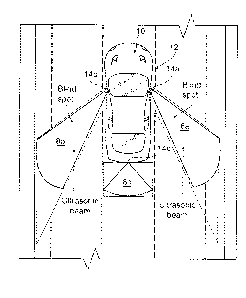
Reference may be had to Figure 1 which illustrates schematically a vehicle 10
having
an ultrasonic based obstruction monitoring system 12 in accordance with a
first embodiment.
The monitoring system 12 incorporates a series of ultrasonic sensors
assemblies 14a,14b,14c
which are each operable to emit and receive ultrasonic beam signals across a
respective vehicle
blind-spot or area of concern 8a,8b,8c, to detect adjacent vehicles and/or
nearby obstructions,
or encroachments in protected areas.
Each sensor assembly 14 is shown best in Figure 2 as incorporating an array of
twenty-five identical capacitive micromachined ultrasonic transducer (CMUT)
microarray
modules 16. As will be described, the microarray modules 16 are mounted on a
three-
dimensional base or backing platform 18, with the forward face or surfaces 19
of the
microarray modules 16 oriented in a generally hyperbolic paraboloid geometry.
Figure 2
shows best each of the CMUT microarray modules 16 in turn, as formed from
thirty-six
individual CMUT transducer/sensors 20 (hereinafter also transducers) which in
operation
output and receive a generally elongated ultrasonic signal beam (Figure 3). In
one
embodiment, transducers 20 are positioned within a 6x6 (not shown to scale)
rectangular or
square matrix or grid arrangement within the individual microarray module 16.
Figure 4b shows best, the three-dimensional backing platform 18 as constructed
as
having a number of module mounting surfaces 24 which are positioned at
selected levels LI,
L2,.. .L relative to each other in a discretized generally hyperbolic
paraboloid shape selected
to simulate the generally continuous curving hyperbolic paraboloid curvature
shown in Figure
19
CA 02857093 2014-05-27
WO 2014/066991
PCT/CA2013/000937
4a. In simplified form of manufacture, the backing platform 18 is formed as a
three-
dimensional plastic or silicon backing which presents twenty-five separate
discrete planar
square mounting surfaces 24 (Figure 4b). Each mounting surface 24 has a co-
planar
construction and a complimentary size selected to receive and support an
associated CMUT
microarray module 16 thereon. In this manner, the CMUT microarray modules 16
are
themselves mounted on the three-dimensional backing platform 18, with the
raised geometry
of the mounting surfaces 24 orienting the array of microarrays 16 in the
desired generally
discretized hyperbolic paraboloid geometry. The backing platform 18 is
provided with an
electrically conductive gold or copper top face coating layer 50 which
functions as a common
ground layer for each module transducer 20. The backing layer 18 in turn is
electrically gold
bonded to suitable pin connectors 32 (Figure 2) used to mount the pin base 34
as the sensor
chip 36 used in each sensor assembly 14a, 14b, 14c.
The applicant has appreciated that by varying the curvature simulated by the
relative
positioning of the mounting surfaces 24 in different hyperbolic paraboloid
configurations, it is
possible to vary the output beam geometry of the sensor chip 36, to tailor it
to a desired
application. By way of example, where the sensor assembly 14 is used as backup
vehicle
sensor 14c (Figure 1), the backing platform 18 may be provided with a flatter
hyperbolic
paraboloid curvature selected to produce comparatively wider, shorter beam
signals. In
contrast, sensor assemblies 14a,14b may be provided with a backing platform 18
having a
relatively higher degree of curvature, to output narrower, longer beam
signals.
In a most simplified construction, the 6x6 array of individual transducers 20
within
each CMUT microarray module 16 present a generally planar forward surface 19
(Figure 2)
which functions as a signal emitter/receptor surface for the generated
ultrasonic signals. In
use, the individual transducers 20 are electronically activated to emit and
then receive
ultrasonic beam signals which are reflected by nearby vehicles and/or
obstructions. In this
manner, depending on the timing between signal emission, reflection and
reception and/or the
intensity of the reflected ultrasonic signals which are detected by each
microarray module 16,
CA 02857093 2014-05-27
WO 2014/066991 PCT/CA2013/000937
the monitoring system 12 may be used to provide either an obstruction warning,
or in case of
auto-drive applications, control the vehicle operation speed and/or direction.
In the construction of each ultrasonic sensors assembly 14, each CMUT
microarray
module 16 used in the monitoring system 12 preferably is formed having a
footprint area of
about 1 to 5mm2, and a height of about 0.5 to 2mm. In the 5x5 matrix
arrangement shown in
Figure 2, the sensor chip 36 thus houses 900 individual transducers 20 in
twenty-five
microarray groupings of thirty-six, at seven discrete elevation levels, L17
(Figure 4b), in the
5x5 matrix distribution.
Figure 5 shows best an enlarged cross-sectional view of an individual
transducer 20
found in each CMUT microarray module 16 in accordance with a first
construction. In
particular, the transducer 20 is provided with a generally square-shaped
central air cavity or air
gap 42. The transducers 20 each have an average square lateral width dimension
davg selected
at between about 20 and 50[1m, and preferably about 30 m, with the interior
air gap 42
extending between about 60 and 80% of the lateral width of the transducer 20.
Preferably the
air gap 42 is defined at its lower extent by a silicon bottom wafer or layer
46, and which
depending on manufacture may or may not be provided with a coating. The air
gap 42 has a
height hg selected at between about 800 to 1000nm, and more preferably about
900nm. The air
gap 42 is overlain by 0.5 to l[tm, and preferably about a 0.8 tm thick silicon
device layer or
diaphragm membrane 44. A 0.1 to 0.2 [tm thick gold conductive layer 48 is
coated over the
diaphragm membrane 44 of the transducers 20 in each microarray module 16. The
conductive
layer 48 thickness is selected so as not to interfere with diaphragm 44
movement. In addition,
the bottom conductive coating 50 maybe provided either directly along a rear
surface of the
silicon bottom wafer or layer 46 of each transducer 20, or as described more
preferably is pre-
applied over each mounting surface 24 of the backing platform 18. In this
manner, by
electrically coupling the top conductive layer 48 of each microarray module 16
and the
conductive coating layer 50 on the backing platform 18 to a frequency
generator (shown as 70
in Figure 9), the diaphragm membranes 44 of the transducers 20 may be
activated to emit
and/or receive and sense generated ultrasonic signals.
21
CA 02857093 2014-05-27
WO 2014/066991 PCT/CA2013/000937
As shown best in Figure 3, where used in vehicular applications the individual
CMUT
microarray modules 16 are concurrently operable to transmit and receive a beam
signal at a
frequency at a range of between about 113-167 kHz. Most preferably in rain or
fog
environments the modules 16 operate with signal frequencies of about 150 kHz
13, and a
beamwidth of 20+5 with a maximum sidelobe intensity of -6dB. The sensor
microarray
module 16 may provide frequency independent broadband beam forming, without
any
microelectronic signal processing.
In one possible method of manufacture, the transducers 20 may be fabricated
using a
silicon-on-insulator (SOT) technology, with the three-dimensional backing
platform 18 formed
of silicon, and are assembled and packaged in a programmable gain amplifier
PGA-68 package
71. The present invention also provides for a more simplified method of
manufacturing the
three-dimensional hyperbolic paraboloid chip 36 construct, and more preferably
wherein the
hyperbolic paraboloid chip 36 functions with the hyperbolic paraboloid
geometry capacitive
micromachined ultrasonic transducer. In this regard, the three-dimensional
chip 36 may be
assembled using a backing platform 18 formed from plastic, and more preferably
acrylonitrile
butadiene styrene (ABS), that is formed to shape by means of a 3D printing
process. In an
alternate production method the 3D chip backing platform 18 may be formed by
injection
molding through micro-molding injection molding processes.
In manufacture, the backing platform 18 having the desired discretized formed
three
dimensional surface (and preferably formed of ABS plastic) is coated with a
suitable
conductive metal deposited coating layer 50 using sputtering, electroplating,
electroless
plating/coating, plasma coating and/or other metalizing processes. The mode of
metal
deposition is selected to enable placement of a continuous controlled layer of
conductive metal
over the top face of the ABS plastic backing platform 18, as formed. The
conductive metal
coating layer 50 is selected to provide a ground conductor for one side of the
transducers 20
within each microarray module 16. Preferred metals for deposition include
copper, gold,
silver, aluminum or other highly electrically conductive metals. Each CMUT
microarray
22
CA 02857093 2014-05-27
WO 2014/066991 PCT/CA2013/000937
module 16 is thereafter positioned and adhered with a conductive adhesive
directly on to an
associated mounting surface 24 in electrical contact with the conductive metal
coating layer 50
of the backing platform 18, with the backing platform 18 mounted to the pin
base 34 using pin
connectors 32.
While in a simplified construction, the forward face 19 of the transducer
sensors 20 in
each microarray module 16 provide a generally planar surface, the invention is
not limited. In
an alternate construction, the forward face 19 of each microarray module 16
may be provided
with or adapted for curvature. In such an arrangement, the transducers 20
within each of the
CMUT microarray module 16 are themselves assembled directly on a flexible and
compliable
bottom or backing substrate (not shown). Such a backing substrate is selected
from a material
and having a thickness to allow microarray module 16 to be flexed or bent to
better conform to
an actual 3D hyperbolic paraboloid surface as a continuous free-form surface,
as opposed to
stepped surfaces that approximate such a free-form surface. Preferred flexible
backings for the
microarray modules 16 would include the silicon wafer backings 46 themselves
having
thicknesses of less than about 5 1.ttn, and preferably less than 1 p.m, as
well as backing layers
made from CylothaneTM or bisbenzocyclobutene (BCB). Such
a free-form surface
advantageously also would allow the flexible backing of each CMUT microarray
module 16 to
be placed directly onto a free-form molded backing platform 18, providing the
sensor chip 36
with a more accurate approximation of an actual hyperbolic paraboloid surface
topography.
The inventor has recognized that when used as part of a vehicle monitoring
system 12,
the operating range of the CMUT microarray modules 16 may prove to have
increased
importance. Although not essential, preferably, to design for a specific
range, distance
damping and absorption attenuation of the air at the specific operating point
is determined.
Damping of sound is generally known to be calculated with the theory of the
air damping (air
resistance) as below:
PSI'Ldamping = ¨20 log10 (R1 / R2)
Where R/ is 30 cms for SPL standardization purposes, and R2 is the maximum
distance to
reach. For 5 m of distance, the ultrasound should travel 10 m. Solving the
equation yields -30
23
CA 02857093 2015-03-13
dB of damping in 10 m distance. Also, the absorption of the air due to
humidity is calculated
as follows:
a(f)= 0.022f ¨ 0.6 dB/ft
Where a is the air absorption due to frequency f The humidity is taken as 100%
for the worst
case scenario. Over the range of 10 m after conversion from ft, this
absorption value is
calculated to be -53 dB for 150 kHz.
It is therefore to be recognized when the total values there may exist
significant
damping of -83 dB. In contrast, the applicant has recognized that if the
transducers 20 were
operated in 60 kHz, total damping and absorption would be -51 dB, which will
allow a much
powerful received ultrasound signal.
In the construction of Figure 2, after obtaining the total damping and
absorption values,
the individual transducers 20 are designed accordingly. In particular, since
the total damping
values add up to -83 dB, the CMUT transducers 20 are most preferably designed
to have very
high output pressure, and most optionally 100 dB SPL or more. It has been
recognized that
preferably the diaphragm membrane 44 (Figure 5) of the CMUT transducers 20 is
chosen with
a thickness (TD) (Figure 5) less than 20 m, preferably less than 5pm, and most
preferably
about 11-LM. The selected membrane dimensions allow the diaphragm membrane 44
to have a
large distance for vibration, and a lower DC operating voltage.
Also following Mason's theory, (see Design of a MEMS Discretized Hyperbolic
Paraboloid Geometry Ultrasonic Sensor Microarray, IEEE Transactions On
Ultrasonics,
Ferroelectrics, and Frequency Control, Vol. 55, No. 6, June 2008, each CMUT
transducer 20 is
designed to operate over a frequency range of 110 to 163 kHz, and with the
sensor assembly
14 having twenty-five microarray modules 16 in accordance with specifications
shown in
Table 1. A most preferred operating frequency is selected at about 150 kHz
13, with the 5x5
array of CMUT microarray modules 16 designed with a 40 -3dB bandwidth and
side lobes
lower than -10Db, as shown in Figure 3. In this regard sound pressure can be
found following
the equation:
24
f
CA 02857093 2014-05-27
WO 2014/066991 PCT/CA2013/000937
= Re(Z,Oca4,
Where Aa is the amplitude of the acoustic wave, which is equal to the
displacement of the
CMUT membrane, co is the angular frequency of the diaphragm and Zn, is
acoustic radiative
impedance of the membrane obtained from Mason's method reference above.
Table 1 ¨ CMUT Sensor Array specifications - AUTOMOTIVE VEHICLE SENSOR
Parameter Value
Module Array 5x5
Array -3dB beamwidth (0) 400
Sensor sidelength (mm) 15.75
CMUT microarray module 1.6-1.8
sidelength (mm)
CMUT transducer diaphragm Low resistivity polysilicon
material
CMUT transducer sidelength (mm) 0.25-0.3
CMUT transducer diaphragm 0.5-1.0
thickness (vim)
CMUT transducer resonant 150 ( 13)
frequency (kHz)
CMUT transducer air-gap (pm) 2.5-4
Array pressure output (dB SAL) 102.5
CMUT bias voltage (VDc) 40
CMUT pull-in voltage (VDc) 51
CMUT receive sensitivity (mV/Pa) 60
Received signal at 10m (mV) 2
Table 1 above overviews the sensor array specifications of a prototype
automotive
vehicle sensor used as a backup sensor to provide obstruction warning signals.
Figure 6 illustrates an ultrasonic sensor assembly 14 in accordance with
another
embodiment of the invention, in which like reference numerals are used to
identify like
CA 02857093 2014-05-27
WO 2014/066991 PCT/CA2013/000937
components. In Figure 6, the ultrasonic sensor assembly 14 is provided with a
5x5 square
array of twenty-five CMUT microarray modules 16. Each of the CMUT microarray
modules
16 are in turn formed as a square 40x40 matrix of 1600 individual transducers
20 (not shown
to scale). While Figure 6 illustrates the sensor assembly 14 as including
twenty-five CMUT
microarray modules 16 arranged in a 5 matrix configuration, the invention is
not so limited. It
is to be appreciated that in alternate constructions, greater or smaller
number of microarray
modules 16 having fewer or more transducers 20 may be provided. Such
configurations would
include without limitation rectangular strip, generally circular and/or to the
geometric or
amorphous groupings of modules; as well as groupings of forty-nine or fifty-
four CMUT
microarray modules 16 mounted in 7x7, 9x9 or other square arrangements.
In one possible embodiment the 40x40 CMUT microarray modules 16 are secured to
an ABS backing platform 18 which has a geometry similar to that shown in
Figure 4b, and
which has been discretized in about a 2x2 mm, and preferably 1.7 x 1.7 mm flat
mounting
surfaces 24. In such a construction, the backing platform 18 is formed as an
approximated
hyperbolic paraboloid surface in the manner described above.
In an alternate design, the backing platform 18 is made as a substantially
flat ABS
construct, having a hyperbolic paraboloid curvature less than about 10 ,
preferably less than
about 10, and more preferably less than 0.50, wherein one or more of the
transducers 20
within each CMUT microarray module 16 is operable to more closely simulate
their mounting
in a hyperbolic paraboloid geometry. The microarrays modules 16 are
electrically bonded on
their rearward side 22 to the conductive metal coating layer 50 which has been
bonded as a
metal layer deposited on the ABS backing platform 18 in the manner as
described above. In
one construction, a top metal conductive layer 38, as shown in Figure 5, is
provided as the
second other power conductor for the CMUT transducers 20, allowing each
microarray 16 to
operate in both send and receive mode. As will be described however
alternatively transducers
20 each module 16 may be electrically connected in discrete groupings.
26
CA 02857093 2014-05-27
WO 2014/066991 PCT/CA2013/000937
Figure 7 shows an embodiment wherein each 40x40 microarray module 16 has a
square construction of between about I and 3 mm in sidewidth and contains
approximately
1600 transducers 20. As shown best in Figure 7 the transducers 20 are arranged
in a square
matrix orientation of parallel rows and columns within each microarray module
16. The
transducers 20 used in the module 16 of Figure 7 are shown best in the cross-
sectional view of
Figure 10 as having an average lateral width dimension davg selected at
between about 0.02 to
0.05mm and more preferably about 0.03 mm. Each transducer 20 defines a
respective
rectangular air gap 42 (Figure 10) which has a height hg of up to 3 nm and
preferably between
about 2.5 to 4 [tm, and width in lateral direction selected at between about
0.01 and 0.03 mm.
Figure 10 further shows best the transducers 20 as having a simplified
construction including
an etched silicon bottom wafer or backing layer 52, and which is secured by
way of a 0.5 to
20 [tm thick layer 54 of CycloteneTM or other suitable bisbenzocyclobutene
(BCB) resin layer
to an upper top silicon wafer 60. As will be described, the top wafer 60
defines the devices
diaphragm membrane 44, and has a thickness selected at between about 0.5 nm
and 1.0 nm.
In Figure 7 the gold conductive layer 30 is divided into individual,
electrically isolated
conductive gold wire strip bondings (W1,W2... WO. The
wire strip bondings WI,W2...Wn
provided across the diaphragm membranes 44 of aligned rows of transducers 20
and are each
selectively electrically connected to the frequency generator 70 by way of a
switching circuit
72.
In assembly, each 40x40 microarray module 16 is positioned as a discrete unit
on the
substantially flat substrate or backing layer 18. Within each individual 40 x
40 microarray
module 16, the transducers 20 are grouped into parallel strips or columns SI,
S2,...S40 (Figure
7). The transducers 20 in each column SI, S2,.. .S40, are electrically
connected to each other by
an overlaying associated conductive gold wire bonding W1, W2, W3¨W40. As shown
in
Figure 7, the gold wire bondings W1, W2, W3...W40 are in turn selectively
electrically coupled
to the conventional frequency generator 70 by way of a switching circuit 72
and
microprocessor controller 74. The frequency generator 70 is operable to
selectively provide
electrical signals or pulses at pre-selected frequencies. The applicant has
appreciated that the
activation of each individual or selected columns SI, S2.. .S40 of transducers
20 within each
27
CA 02857093 2014-05-27
WO 2014/066991 PCT/CA2013/000937
microarray 16 may change in the output wavelength of the sensor assembly 14 by
a factor of
approximately 0.1X. By activating the switching circuit 72 to selectively
switch power on and
off to different combinations of columns S1, S2.. .S40 of transducers 20 in
each microarray
module 16, it is possible to alter the signal shape of the transmitting signal
wavelength output
from the sensor assembly 14.
The generation of each electric pulse by the frequency generator 70 may thus
be used
to effect the physical displacement of the diaphragm membranes 44 of each
transducer 20
within one or more selected columns SI, S2.. .S40 electrically connected
thereto, by the
switching assembly 72, to produce a desired output ultrasonic wave frequency
and/or profile
having regard to the operation mode of the sensor assembly 14. The applicant
has appreciated
that in a most preferred configuration, signals are output from the sensor
assembly 14 at
wavelengths of between 110 kHz to 163 kHz, and preferably about 150 kHz. By
the selective
activation and deactivation of individual columns SI, S2.. .S40 of transducers
20 in each
microarray module 16, the output beamwidth and/or frequency, may be controlled
depending
upon the particular application requirement for the sensor system 12.
By example, Figures 8a to 8c show that depending upon the application
requirements
or mode of vehicle operation, it is possible to selective activate individual
transducers 20 in
each microarray module 16 to output a wider beam, where for example, the
sensor assembly
14 is used to provide warning signals in low speed back-up assist
applications. In addition,
different transducer 20 combinations in the same sensor assembly 14 may be
activated to
provide a narrower longer beamwidth, where for example, the vehicle is being
driven at
speed, and the sensor assembly 14 is operating to provide a blind-spot
warning, as for
example, during vehicle passing or lane change. In a most preferred mode of
operation, the
controller 74 is used to control the switching circuit 72 to activate the same
sequences of
columns SI, S2.. .S40 of transducers 20 within each of the CMUT microarray
module 16
concurrently during operation of the sensor assembly 14. This advantageously
may minimize
any adverse nodal effects and/or signal interference between signals output by
the individual
CMUT microarray module 16 within the sensor.
28
CA 02857093 2014-05-27
WO 2014/066991 PCT/CA2013/000937
In another mode of operation, the microprocessor controller 74 may be used to
activate the switching circuit 72 to selective actuate the columns Si, S2..
.S40 of transducers 20
in predetermined sequences to output signals of changing frequency. In yet
another mode, the
controller 74 may be used to activate the switching assembly 72 to initiate
one or more
individual columns SI, S2.. .S of specific transducers 20 within only selected
microarray
modules 16 within the 5x5 array. In this regard, the signals output by the
sensor assembly 14
may be coded or sequenced across a frequency range to more readily allow for
the
differentiation of third party sensor signals, minimizing the possibility of
cross-sensor
interference or false warning.
It is envisioned that the sensor assembly 14 shown in Figure 7 thus
advantageously
allows for programmable beamwidths to be selected at 20 and 140 or more, by
using the
controller 74 and switching circuit 72 to change the sensor output wavelength
dynamic.
While Figure 7 illustrates the transducers 20 within each CMUT microarray
module 16 as
being divided into forty separate columns Si, S2.. .S40, it is to be
appreciated that in alternate
configuration the transducers 20 in each microarray 16 may be further grouped
and/or
alternately individually controlled. In one non-limiting example, the
transducers 20 may be
further grouped and electrically connected by row, with individual columns
and/or rows
within each CMUT microarray module 16 being selectively actuatable by the
controller 74,
switching circuit 72 and frequency generator 70.
Figure 10 depicts a cross-sectional view of adjacent CMUT transducers 20 which
measure approximately 30x30 micrometers. In a more preferred construction, the
completed
CMUT microarray 16 will include 40x40 square matrix of 1600 CMUT transducers
20, and a
have a dimensional width of between about 1.7mm by 1.7mm. In an alternate
construction a
9x9 CMUT chip 36, may be provided with roughly 57600 individual CMUT
transducers 20.
29
CA 02857093 2014-05-27
WO 2014/066991 PCT/CA2013/000937
The sensor design provides for a 40x40 CMUT microarray modules 16 having a
square
configuration, with the sensor chip 36 having a dimension of about 7 to 10 mm
per side, and
which is machined flat or substantially for marginally hyperbolic with the
0.5 curvature.
Preliminary testing indicates that the ultrasonic sensor assembly 14 is
operable to transmit and
receive signals through solid plastic bumper materials having thicknesses of
upto several
millimeters, and without the requirement to have currently existing "buttons"
or collectors. As
such, the sensor assembly 14 may advantageously be "installed behind the
bumper" in
automotive applications, using smooth surfaced bumper panels, creating a more
aesthetically
pleasing appearance.
In operation, in receive mode (shown schematically in Figure 9) all of the
CMUT
transducers 20 preferably are activated to receive return beam signals to the
output at the same
time. The beam strength of the signals received, and/or the response time is
thus used to
determine obstruction proximity. In receive mode, the entirety of each CMUT
microarray
module 16 receives signals by impact which results in defection of the
transducer diaphragm
membranes 44 to generate receptor signals. The intensity and time of flight of
the return
signals detected by the degree of defection of each diaphragm membrane 44
provides an
indication as to the proximity of an adjacent obstruction and/or vehicle.
Transducer Manufacture
In a most preferred process of manufacture, benzocyclobutene (BCB) is provided
as
the structural component and/or the adhesive used in the manufacture of each
module 16 in
bonding of silicon and silicon-on-insulator (SOI) wafers. In particular, in a
simplified mode
of manufacture, sheets of transducers are formed by bonding together two
sheets of wafers to
simultaneously form multiple CMUT microarray modules 16, each having upto 1600
or more
CMUT transducers 20. After bonding, the wafers are then cut into separate the
individual
modules from the formed wafer sheet construct.
CA 02857093 2014-05-27
WO 2014/066991 PCT/CA2013/000937
One simplified mode of manufacture of each 40x40 microarray module 16 is
performed
largely as a two-component manufacturing process, as described with reference
to Figures 11
to 13. In manufacture, the microarray module 16 is prepared by joining an
etched silicon
wafer backing layer 80 (Figure 13) which is formed having individual
transducer air-gap
recesses or pockets 82 formed therein to a second covering silicon top wafer
60 using a BCB
resin layer 54.
In the formation of the first wafer backing layer 52, a removable silicon
holder piece 88
(not shown to scale) is provided. A dissolvable adhesive 62 is coated on the
silicon holder
piece 88, and a 0.5 to 2mm thick silicon layer 52 (Figure 11) is then secured
and mounted to
the holder piece 88. The silicon wafer backing layer 52 is next masked using a
photoresist
coating. The mask coating is applied to pattern the wafer backing layer 52
with the desired air
pocket 82 configuration of the desired transducer air gap arrays. After
exposure and activation,
the non-activated mask coating is removed to expose the selected air pocket
configuration and
wafer backing layer 63 for photo-plasma etching. The wafer backing layer 52 is
then photo-
plasma etched to a selected time period necessary to form the individual
pocket recesses 82
(shown in phantom in Figure 11). The pockets 82 are formed with a size and
desired spacing
to function as the air gap 42 of each transducer 20. The pockets 82 are
preferably formed with
a width of about 0.03mm in each lateral direction, and to a depth of about 2.5
to 4[tm.
Although not essential, the pockets 82 are preferably manufactured having a
square shape to
maximize their number of placement space on the backing layer 52. Other
embodiments could
however, include circular-shaped pockets or recesses 82 resulting in a larger
chip, and/or
pockets of a polygonal or hexagonal shape. The pockets 82 are preferably
formed in a square
matrix orientation to allow simplified transducer switching, however other
configurations are
possible. Etching is performed whereby at the bottom of each pocket 82, the
etched backing
layer 52 preferably has a thickness selected at about 0.5mm. Optionally, in an
alternate
manufacture, the wafer backing layer 52 may be inverted with the bottom of
each pocket 82
operating as the displaceable diaphragm membrane 44 of each CMUT transducer
20.
Preferably, however, the silicon top wafer 60 is provided as a top covering
layer with a desired
thickness selected to function as the displaceable diaphragm membrane 44.
31
CA 02857093 2014-05-27
WO 2014/066991 PCT/CA2013/000937
The top wafer 60 is separately formed. In a simplified construction, the top
wafer 60 is
machined from a preform by grinding to a desired thickness, and preferably a
thickness
selected at between about 0.2 to 2 gm. Following formation, the silicon wafer
60 is secured
to the etched backing layer 52 in position over top of the open pockets 82
using upto a 10 gm
thick, and preferably 0.05 to 1 gm thick adhesive layer 86 of BCB (Cyclotene)
resin as a
glue. Cyclotene provides various advantages. In particular, the use of the BCB
layer 86 acts
as an electrically insulating (non-conductive) layer. In addition, the
applicant has appreciated
that the BCB layer 86 advantageously allows for some deformation, enabling a
more
forgiving fit (upto 10vtm) between the etched bottom backing layer 52 and
the silicon top
wafer 60. This in turn advantageously allows for higher production yields with
more
consistent results.
Other possible substitutes adhesive layers may however, be used in place of a
Cyclotene adhesive layer 54, including silicon dioxide. Silicon dioxide and
heat bonding may
be used to fuse the silicon top wafer 60 to the etched silicon backing wafer
52. This however,
requires both surfaces to be joined to be very precisely machined to achieve
proper hard-
surface to hard-surface contact. In addition, silicon dioxide is less
preferred, as following the
joining of wafers 60,52, the silicon dioxide must be dissolved and drained
from each resultant
CMUT transducer air gap 42 cavity. This typically necessitates a further
requirement to drill
drain holes through each diaphragm membrane 44, which could later result in
moisture and/or
contaminants entering the transducers 20, leading to failure.
Following mounting of the silicon top wafer 60 on to the silicon bottom
backing layer
52, the top wafer 60 is laser ablated to the desired finish thickness to
achieve the membrane
diaphragm 44 (Figure 10), and preferably to a thickness of between 0.1 to 5
nm, and which
has flat uppermost surface. The final thickness of the top wafer layer 84 will
be selected
having regard to frequency range (thinner= lower frequency) of the output beam
signal.
32
CA 02857093 2014-05-27
WO 2014/066991 PCT/CA2013/000937
After laser ablating, a chromium interface layer 92 is optionally photoplated
onto the
top surface of the silicon wafer 60, and the adhesive 62 dissolved and holder
piece 68 then
removed. Optionally, the fused wafer assembly is thereafter cut to a desired
module size
having a desired number of individual transducers (i.e. 40x40). The conductive
gold layer 38
is then photo-printed onto the chromium layer 92 on the ablated top wafer 60.
The conductive
gold layer 38 provides electric conductivity from the frequency generator 70
to the metal
deposit layer 50 formed on the sensor backing platform 18. Where the sensor
assembly 14 is
to be provided with individually actuatable columns of transducers 20 SI, S2..
.S40 (as for
example is shown in Figure 7), after photo-printing of the gold layer 38, the
layer 38 is
thereafter selectively etched to remove and electrically isolate the portions
of the layer,
leaving behind the conductive gold wire bonding W1,W. = W40, which provide the
electrical
conductivity to the associated columns of transducers SI, S2.. .S40, In one
embodiment, the
completed CMUT microarray 16 is thereafter ready for direct robotic mounting
on the coated
metal surface 50 of the backing platform 18 by the use of an electrically
conductive adhesive
In an alternate mode of manufacture, the bottom of the etched silicon backing
layer 52
may be mounted directly on an electrically conductive base (not shown). In an
alternate
design, a single base may be provided which is made entirely of a conductive
metal, such as
copper or gold.
Yet another mode of manufacture, described with reference to Figures 5 and 14
to 19,
is performed as step-by-step fabrication process used to join a first silicon
wafer 80 as a
backing layer and a top silicon wafer 84 as device layer or membrane 44. In
accordance with
the method each cavity or pocket 82 (Figure 17) used to form each transducer
air gap 42 is
formed by removing portions of a BCB intermediate layer 104 which has been
secured to the
bottom silicon wafer layer 80. In such manufacture, a 4-inch N type silicon
wafer 80 is
provided as the backing layer wafer (Figure 14). The silicon wafer 80 is
heavily doped with
Antimony to achieve resistance in the range of 0.008 to 0.02 SI cm2.
33
CA 02857093 2014-05-27
WO 2014/066991 PCT/CA2013/000937
A 900 nm thick BCB layer 104 is spin deposited over the silicon base wafer 80,
following its coating its top surface 108 with a 1 nanometer thick layer 106
of AP3000TM as an
adhesion promoter layer 106. To prepare the surface for BCB coating, the
adhesion promoter
layer 106 is applied to the top surface 108 of the silicon wafer 80 (Figure
14) and then spun
dry. The resulting layer surface 106 is then immediately ready for BCB coating
to form
intermediate layer 104.
Following BCB coating, a 0.5 micrometer thickness Shipley 1805 photoresist
layer 110
(Figure 15) is then spin deposited on top of the BCB layer 104. After soft
baking of the
photoresist at 150 C, the photoresist layer 110 is exposed to UV light to
effect
photolithography and remove the desired parts of the layer 110 with the
location and geometry
of the where pockets 82 to be formed, exposing the underlying BCB layer 104,
as shown in
Figure 16. The BCB layer 104 is then dry etched using CF4/ 02 in a ICP
(Inductively Coupled
Plasma) reactor to form the pockets 82 in the pattern and orientation of the
desired transducer
air gap 42 configuration to be included in the microarray module 16, as shown
in Figure 17.
Figure 18 illustrates the top silicon wafer 84 as being provide as part of the
SOI silicon
covering wafer for bonding over the etched intermediate layer 104, and which
functions as a
transducer diaphragm membrane 44. To adhere the top wafer 84, a 1 nm thick
AP3000 layer
114 is deposited on a silicon top wafer layer 84 (optionally doped with
Antimony) having a
thickness of 0.8 1.tm. A further 200 nm thick BCB holder layer 118 is then
bonded to the
adhesion prompter layer 114 as a holder. The holder layer 118 is used in the
positioning of the
top wafer 84 as a cover. In the BCB layer 118, Cyclotene 3022-35 is most
preferably used as
the BCB adhesive and which is diluted by adding mesitylene.
In the final design, an active silicon wafer part of the silicon wafer 84 is
used as the
membrane 44 of each CMUT transducer 20, with the base wafer 80 forming the
bottom silicon
layer 46 (Figure 5). The base and silicon top wafers 80,84 are bonded using
the layer 104 of
BCB as bonding agent. The bonding process is preferably performed at 150 C to
drive out any
34
CA 02857093 2014-05-27
WO 2014/066991 PCT/CA2013/000937
residual solvents and to allow a maximum bonding strength. Bonded samples are
then cured at
250 C in nitrogen ambient for about 1 hour.
Optionally, one or more further adhesion promoter or coating layers may be
applied to
the base and/or top wafers 80,84 prior to bonding. Suitable coating layers
could include gold
or other conductive metal coatings.
Following wafer curing and bonding, the holder layer 118 is removed by
selectively
dissolving the adhesion product in adhesion promoter layer 114 using CF4 / H2,
leaving the top
silicon wafer 84 in place as the displaceable membrane 44. As a final step, a
100 nm thick
gold conductive layer 38 (Figure 5) is then deposited on to the top membrane
wafer 84. In an
alternate construction, the gold layer 38 may be spin deposited in place where
individual
activation of transducers 20 is not critical to the sensor assembly operation.
As a result, the embodiments of the sensor assembly 14 in accordance with
foregoing
embodiments feature one or more of the following:
1. The use or simulation of a 3D transducer configuration to shape and form
the sonic
beam;
2. An ultrasonic system using CMUT technology that uses or simulates a 3D
placement of
the CMUT transducers on a hyperbolic paraboloid surface to shape the beam;
3. The beam shape may be controlled by the design and shape of the hyperbolic
paraboloid shape of the chip, and which in turn controls the overall width of
the beam,
with the flatter the surface the wider the beam;
4. A hyperbolic paraboloid shape which limits the size and effect of minor
lobes, thus
producing less interference;
5. With the CMUT transducers it is possible to achieve greater signal
pressures in both
sending and receiving function;
6. Each CMUT transducer may be operated individually, in selected groupings;
and/or all
at the same time thus providing extensive capability of beam steering and
object
location within the beam; and
CA 02857093 2014-05-27
WO 2014/066991
PCT/CA2013/000937
7. The CMUT transducer design is smaller thus allows more transducers placed
on every
level thus more signal strength and resolution.
While the detailed description describes the transducers 20 in each microarray
module
16 as being electrically connected in a vertical strip configuration, the
invention is not so
limited. Other manner of coupling transducers 20 will also be possible. While
not limiting, it
is envisioned that a next generation, groupings of electrically coupled
transducers could be
oriented in both vertical strips as well as horizontal strips to allow for
frequency adjustment in
two directions.
While the monitoring system 12 in one preferred use is provided in vehicle
blind-spot
monitoring, it is to be appreciated that its application are not limited
thereto. Similarly, the
detailed description describes the capacitive micromachined ultrasonic
transducer-based
microarray modules 16 as being used as in automotive sensor 14, the invention
a variety of
other application will be readily apparent. Such applications include without
restriction,
applications in the rail, marine and aircraft industries, as well as uses in
association with
various household applications, industrial and commercial environments and in
consumer
goods.
While the description describes various preferred embodiment of the invention,
the
invention is not restricted to the specific constructions which are disclosed.
Many
modifications and variations will now occur to persons skilled in the art. For
a definition of
the invention, reference may be made to the appended claims.
36