Note: Descriptions are shown in the official language in which they were submitted.
CA 02858785 2014-06-10
1
ORGANIC MOLECULES FOR OLEDS AND OTHER OPTOELECTRONIC DEVICES
The present invention relates to the use of specific organic dyes without
metal centers as
emitters in OLEDs (organic light-emitting diodes) and in other optoelectronic
devices.
Introduction
Currently, it is apparent that OLED assemblies are already now of economic
significance,
since mass production is expected shortly. Such OLEDs consist predominantly of
organic
layers which can also be manufactured flexibly and inexpensively. OLED
components can
be configured with large areas as illumination bodies, but also in small form
as pixels for
displays.
Compared to conventional technologies, for instance liquid-crystal displays
(LCDs), plas-
ma displays or cathode ray tubes (CRTs), OLEDs have numerous advantages, such
as a
low operating voltage of a few volts, a thin structure of only a few hundred
nm, high-
efficiency self-illuminating pixels, high contrast and good resolution, and
the possibility of
representing all colors. In addition, in an OLED, light is produced directly
on application of
electrical voltage, rather than merely being modulated.
A review of the function of OLEDs can be found, for example, in H. Yersin,
Top. Curr.
Chem. 2004, 241, 1 and H. Yersin, õHighly Efficient OLEDs with Phosphorescent
Mate-
rials"; Wiley-VCH, Weinheim, Germany, 2008.
Since the first reports regarding OLEDS (see, for example, Tang et al., Appl.
Phys. Lett.
1987, 51, 913), these devices have been developed further particularly with
regard to the
emitter materials used, and particular interest has been attracted in the last
few years by
so-called triplet emitters or other phosphorescent emitters.
OLEDs are generally implemented in layer structures. For better understanding,
figure 1
shows a basic structure of an OLED. Owing to the application of external
voltage to a
transparent indium tin oxide (ITO) anode and a thin metal cathode, the anode
injects posi-
tive holes, and the cathode negative electrons. These differently charged
charge carriers
pass through intermediate layers, which may also consist of hole or electron
blocking lay-
ers not shown here, into the emission layer. The oppositely charged charge
carriers meet
CA 02858785 2014-06-10
2
therein at or close to doped emitter molecules, and recombine. The emitter
molecules are
generally incorporated into matrices consisting of small molecules or polymer
matrices (in,
for example, 2 to 10 % by weight), the matrix materials being selected so as
also to enable
hole and electron transport. The recombination gives rise to excitons (=
excited states)
which transfer their excess energy to the respective electro-luminescent
compound. This
compound can then be converted to a particular electronic excited state which
is then con-
verted very substantially, and with substantial avoidance of radiationless
deactivation
processes to the corresponding ground state by emission of light.
With a few exceptions, the electronic excited state, which can also be formed
by energy
transfer from a suitable precursor exciton, is either a singlet or triplet
state. Since the two
states are generally occupied in a ratio of 1:3 on the basis of spin
statistics, the result is
that the emission from the singlet state, which is referred to as
fluorescence, according to
the present state of the art, leads to maximum emission of only 25 A of the
excitons pro-
duced. In contrast, triplet emission, which is referred to as phosphorescence,
exploits and
converts all excitons and emits them as light (triplet harvesting), such that
the internal
quantum yield in this case can reach the value of 100 %, provided that the
additionally ex-
cited singlet state which is above the triplet state in terms of energy
relaxes fully to the trip-
let state (intersystem crossing, ISC), and radiationless competing processes
remain insig-
nificant. Thus, triplet emitters, according to the current state of the art,
are more efficient
electro-luminophores and have better suitability than purely organic singlet
emitters for
ensuring a high light yield in an organic light-emitting diode.
In the triplet emitters suitable for triplet harvesting transition metal
complexes are generally
used in which the metal is selected from the third period of the transition
metals. This pre-
dominantly involves very expensive noble metals such as iridium, platinum or
else gold.
(See also H. Yersin, Top. Curr. Chem. 2004, 241, 1 and M. A. Baldo, D. F.
O'Brien, M. E.
Thompson, S. R. Forrest, Phys. Rev. B 1999, 60, 14422).
The phosphorescent organometallic triplet emitters known to date in OLEDs,
however,
have a disadvantage, which is that these complexes are frequently more
chemically reac-
tive in electronically excited states than in the base states. Responsible for
this are gener-
ally metal-ligand bond breakages. Therefore, the long-term stability of these
emitter mate-
rials is inadequate in many cases. (T. Sajoto, P. I. Djurovich, A. B. Tamayo,
J. Oxgaard,
CA 02858785 2014-06-10
3
W. A. Goddard III, M. E. Thompson; J. Am. Chem. Soc. 2009, 131, 9813). As a
result,
efforts are being made to develop emitter molecules without metal centers and
with high
emission quantum yield, wherein the emitter molecules shall furthermore also
convert all
singlet and triplet excitons into light. OLEDs using such emitters should
exhibit a high effi-
ciency, and additionally enable a longer lifetime of the optoelectronic
device.
In summary, the prior art can be described such that the triplet emitters
which are efficient
per se and are known to date have the disadvantages that
- expensive noble metal molecules have to be used
and that
- these emitters formed on the basis of organometallic complexes have
only inadequate
long-term stability in many cases.
Description of the invention
Surprisingly, the problems described above can be significantly improved or
solved by the
present invention, using organic molecules (dyes, emitter molecules) which
have particular
electronic structures or singlet-triplet energy separations and which are
modified in accor-
dance with the invention by changes in the immediate environment of the
emitters. This
process of 'singlet harvesting for organic emitters" which is proposed here
for the first time
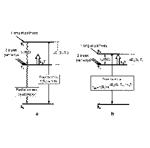
is to be described briefly below using figure 2:
Fig. 2a shows a (simplified) energy level scheme for a typical, purely organic
molecule
having a AE(S1-T1) value between the lowermost excited singlet state (Si) and
the triplet
state (Ti) below it of clearly greater than 3000 cm-1.
Using this scheme, the photophysical electroluminescence properties of these
molecules
can be illustrated. Hole-electron recombination, as occurs, for example, in an
optoelectron-
ic component, leads, on statistical average, to 25 % occupation of the singlet
state and to
75 % occupation of the three sub-states of the triplet state. Since the
emission transition
from the triplet state Ti to the singlet state So is strongly spin-forbidden
in organic mole-
cules due to the low level of spin-orbit coupling, the excitation energy which
arrives at the
triplet state is generally converted radiationlessly to heat and is thus been
lost for the light
production by electroluminescence. The occupied singlet state can, however,
exhibit effec-
=
CA 02858785 2014-06-10
4
tive emission (fluorescence) because this is a spin-allowed singlet-singlet
transition. In this
context, it is important to mention that the radiationless relaxation process
from the S1
state to the Ti state, called the intersystem crossing (ISO) process, is
likewise strongly for-
bidden due to the low level of spin-orbit coupling. Otherwise, no fluorescence
would be
observable. For the time constants, this means that ii(ISC) is several orders
of magnitude
longer than the fluorescence lifetime, which is in the region of one to a few
nanoseconds
for T(Si).
According to the invention, the above-described disadvantages of the prior art
can be
avoided. This is possible by a combination of two steps:
I. Organic molecules with high emission quantum yield (greater than 50 %)
are pro-
vided, for which the energy difference between the singlet S1 and the triplet
T1 is
sufficiently small than thermal repopulation from the triplet Ti to the
singlet S1 is
possible at room temperature, as a result of which the triplet excitation can
be con-
verted to light via the singlet S1 state. This is achieved according to the
invention
using purely organic molecules, for instance using organic molecules of the
formu-
lae I, II, Ill, IV and/or V.
II. The extremely long intersystem crossing time constant (T(ISC)) of
purely organic
molecules is shortened by a few orders of magnitude in order to enable
sufficiently
rapid thermal repopulation, the so-called up-intersystem-crossing. This is
possible
by virtue of enhancement of spin-orbit coupling, in particular by additional
introduc-
tion of atoms or molecules which have a high level of spin-orbit coupling. The
in-
crease of the spin-orbit coupling can also result from covalent bonding of an
addi-
tive to the emitter molecule. These effects are known to the chemist as
"external" or
"internal heavy atom effect". This process is explained further below.
Using these two strategies, which are to be used together ¨ as illustrated by
figure 2b ¨
the triplet and singlet excitations populated in the electroluminescent
excitation can be col-
lected and converted to light via the singlet state S1. This process
exploiting the singlet
harvesting effect for organic molecules, which is described here for the first
time, is ex-
plained in detail hereinafter.
5
Accordingly, the invention, in one aspect, provides a composition, especially
for utilization
in an optoelectronic device, which comprises
- an organic emitter molecule having a lowest excited singlet state (Si) and a
triplet state
(Ti) below it, the AE(Si-Ti) value of the organic molecule being less than
3000 cm-1 (pref-
erably smaller than 2500 cm-1), in particular between 10 cm-1 and smaller than
3000 cm-1,
and
- an optically inert atom or molecule which interacts with the organic
molecule such that
the intersystem crossing time constant of thermal repopulation, i.e. the up-
intersystem
crossing time constant, of the organic molecule is reduced to less than 300
ms, preferably
.. to less than 1 ms, more preferably to less than 1 ps. In a preferred
embodiment, this is
accomplished by an optically inert atom or molecule, which has, or by
molecular compo-
nents which have a high level of spin-orbit coupling. This can be described by
the spin-
orbit coupling constant, which should be higher than about 200 cm-1,
preferably higher
than 1000 cm-1 and more preferably higher than 2000 cm-1, most preferably
greater than
4000 cm-1.
The terms "spin-orbit coupling constant" and "intersystem crossing time
constant" and "up-
intersystem crossing time constant" are specialist terms which are commonly
used in the
photophysical literature and are therefore known to those skilled in the art.
According to a further aspect of the invention, there is provided a
composition comprising
- an organic molecule for emission of light which has a AE(Si-Ti) value
between the
lowest excited singlet state (Si) and the triplet state (Ti) below it of less
than 3000 cm-1,
and
- an atom or a molecule for reduction of the intersystem crossing time
constant of
the organic molecule to less than 300 ms,
wherein the organic emitter molecule is a molecule of formula V:
CA 2858785 2018-12-11
5a
D2 D1 D5 D6
D3 II.. D7
D4 D8
Al A8
A2 A7
A3 A4 A5 A6
Formula V
wherein
D1 to D8 are, independently from each other, H, Br, I and/or groups, which
represent a donor D;
the donor groups may be same or different;
at least one donor group is present;
wherein adjacent Di, Dj and Dk from D1 to D8 are optionally conjugated
aromatic or
heteroaromatic rings, optionally comprising a donor function;
Al to A8 are independently from each other H, Br, I and/or groups, which
represent
an acceptor A;
wherein adjacent Ai, Aj and Ak from Al to A8 are optionally conjugated
aromatic or
heteroaromatic rings, optionally comprising an acceptor function;
wherein the acceptor groups may be same or different; and
at least one acceptor group is present; and
wherein Br and/or I is optionally bound to the organic molecule of formula V
via an
alkyl group (with C = 1 or 2), and
wherein the optically inert atom or molecule is selected from the group,
consisting of
krypton, xenon, bromine-comprising substances, iodine-comprising substances,
metal
atoms, metal nanoparticles, metal ions, gadolinium-complexes and lead
complexes.
CA 2858785 2018-12-11
5b
Molecules with small AE(Si-T1)-separations
Fig. 2b shows an energy level diagram for an organic molecule having a small
energy dif-
ference AE(Si-T1) <3000 cm-1. This energy difference is small enough to enable
thermal
repopulation of the Si state from the Ti state according to a Boltzmann
distribution, or ac-
cording to the thermal energy kBT, and hence thermally activated light
emission from the
Si state. This process, which is referred to as thermally activated (delayed)
fluorescence,
is simplified controlled by equation (1)
Int(Si ¨> So) / Int(Ti So) = k(S1) / k(Ti) exp(-
AE/kBT) (1)
In this equation, Int(Si --> So)/Int(T1--> So) is the intensity ratio of the
emissions from the Si
state and the Ti state. kB is the Boltzmann constant and T the absolute
temperature.
k(Si)/k(-11) is the rate ratio of the conversion processes from the singlet Si
and from the
CA 2858785 2018-12-11
CA 02858785 2014-06-10
6
triplet T1 to the electronic ground state So. For organic molecules, this
ratio is generally
between 106 and 1010. Preference is given in accordance with the invention to
molecules
having a rate ratio of about 107, better of about 109, more preferably of
about 1010. AE
represents the energy difference AE2(S1-Ti) according to figure 2b.
Through the process of thermal repopulation described, an emission channel is
opened up
from the populated triplet via the singlet state S1. Since the transition from
the S1 to the So
state is strongly allowed, the triplet excitation energy, which is otherwise
lost, is obtained
virtually completely as light emission via the singlet state, At a given
temperature, for ex-
ample at room temperature, the smaller the energy difference AE, the more
marked this
effect is. Preference is therefore given to organic molecules having a AE =
AE(Si--11) value
between the lowermost excited singlet state and the triplet state below it of
less than
3000 cm-1, better less than 2500 cm-1 or 1500 cm-1, preferably of less than
1000 cm-1.
This effect is to be illustrated by a numerical example. Given an energy
difference of AE =
1300 cm-1, for room temperature applications (T = 300 K) with kBT = 210 cm-1
and a rate
ratio of 108, an intensity ratio of the singlet to triplet emission according
to equation (1) of
approx. 2.105 is obtained. This means that the singlet emission process is
dominant to an
extreme degree for a molecule having these example values.
The applicability of equation (1) requires according to the invention the use
of additives
which increase spin-orbit coupling (for detailed arguments see, for example,
below). These
additives, i.e. optically inert atoms or molecules of the composition,
interact with the organ-
ic emitter molecules such that the mean (thermalized) emission lifetime of the
two states
S1 and T1 of the organic molecule is strongly reduced. Preference is given to
compositions
of such a kind that the emission lifetime is reduced to less than 500 ms,
preferably to less
than 1 ms, particularly preferably to less than 20 ps, more preferably to less
than 10 ps
and most preferably to less than 1 ps. It is essential that the time of the
thermally activated
reoccupation from the T1 state is shorter (e.g. by factor 5) than the
phosphorescence de-
cay time T(Ti) without thermal reoccupation. This decay time T(1-1) can be
easily detected
at low temperatures, e.g. at 77 K, with commercial measurement instruments.
CA 02858785 2014-06-10
7
In summary, using this "singlet harvesting process for organic molecules", it
is thus possi-
ble in the ideal case to capture virtually all, i.e. a maximum of 100 %, of
the excitons and
convert them to light via singlet emission. In addition, it is possible to
shorten the emission
decay time well below the value for purely organic triplet emitters, which is
a few seconds.
Therefore, the inventive composition is particularly suitable for
optoelectronic components.
Organic molecules having the above-described properties, i.e. having a small
singlet-triplet
energy difference AE (S-1-Ti), are preferably organic molecules having the
following gener-
al formulae Ito III:
B A)
Formula I
D
Formula II
A
Formula III
In these formulae, D is a chemical group or a substituent with an electron-
donating effect
(D, donor effect). Substituents of this kind may be present once, twice or
several times.
They may be the same or different.
CA 02858785 2014-06-10
8
A is a chemical group or a substituent with an electron-withdrawing property
(A, acceptor
effect). Substituents of this kind may be present once, twice or several
times. They may be
the same or different.
The base structure B is composed of conjugated organic groups which consist
for example
of aromatic, heteroaromatic and/or conjugated double bonds. In one embodiment,
the
base structure can also represent a non-conjugated group. It is essential that
the molecule
orbitals of A and B or of D and B cover the same area. The base structure B
itself can also
have an electron withdrawing effect, then (e.g. in formula I) the substitution
can have D
character on both sides. Alternatively, the base structure B itself can have
an electron do-
nating effect, then (e.g. in formula I) the substitution can have A character
on both sides.
The formulas Ito III represent also that the electronic wave functions of the
molecules
overlap in the areas D/B or B/A. This characteristic can be determined by
calculations as
described further below. The term electronic wave function is known to the
person skilled
in the art.
Examples of donors D:
-0(-), -NH-alkyl group, -N-(alkyl group) 2 -NH2, -OH, -0-alkyl group, -
NH(CO)alkyl
group, -0(C0), - alkyl group, -aryl group, -heterocyclic groups -(CH)=C-(
alkyl group)2, -
phenoxazinyl, -phenothiazinyl, -carbazolyl, -dihydrophenazinyl, -N(R")(R")
with (R', R" =
H, alkyl, aryl, halogenated alkyl, halogenated aryl), all aryl and
heterocyclic groups can be
substituted with alkyl and/or aryl groups, all alkyl groups can also be
substituted with F, CI,
Br and/or I.
Examples of acceptors A:
-halogen, -(CO)H, -(C0)-alkyl group, -(C0)0-alkyl group, -(C0)0H, -(CO)CI, -
CF3, -BF2,
-CN, -S(0)20H, -S(0)20-alkyl, -NH3,-N(alkyl group)3+, -NO2, halogenated alkyl,
-B(R")(R") with (R", R" = H, alkyl, aryl, halogenated alkyl, halogenated
aryl).
Composition of the base structure B:
B is composed of conjugated organic groups which consist of aromatic,
heteroaromatic
and/or conjugated double bonds. In certain embodiments, molecular base
structures B
have aromatic or heteroaromatic rings smaller than 15, more preferably smaller
than 10,
CA 02858785 2014-06-10
9
most preferably smaller than seven. The aromatic or heteroaromatic rings are
chemically
joined directly or chemically bound via alkenyl groups having conjugated
double bonds
smaller than 10, more preferably smaller than six and most preferably smaller
than 3. In
one embodiment, the base structure can also represent a non-conjugated group.
It is es-
sential that the molecule orbitals of A and B or of D and B cover the same
area.
The organic molecules described by formulas Ito III have AE(Si-T1) values
between the
lowermost excited singlet state and the triplet state below it of less than
3000 cm-I, prefer-
ably less than 2500 cm-1 or 1500 cm-1 and more preferably less than 1000 cm-1.
Processes
for measurement or calculation of the E(S -T1) values are discussed below.
Preference is given to organic molecules which, without use of additives, have
a high fluo-
rescence quantum yield from the Si state of greater than 30 %, preferably
greater than
50 cY0, more preferably greater than 80 % (determination with commercial
measuring in-
struments for emission quantum yield) and for which the absorption
intensities, i.e. the mo-
lar decadic extinction coefficients, of the transitions between the ground
state So and the
excited state Si are greater than 1031/mol cm, preferably greater than 104
limol cm, more
preferably greater than 5x10⁴ I/mol cm (determination with commercial
absorption spec-
trometers).
The invention relates, in a further aspect, to a process for selecting organic
molecules for
which the AE(Si-T1) value between the lowermost excited singlet state (Si) and
the triplet
state (T1) below it is less than 3000 cm-1, preferably less than 2500 cm-1 or
1500 cm-1, par-
ticularly preferably less than 1000 cm-1.
The determination of the AE(Si-Ti) value can either be performed by quantum-
mechanical
calculations using known computer programs (for example executing TDDFT
calculations,
for example using commercially available Gaussian 09 or ADF-Amsterdam Density
Func-
tional Software programs) or determined experimentally, as explained below.
Information
for a first orientation can already be gained from comparatively easily to
conduct DFT cal-
culations (e.g. with commercially available Gaussian 09 or ADF-Amsterdam
Density
Functional Software Program). Here, for example, the frontier orbitals HOMO-2,
HOMO-1,
HOMO, LUMO, LUM0+1 und LUM0+2 show tendencies of the charge transfer
properties
CA 02858785 2014-06-10
=
to expect with regard to the lowest excited energy states of the molecules. In
the following
paragraph these properties are described.
The energy difference AE(S1-T1), more particularly of the organic molecules
described by
5 formulas Ito III, can be described as an approximation by quantum-
mechanical means via
the exchange integral multiplied by the factor 2. The value of the latter
depends directly on
the overlap of the molecular orbitals in the area on the D side of B with the
molecular or-
bitals in the area on the A side of B (formula l). Accordingly, the value of
the exchange
integral is determined by the overlap of the wave functions in the D-B area
(formula II) or
10 the A-D area (formula ill) with those in the B area. Due to the
properties of D and A de-
scribed above, these molecular orbitals are distributed over different spatial
areas (partly
delocalized over it or 7C* molecular orbitals). This means that an electronic
transition be-
tween the different molecular orbitals represents a charge transfer (CT)
process or a
process with CT involvement within the molecule. The target small exchange
integral and
thus a small energy difference AE(Si-Ti) can be achieved with an organic
molecule which
has the corresponding CT character with regard to the lowest excited molecule
orbitals,
wherein the molar decadal extinction coefficients for the electronic
transition from So to S1
also lie in the preferred range defined above. In other words, AE(Si-Ti) can
be varied via
the strengths of the electron-donating and -withdrawing substituents/groups of
the organic
molecule. Due to these photophysical (quantum-mechanical) properties, it is
possible to
achieve the inventive energy differences with AE(Si-Ti) of less than 3000 cm-1
or less than
2500 cm-1 or less than 1500 cm-1 or less than 1000 cm-1.
The AE(S1-T1) value can be determined experimentally as follows:
For a given organic molecule, the energy separation AE(S1-T1) = AE can be
determined in
a simple manner using the above-specified equation (1). A rearrangement
yields:
InfInt(S1-->S0)/Int(T1¨>S0)} = In {k(Si)/k(Ti)} ¨(AE/k8)(1/T) (2)
For the measurement of the intensities Int(S1¨>S0) and Int(Ti--+So), it is
possible to use any
commercial spectrophotometer. A graphic plot of the (logarithmic) intensity
ratios
In{Int(S1¨>S0)/Int(T1-->S0)} measured at different temperatures against the
reciprocal of the
CA 02858785 2014-06-10
11
absolute temperature T generally yields a straight line. The measurement is
conducted
within a temperature range from room temperature (300 K) to 77 K or to 4.2 K,
the temper-
ature being established by means of a cryostat. The intensities are determined
from the
(corrected) spectra, Int(S1-->S0) and Int(Ti¨>S0) representing, respectively,
the integrated
fluorescence and phosphorescence band intensities, which can be determined by
means
of the programs provided with the spectrophotometer. The respective
transitions (band
intensities) can be identified easily since the triplet band is at lower
energy than the singlet
band and gains intensity with falling temperature. The measurements are
conducted in
oxygen-free dilute solutions (approx. 10-2 mol L--1) or on thin films of the
corresponding
molecule or on films doped with the corresponding molecules. If the sample
used is a solu-
tion, it is advisable to use a solvent or solvent mixture which forms glasses
at low tempera-
tures, such as 2-methyl-THF, THF (tetrahydrofuran) or aliphatic hydrocarbons.
If the sam-
ple used is a film, the use of a matrix having a much greater singlet and
triplet energy than
that of the organic emitter molecules, for example PMMA (polymethyl
methacrylate), is
suitable. This film can be applied from solution. It is particularly important
that, as de-
scribed below, the molecules to be analyzed are used with the respective
additives.
The slope of the straight line is ¨AE/kB. With kB = 1.380 = 10-23 JK-1 = 0.695
cm-1 K-1, it is
possible to determine the energy separation directly.
An equivalent approach shows that it is also possible to determine the AE(Si-
Ti) value by
means of the temperature dependence of the emission decay time.
A simple, approximate estimation of the AE(S1-T1) value can also be made by
recording
the fluorescence and phosphorescence spectra at low temperature (e.g. 77 K or
4.2 K us-
ing a cryostat). The AE(S1-T1) value then corresponds approximately to the
energy differ-
ence between the high-energy slope flanks of the fluorescence band and the
phosphores-
cence band, respectively.
The More marked the CT character of an organic molecule, the greater the
variation in the
electronic transition energies as a function of solvent polarity (cf. e.g. J.
B. Birks, Photo-
physics of Aromatic Molecules, Wiley-lnterscience, London 1970; E. Lippert, Z
Natur-
forsch. 10a (1955) 541). For instance, the evidence of a marked polarity
dependence of
CA 02858785 2014-06-10
12
the emission energies provided by a simple measurement already indicates the
presence
of a CT-transition and thus indicates small AE(Si-11) values.
Moreover, it is important to reduce the radiationless processes (rates),
because it leads to
an increase of the emission quantum yields of the emitter molecules.
- For instance, in one embodiment of the invention, the protons of the emitter
molecules
are partly or completely replaced by deuterium.
- In an optional embodiment, deuterizing or partly deuterizing the matrix
of the optoelec-
tronic device can in particular cases also lead to a distinct increase of the
emission quan-
turn yield.
- Another method for the reduction of the radiationless processes, i.e. for
increasing the
emission quantum yield of the emitter molecules, consists in shaping the
direct environ-
ment as rigid as possible by selecting e.g. a polymer matrix or a polymer
cross-linked ma-
trix or a semi-crystalline matrix. Strategies of polymer cross-linking are
known to a person
of skill in the art (see e.g. C. A. Zuniga, S. Barlow, S. R. Marder; Chem.
Materials 2011,
23, 658-681). The matrix used in the examples, glucose-trehalose, meets this
demand of
rigidity.
Additives / Reduction of the intersystem crossing time constant
Preferred organic molecules consist exclusively of light atoms such as C, H,
N, 0, F, S, K,
Na. For such organic molecules, the electronic singlet and triplet states of
which result es-
sentially from transitions between Tr and TC* molecular orbitals, the
effective spin-orbit
coupling (SOC), as already mentioned, is so small that the relaxation
transitions from the
Si to the energetically lower Ti state (down-intersystem crossing) and in the
reverse direc-
tion from the TI state to the S1 state (up-intersystem crossing) are strongly
forbidden or
barely occur.
According to the invention, this is no longer forbidden: the organic molecules
(emitter mo-
lecules), especially those of formulas I, II and ill, as well as according to
formulas IV and
V, may be doped, for example, into optoelectronic devices, or into matrix
materials, for ex-
ample in an OLED emission layer. According to the invention, optically inert
atoms or mo-
lecules (so-called "additives") are mixed into this matrix to reduce the
intersystem crossing
time constant of the organic molecule. These optically inert atoms or
molecules are nota-
CA 02858785 2014-06-10
13
ble for high spin-orbit coupling (SOC) (SOC constant of the atoms or molecular
units
greater than 1000 cm-1; see the explanations given further below). These
additives are
introduced, for example, in a concentration corresponding approximately to or
higher than
that of the emitter molecules. These additives can, for example, also be used
in a concen-
tration twice to ten times as high as that of the organic emitter molecules.
In general, the
numeric ratio between organic emitter molecules and optically inert atoms or
molecules is
1:0.1 to 1:5 or 1:10, preferably 1:0.2 to 1:5, more preferably 1:1. This gives
rise to such a
distribution probability that at least one additive particle/additive molecule
having high SOC
is present in the immediate environment of an emitter molecule. This induces
external
SOC, which strongly accelerates the process of intersystem crossing, i.e. the
time constant
of the intersystem crossing is shortened accordingly. This brings about very
rapid relaxa-
tion from the Si to the T1 state and likewise a very rapid thermal
repopulation according to
equation (1). This enables the singlet harvesting effect for organic
molecules.
According to the invention, it is also possible to change the matrix with
suitable SOC in-
creasing substituents; e.g. the matrix polymers can comprise chemically bound
Br or I
atoms, and thus, the matrix adopts the function of the additive. Likewise, the
emitter mole-
cules can comprise e.g. chemically bound Br or I atoms or other substituents
increasing
the SOC. In these particular cases, the amount of the additive can be highly
reduced or
the addition of an additive can be completely dispensed with under favorable
conditions.
Accordingly, the present invention relates in one embodiment to a composition
comprising
an organic molecule for the emission of light, which has a AE(Si-T1) value
between the
lowest excited singlet (Si) and the triplet state (Ti) below it of smaller
than 3000 crn-1 (pre-
ferably smaller than 2500 cm-5, and an optical inert atom or an optical inert
molecule for
reducing the up-intersystem crossing time constant of the organic molecule to
less than
300 ms, wherein the optical inert atom or an optical inert molecule is
chemically bound to a
matrix, in particular to a polymeric matrix.
Examples of the additives are:
= Noble gases (especially preferred):
Krypton (Kr), but more preferably xenon (Xe).
These gases are introduced during the process for producing an optoelectronic
corn-
CA 02858785 2014-06-10
14
ponent into the matrix, which has been doped with the emitter molecules and is
used
to form the emission layer. It is necessary in this context to ensure gas
saturation at a
gas pressure of 1 atmosphere (1013.25 hPa), optionally under elevated gas
pressure
of up to about 3 atm (approx. 300 kPa), for example of about 2 atm (approx.
200 kPa). The emission layer is applied under this gas atmosphere, for
example, by
means of spin-coating or other wet-chemical processes.
= Bromine- and iodine-containing substances, particular preference being
given to
iodine-containing substances.
Br- or particularly preferably I-containing substances are added to the
solution used to
produce the emission layer of an optoelectronic component, for example, alkyl
bro-
mides, alkyl iodides (e.g. ethyl iodide, propyl iodide), aryl bromide, aryl
iodide (e.g.
naphthyl iodide).
Optoelectronic devices using these additives are produced by wet-chemical
means.
= The matrix material of the emission layer of an optoelectronic component
may consist
of bromine-containing substances, but particularly preferably of iodine-
containing sub-
stances or polymer-bound Br or I, or comprise these substances (e.g. poly(4-
iodostyrene). The halogens may also be present in chemically bound form in the
po-
lymer side groups.
Optoelectronic devices using these additives are produced by wet-chemical
means.
= Suitable additives are also nanoparticles of metal atoms of the second or
preferably
third period of the transition metals, or gadolinium.
Optoelectronic devices using these additives are produced by wet-chemical
means or
by means of vacuum or vapor phase deposition processes.
= Preferred additives are Gd complexes. These can be added to the solutions
of the
emission layers used in the production for wet-chemical processing operations,
or co-
vaporized in the case of production of the optoelectronic devices by means of
vacuum
sublimation or vapor phase deposition. Particular preference is given to
chemically
stable Gd complexes which are optically inert within the spectral range
required for
the application. Examples are: Gd(cyclopentadiene)3,
Gd(tetramethylheptadiene)3, Gd
acetate, Gd(acac)3, Gd(TMHD)3, Gd 2-ethylhexanoate, etc. Gd ions are
considered
to be optically inert and can be used in a further aspect of the invention.
For example,
these Gd ions can also enter into chemical bonds with the organic emitter
molecules.
CA 02858785 2014-06-10
Gd complexes can be formed, for example. Lead compounds are referred to as fur-
ther additives, e.g. Pb(CH3C00)2.
= Suitable additives are generally atoms or molecules or nanoparticles
which do not
have any absorptions or emissions in the emission region or relevant HOMO/LUMO
5 region of the emitter, and hence are considered to be optically inert
within these re-
gions. The additives, or the atomic constituents thereof, should also have a
high SOC
constant which is preferably greater than 1000 cm-1, more preferably greater
than
3000 cm-1, most preferably greater than 4000 cm-1.
10 .. OLED devices as optoelectronic devices
In a further aspect of the invention, the composition described here is used
in an emitter
layer in an optoelectronic (organic electronic) device, especially an OLED.
The OLED devices can be produced by processes known in the art (cf. H. Yersin,
"Highly
15 Efficient OLEDs with Phosphorescent Materials", Wiley-VCH, Weinheim,
Germany 2008).
In a preferred embodiment of an organic light-emitting diode (OLED), the
proportion of the
composition (organic emitter and additive) in the emitter layer is between 2 %
by weight
and 100 % by weight, preferably between 6 % by weight and 30 % by weight.
Further optoelectronic devices
Another aspect of the invention refers to the use of the inventive composition
composed of
an organic molecule and an optically inert atom or optically inert molecule in
light-emitting
electrochemical cells (LEECs), OLED sensors (e.g. OLED oxygen sensors),
especially in a
gas and vapor sensor not hermetically sealed from the outside, optical
temperature sen-
sors, organic solar cells (OSCs; organic photovoltaics, OPVs), organic field-
effect transis-
tors, organic diodes, organic photodiodes and "down conversion" systems.
Generally, the proportion of the composition in an emitter layer of an
optoelectronic device
may be 2 to 100 % by weight, preferably 6 to 30 `)/0 by weight, based on the
total weight of
the emitter layer.
In a further aspect, the invention relates to a process for reducing the
(radiative) emission
lifetime and to a process for increasing the electroluminescence quantum yield
of an or-
CA 02858785 2014-06-10
16
ganic molecule as an emitter in an optoelectronic device. In this case, an
organic molecule
which has a AE(S1-1-1) value between the lowermost excited singlet state (Si)
and the trip-
let state (Ti) below it of less than 3000 cm-1 (preferably less than 2500 cm-
1) is introduced
into the vicinity of an optically inert atom or molecule (optionally via a
chemical bond), such
that the organic molecule can interact with the optically inert atom or
molecule. Due to a
spin-orbit coupling constant of greater than 1000 cm-1 of the optically inert
atom or mole-
cule or of parts of the optically inert molecule, a short mean emission
lifetime (from the
singlet Si and the triplet T1 states) of the organic molecule as well as an
increase in the
emission quantum yield are achieved.
The invention further relates to a process for converting the triplet
excitation energy of an
organic molecule generated in the course of electroluminescence to
fluorescence energy.
This aspect involves the interaction of an organic molecule having a AE(Si-Ti)
value be-
tween the lowermost excited singlet state (Si) and the triplet state (Ti)
below it of less than
3000 cm-1 (preferably less than 2500 cm-1) with an optically inert atom or
molecule such
that triplet excitation energy of the organic molecule is converted via a
singlet state of the
organic molecule to fluorescence energy by thermal activation at a temperature
higher
than a temperature at which for example OLEDs are used, i.e. for example above
-30 C.
The invention also relates to a process for selecting organic molecules for
which the
AE(S1-T1) value between the lowermost excited singlet state (S1) and the
triplet state (T1)
below it is less than 3000 cm-1, preferably less than 2500 cm-1 or 1500 cm-1,
particularly
preferably less than 1000 cm-1. The process comprises at least two steps,
namely: firstly
the determination of the AE(Si-Ti) value of organic molecules by means of a) a
quantum-
mechanical molecular calculation, b) measurement of the temperature dependence
of the
fluorescence and phosphorescence intensities, or c) measurement of the
temperature de-
pendence of the emission decay time, and
secondly the finding of organic molecules for which the AE(S1-T1) value less
than 3000
cm-1, preferably less than 2500 cm-1 or 1500 cm-1, particularly preferably
less than
1000 cm-1. The organic molecules thus found have a AE(S1-T1) value between the
lower-
most excited singlet state (Si) and the triplet state (Ti) below it of less
than 3000 cm-1, pre-
ferably less than 2500 cm-1 or 1500 cm-1, particularly preferably less than
1000 cm-1.
CA 02858785 2014-06-10
17
Examples
From the multitude of realizable organic molecules having a small singlet Si-
triplet Ti
energy difference, using the example of the emitters of formulas Ito III, some
examples
are given, these having the following properties:
= The materials are very good emitters.
= The absorption and fluorescence transitions between the So and S1 states
are al-
lowed. Thus, the emission decay times T(Si) are short.
= The examples include molecules having emissions from a broad spectral
range.
An example of an organic molecule is defined by formula IV.
R4 R5 R6
R3 R7
R2 R8
R1 RR9
Formula IV
Herein, R1 to R9 are = H, Br, I and/or groups, which are summarized in the
examples for
the donators D and/or acceptors A mentioned above. Adjacent Rõ R; and Rk from
R1 to R9
can be conjugated aromatic or heteroaromatic rings. Preferably Br and/or I
also cause an
increase of the spin orbit coupling.
R" is either not present or H, Alkyl, 0, S.
A further example for an organic molecule according to the invention is
defined by formula
V.
CA 02858785 2014-06-10
18
02 Dl 05 06
D3 Ø11 D7
D4 08
A2 Al 11.A811 A7
= A3 A4 AS A6
Formula V
Herein, D1 to D8 are independently from each other H, Br, I and/or donator
groups such
as defined above by D. The donator groups can be same or different. Thereby at
least one
donator group must be present. Al to A8 are independently from each other H,
Br, I
and/or acceptor groups such as defined above by A. Thereby at least one
acceptor group
must be present. The acceptor groups can be same or different.
For the molecules according to formulas IV and V, it is particularly important
that a selec-
tion is made in a way that a charge transfer transition component occurs
within the result-
ing molecule. This can be determined according to the state of art by DFT or
TDDFT cal-
culations. Br or I can also be bound to the aromatic base structure via a
short alkyl group
(with C = 1 or 2). The intramolecular spin orbit coupling can also be
increased as desired
by chemically bound Br or I. In this case, the amount of an inert additive for
increasing the
spin orbit coupling could be highly reduced or completely dispensed with.
In case the additive is covalently bound to the organic molecule, the
composition accord-
ing to the invention thus relates to only one molecule. The additive
covalently bound to the
organic molecule in this case is then responsible for the increase of the spin-
orbit coupling.
Preferably, such additives are iodine and/or bromine.
In a further aspect, the invention relates to the use of a mixture
(composition) comprising
or consisting of glucose and/or trehalose as matrix with a composition
according to the
CA 02858785 2014-06-10
19
type described herein in an optoelectronic device. The ratio of glucose to
trehalose can be
from 5:1 to 1:5. Preferred is a ratio of 1:1.
In figures 3 to 13, concrete execution examples as well as time-integrated and
time-
resolved spectra and decay curves are shown as well as the calculated HOMO and
LUMO
contour curves for one example.
Figures
Figure 1: Basic structure of an OLED. The figure is not drawn to scale.
Figure 2: Illustrations of the electroluminescence characteristics a for
typical organic mole-
cules according to the prior art and b for molecules selected in accordance
with the inven-
tion, which have been modified in their immediate environment by additives in
order to en-
able the "singlet harvesting process for organic molecules".
Figure 3: Chemical structure of acridine yellow as an example for a purely
organic emitter
molecule, which, using the combination of emitter molecule and additive, is
suitable for the
utilization of the singlet harvesting process.
Figure 4: Time integrated emission spectrum of acridine yellow as organic
molecule (with-
out additive) dissolved in a glucose-trehalose matrix in a concentration of
1.67 pmol per
1 g of the mixture of glucose-trehalose measured at 300 K and excited at 378
nm. The
emission with the maximum at 508 nm represents to a large extent an overlap of
the spon-
taneous and the delayed fluorescence from the S1 state. A 1 : 1
glucose/trehalose mixture
was used. Trehalose is a disaccharide with the elemental formula C12H22011.
The emission
quantum yield of the overall emission consisting of the spontaneous and the
delayed fluo-
rescence as well as the phosphorescence is (95 5) %. The emission quantum
yield was
determined with a commercial measurement instrument.
Figure 5: Time-delayed emission spectrum of acridine yellow (without additive)
dissolved in
a glucose-trehalose matrix in a concentration of 1.67 pmol per 1 g of the
mixture of glu-
cose-trehalose measured at 300 K and excited at 378 nm. The spectrum was
registered
after a time delay oft = 100 ms with a time frame of At = 1000 ms. Hereby, the
long-lived
CA 02858785 2014-06-10
=
phosphorescence band, which results from the T1 state and lies at 570 nm, is
clearly em-
phasized. The (time-delayed) main emission band at 508 nm represents the
delayed fluo-
rescence from the S1 state.
5 Figure 6: Time-delayed emission spectrum of acridine yellow (without
additive) dissolved in
a glucose-trehalose matrix in a concentration of 1.67 pmol per 1 g of the
mixture of glu-
cose-trehalose measured at 77 K and excited at 378 nm. The spectr,um was
registered
after a time delay or t = 100 ms with a time frame of At = 1000 ms. At this
low temperature,
the thermal reoccupation of the singlet state S1 is not existing. Moreover,
the registration of
10 the short-lived (a few ns) spontaneous fluorescence is prevented by the
selected time de-
lay. Thus, this is a matter of a phosphorescence with the maximum at 570 nm,
which re-
sults from the T1 state. Consequently the observed shoulder at the wavelength
570 nm in
the spectrum shown in figure 5 also represents phosphorescence.
15 The recording of time-delayed emission spectra of acridine yellow with
additive
Pb(CH3C00)2shows at 300 K no detectable phosphorescence band form the T1
state, but
only a delayed fluorescence band from the S1 state. The substance was excited
at 378 nm
and the spectrum was recorded after a time delay oft = 100 ms with a time
frame of At =
1000 ms. A glucose- trehalose mixture was used as matrix. This matrix
contained 2.50
20 pmol (acridine yellow) and as additive 25.3 pmol (Pb(CH3C00)2) per 1 g
of the mixture
glucose-trehalose. This corresponds to an (acridine yellow)/(Pb(CH3C00)2)
molar ratio of
about 1 : 10. This result clearly shows that the up-intersystem crossing
effect is effective
and thus prevents the appearance of phosphorescence form T1 state. Therefore,
it is
shown that the excitation energy, which arrives at the T1 state, is emitted at
T = 300 K by
thermal activation via the S1 state, i.e. as fluorescence. Thus, the
suitability of this combi-
nation (emitter molecule (organic molecule) and additive), for the utilization
of the singlet
harvesting process is given.
Figure 7: Chemical structure of acridine orange as a further example for a
purely organic
emitter molecule which, using the combination of emitter molecule and
additive, is suitable
for the utilization of the singlet harvesting process.
CA 02858785 2014-06-10
21
Figure 8: Time-delayed emission spectrum of acridine orange (without additive)
dissolved
in a glucose-trehalose matrix in a concentration of 1.86 pmol per 1 g of the
mixture of glu-
cose-trehalose measured at 300 K and excited at 378 nm. The spectrum was
registered
after a time delay or t = 20 ms with a time frame of At = 500 ms. The emission
with the
maximum at 530 nm represents solely a delayed fluorescence from the S1 state
since the
short-lived (a few ns) spontaneous fluorescence has already decayed after the
time delay.
A 1 :1 glucose-trehalose mixture was used.
Figure 9: Time-delayed emission spectrum of acridine orange (without additive)
dissolved
.. in a glucose-trehalose matrix in a concentration of 1.86 pmol per 1 g of
the mixture of glu-
cose-trehalose measured at 77 K and excited at 378 nm. The spectrum was
registered
after a time delay or t = 20 ms with a time frame of At = 1000 ms. At this low
temperature,
the thermal reoccupation of the singlet state S1 is not existing, i.e. the
observed emission
with the maximum at 603 nm does not represent a delayed fluorescence.
Moreover, the
registration of the short-lived (a few ns) spontaneous fluorescence is
prevented by the se-
lected time delay. As a result the observed spectrum represents a
phosphorescence T1
state.
The studies with acridine orange clearly show that a delayed fluorescence
occurs. It is
shown that at T = 300 K the excitation energy, which arrives at the T1 state,
is emitted by
thermal activation via the S1 state, i.e. as fluorescence. Thus, the
suitability of this combi-
nation of such emitter molecules and additives for the utilization of the
singlet harvesting
process is given.
Figure 10: Chemical structures of further acridine derivatives as examples for
purely or-
ganic emitter molecules, which, using the combinations of emitter molecules
and additives,
are suitable for the utilization of the singlet harvesting process.
In one possible embodiment of the composition according to the invention, the
organic mo-
lecule is covalently bound to the atom increasing the spin-orbit coupling or
to the molecule
increasing the spin-orbit coupling, as exemplified by the first compound in
the third row. In
- analogy to the example molecules shown in the last row, further organic
molecules are
CA 02858785 2014-06-10
22
preferably suitable, namely organic emitter molecules, which comprise aldehyde
groups in
the position R2, R3, R7 and/or R8 according to formula IV.
Organic emitter molecules can also be charged organic molecules and counter
ions can
be present. These emitter molecules can then be preferably applied in light-
emitting elec-
trochemical cells (LEECs or LECs), whose principle structure is known to the
person
skilled in the art. When using these charged organic molecules in OLEDs, it
is, where ap-
plicable, advisable to replace the small counter ions by greater, comparably
charged coun-
ter ions such as (PF6) (BR [CF3S02] -, singly negatively charged
hexaphenylphos-
phate, singly negatively charged tetraphenyborate etc.
The counter ions for positively charged organic emitter molecules can ¨ in a
preferred em-
bodiment ¨ perform the function of an additive. Examples are Br J (AsF6) (aF6)
singly negatively charged hexa-phenylarsenate, singly negatively charged hexa-
phenylantimonate. The counter ions for negatively charged organic emitter
molecules can
be e.g. Rb+, Cs + and/or Bat.
Figure 11: Chemical structure of a spiro compound as an example for formula V
as well as
HOMO and LUMO contour depictions (determined by DFT calculations). The later
show
that a distinct charge transfer takes place at a electronic HOMO-LUMO
transition and a
small AE(Si-Ti) value is to be expected as a result.
Figure 12: Emission decay curves at T = 300 K for the Spiro compound shown in
figure 11.
The excitation of the emission was carried out with a laser pulse with a pulse
width of
70 Ps at 378 nm. The samples were degased, to remove the atmospheric oxygen.
(a) Emitter molecule dissolved in (fluid) toluene (c 10-5 mo1/1). The
measurement clearly
shows that two decay components occur. The short-lived component of7-:, 40 ns
corres-
ponds to a spontaneous fluorescence, whereas the long-lived component of 5 ps
is as-
signed to the thermally activated delayed fluorescence. The later can be
confirmed by the
fact, that both emission components do not appear spectrally separated, but
lie in the posi-
tion of the spontaneous fluorescence with the maximum at about 500 nm. At room
tem-
perature, no phosphorescence was observed. In contrast, at low temperature
(e.g. at T =
10 K) phosphorescence can be well verified. The corresponding decay time lies
within
CA 02858785 2014-06-10
23
seconds. From the energy difference between the emission maximum of the
phosphores-
cence and the fluorescence spectrum (e.g. at T = 10 K) the AE(S1-T1) value can
be esti-
mated to about 800 cm-1. (b) emission decay behavior of the spiro compound
solved in a
polystyrene matrix (= poly(1-phenylethane-1,2-diy1)) or in a poly(4-
iodostyrene)-matrix
(more exactly: poly(1-(4-iodophenypethane-1,2-diy1) with a concentration of c
1 `)/0 by
weight. The decay time of the thermally activated fluorescence is longer for
these matrices
than in (a) because the emitter is in a fixed matrix environment. The decay of
the emission
is expressed only for a relatively long millisecond period here, i.e. for a
period, in which the
thermally activated fluorescence occurs but no spontaneous fluorescence. The
iodination
of the matrix (increase of the external spin-orbit coupling) leads to a
distinct increase of the
intersystem crossing rate and thereby to a significant reduction of the
emission lifetime of
the thermally activated component. Thus, when using an additive (iodinated
matrix), this
organic emitter substance (spiro compound) represents a combination that is
suitable for
the singlet harvesting process.
Figure 13: Chemical structures of further spiro compounds. The upper compound
shows at
room temperature and doped in PMMA with c 1 % by weight a spontaneous and a
ther-
mally activated fluorescence with an emission maximum at 530 nm. The emission
quan-
tum yield of both components is (50 10) %. The compounds with the structural
formulas
shown below it also show thermally activated fluorescence.