Note: Descriptions are shown in the official language in which they were submitted.
CA 02859084 2014-06-11
WO 2013/119741 PCT/US2013/025040
1
METAL DETECTOR
Field of Invention
The present invention relates to an apparatus for detecting contaminants. More
particularly
but not exclusively the present invention relates to an apparatus for
detecting metal in
foodstuffs.
Introduction
Foreign bodies in their products are one of the biggest sources of customer
complaints for
many food manufacturers and retailers. Such foreign bodies can be any
undesirable solid
objects and include items entirely unconnected with the food such as glass or
metal
fragments, as well as those related to the food such as bones. One of the
biggest concerns
for the food processing industry is the unwanted inclusion of metallic
particles or metallic
items in the food product as a result of processing. For example, typical
metal inclusions
range from nuts or washers lost from the processing machinery or dropped
during
maintenance etc, to metal shavings, e.g. produced by mechanical wear.
Such metal inclusions will not only compromise product safety and raise health
concerns
but also have a negative impact on the food manufacturer's and ultimately the
retailer's
reputation. Legislation has demanded that food manufacturing industries should
provide
effective measures to prevent the presence of foreign bodies in the food
product.
Compliance with this requirement may be accomplished by using sieves, traps or
more
sophisticated techniques such as metal detectors. Due to the risk of damage to
their
reputation, more stringent quality control measures now expected by most food
retailers are
forcing food manufactures to use more up to date metal detection techniques.
Apparatus for detecting metal contaminants in food products is well known in
the industry
and is described in WO 02/25318 (Safeline Limited) and W02006/087510 (Spectrum
Inspection Systems Limited). A typical metal detector shown in Fig. 1 of
W02006/087510
(Spectrum Inspection Systems Limited) consists of a screened search head with
an aperture
through which the product passes and a control unit which processes the
signals from the
head. Inside the head there is a three coil system surrounding the aperture. A
transmitter coil
surrounding the aperture with its axis arranged parallel to the conveying
direction is
connected to a high frequency generating circuit. Above and below the aperture
are receiver
CA 02859084 2014-06-11
WO 2013/119741 PCT/US2013/025040
2
or detection coils with their axes arranged vertically. The two receiver coils
are identical and
are placed the same distance from the transmitter coil, so that in the absence
of any
disturbance of the varying magnetic field inside the search head, they receive
the same
signal and produce an identical output voltage. The receiver coils are
connected in
opposition such that in absence of any object their induced voltages oppose
one another and
thereby cancel each other out resulting in a zero output signal. This is the
condition when
the coil system is in a perfectly balanced state.
When an electrically conductive particle passes through the coils of the metal
detector. the
high frequency field is disrupted through one of the receiver coils due to
induced currents in
the particle's surface which causes slight changes in the balance condition,
e.g. by a few
microvolts, resulting in the output from the coils no longer being zero.
Suitable
amplification and processing is used to trigger an automatic reject alarm. The
ease of
detection will depend on the magnetic permeability and electrical conductivity
of the
product to be tested as well as the field frequency and the size, electrical
resistance and
magnetic permeability of the contaminant. The signals created by various
metals as they
pass through the coils of a metal detector can be split into two components:
resistive and
reactive, according to the conductivity and magnetic permeability of the
metal, the reactive
component being substantially 900 out of phase with respect to the resistive
component as
shown in the vector diagram in Fig. 1. With reference to Fig. 1, a non-feiTous
but
conductive material, such as copper or stainless steel, will generate an
output signal, Vsi
having largely a 'resistive' component and therefore, is generally in phase
with the drive
signal, VD. Due to losses in the material, the component of the output signal
Vs) from a poor
conductor such as a ferrite material will substantially be in phase quadrature
to the resistive
component of the signal. For most materials such as ferrous materials which
contain iron
that exhibit some magnetic effect and some electrical conductivity would
generate an output
signal having a resistive component and a reactive component. With reference
to Fig. 1, the
vector line from a ferrous material would therefore lie between the reactive
and resistive
component. This is fundamental to the operation of a metal detector and such a
device is
capable of detecting particles of different metal types.
Typically a metal particle may create as little as 1 in 10 million disturbance
in the magnetic
field. Since the size, shape and orientation of metal contaminants is
impossible to control,
CA 02859084 2014-06-11
WO 2013/119741 PCT/US2013/025040
3
the metal detector is usually set at the highest possible sensitivity setting.
However, the
adverse effect of this is that moist food such as cheese, fresh meat, warm
bread, jam, pickles
etc., although only very slightly conductive, due to their large size, e.g. a
whole chicken, the
effect at a particular frequency is more noticeable by the detection coils.
Without any form
of discrimination, the detection of the food will be treated as a contaminant
even though
metal is not present. In some cases the signal from the product can be many
times larger
than that of a small metallic contaminant to be detected. This is known as the
"product
effect" and is due to the product itself exhibiting slight electrical
conductivity, e.g. when
moist and salty. This can be represented graphically in Fig. 1 and the signal
from a non-
magnetic and weakly conductive material is represented by the vector Vs-3. The
length of the
arrow represents the magnitude of the signal and the direction represents the
phase of the
signal. A chicken passing through the detector will generate a large output
signal which will
vary in magnitude as the chicken passes through the detector, simply because
of the varying
volume of chicken affecting the field. However, the phase of the signal will
be constant
because the conductive properties will be substantially the same throughout
the chicken. For
example, this is represented in Fig. 1 with the signal being 110 out of phase
with the drive
signal, due to vector Vs3 comprising largely of a resistive component but also
having a
small component due to the slightly conductive nature of the chicken.
In order to cancel out interference from moist foods, WO 2006/087510 (Spectrum
Inspection Systems Limited) describes tuning the metal detector to favour
signals in a given
phase whilst discriminating or ignoring signals 900 to this direction. A
reference signal Vref
based on the drive or transmitter signal is generated whereby its phase is
adjusted so that it
is in phase quadrature (90 ) with the output signal Vs3 for a non-contaminated
food product.
Võf and Vs3 are then compared by a phase sensitive detector which will provide
an output
signal that will discriminate signals from the non-contaminated food product,
Vs3, i.e.
provide a substantially zero output signal (signals in phase quadrature
provide a zero output
from a phase discriminator since the cosine of the phase angle between both
signals is zero).
In this way, unwanted product signals may be tuned out or discriminated from
signals
produced by metallic contaminants by varying the reference signal applied to
the phase
detectors. Thus the system is able to detect metals or other contaminants
having magnetic or
conductive properties, where the phase of the component of the output signal
associated
4
with the contaminant occurs at a substantially different phase angle to that
of the component
associated with the product.
In the case where a food product has a metal or other conductive or
ferromagnetic particle
embedded in it, either of a magnetic material or a conductive material, then
the output signal
will comprise an additional component Vs8 associated with the disturbance of
the magnetic
field caused by the presence of the metal particle. Although the amplitude of
the component
Vss of the output signal will be small compared to the signal Vs3 from the
product, the
signal Vs8 will not normally be in phase quadrature with the reference signal
Võf. Thus, the
resultant component Vff, will not be ignored by the phase sensitive detector
resulting in an
increase in the output signal from the phase sensitive detector (see Fig. 2)
of WO 2006/087510.
This can be supplied to a level detector which triggers an alarm when a
predetermined
threshold is reached.
The above system works well for detecting metals having magnetic or conductive
properties, where the phase of the component of the output signal associated
with the metal
occurs at a substantially different angle to that of the component associated
with the
product. However, in the case of stainless steel, the phase of the output
signal generated
may substantially correspond to the output signal from the product at a given
frequency.
Thus, the components of the output signal generated by the metal particle will
be in phase
quadrature with the reference signal and will not be detected by the phase
sensitive detector.
As the magnitude and phase of the output signal depends largely on the
frequency of the
drive signal and the size of the stainless steel particle, then one would
naturally vary the
frequency of the drive signal so that the phase component of the output signal
associated
with that metal particle will be out of phase with the component of the output
signal
associated with the product. However, the choice of available frequencies is
limited when
the driving coil is driven by a tuned circuit. To overcome the limited
selection of
frequencies offered by a known tuned circuit, WO 2006/087510 (Spectrum
Inspection
Systems Limited) teaches a variable frequency metal detector in which the
signal in the
drive coil is driven at selected frequencies by means of a plurality of
switches. This allows
the signal in the drive coil to be driven at a greater range of frequencies
than with a tuned
circuit.
CCA 2859084 2017-07-25
5
Despite the detection coils being set in a near perfectly balanced state at
the factory site or
by means of being commissioned by a technical person at the customer's site,
there will still
be occasions where the detection coil system will fail to be in a balanced
state with no test
items or contaminants present, resulting in perfectly acceptable food products
being
rejected. For example, the balance of the detector can be disturbed due to
transport or
movement of the detector or other structural changes resulting in movement of
the coils.
Also, metal or magnetically susceptible objects may come into the vicinity of
the magnetic
field of the detection coils causing disruption in the magnetic field of the
detection coil
system, generating a false output signal.
Specific Description
Preferred features and aspects of the present invention will be apparent from
the claims and
the following illustrative description made with reference to the accompanying
drawings.
Brief Description of the Drawings
Fig. 1 is a vector phase diagram depicting the relative phase and amplitude of
the drive
signal and output signal of a metal detector (Prior Art).
Fig. 2 is a vector phase diagram depicting the relative phase and amplitude of
the output
signal as a result of a metal contaminant(Prior Art).
Fig. 3 is a schematic representation of the waveform of the output signal in
the detection
circuitry.
Fig. 4 is a perspective view of the coil arrangement in the search head of a
metal detector
showing a mechanical balance located between the detection coils.
Fig. 5 is a schematic representation of the waveform of the output signal in
the detection
circuitry for a range of operational frequencies.
CA 2859084 2017-07-255
5a
Fig. 6 is a perspective view of a metal detector apparatus and belt conveyor
embodying the
present invention;
Fig. 7 is a circuit diagram showing the driver circuit of the apparatus of an
embodiment of
the present invention;
Fig. 8a, is a circuit diagram showing means to generate and adjust the
adjustable balance
signal to combine with the output signal of the coil system according to a
first embodiment
of the present invention;
Fig. 8b is a vector diagram depicting the vector lines representing the
adjustable balance
signals, Vball and Vba12, adjusted by the potentiometers, Potl and Pot 2 in
Fig. 8a.
Fig. 9 is a circuit diagram showing means to generate and adjust an adjustable
balance signal
to combine with the output signal of the coil system according to a second
embodiment of
the present invention;
Fig. 10 is a circuit diagram showing means to generate and adjust an
adjustable balance
signal to combine with the output signal of the coil system according to a
third embodiment
of the present invention;
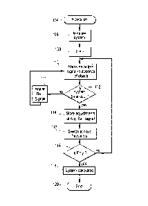
Fig. Ila is a flowchart showing the sequence of steps to calibrate the balance
of the detector
coil system according to an embodiment of the present invention;
Fig. 1lb is a flowchart showing the sequence of steps used to compensate the
output signal of
the detection coils for any noise according to an embodiment of the present
invention;
Fig. 12 is a circuit diagram of a portion of the detection circuitry according
to an
embodiment of the present invention.
CA 2859084 2017-07-255
5b
Fig. 13a is a vector diagram depicting the phase relationship between the
output signal as a
result of the interaction of ferrite.
Fig. 13b is a vector diagram depicting the phase relationship between the
output signal as a
result of the interaction of a product containing a metal contaminant with a
"clean" product.
Fig. 14 is a flowchart showing the sequence of steps to calibrate the detector
coil system
according to a particular product type.
Fig. 15 is a flowchart showing the sequence of steps in the testing of
products for metal
contamination according to an embodiment of the present invention.
In the case where the sensitivity of the metal detector is set very high so as
to detect very
small disturbances in magnetic field associated with small metal particles,
under certain
circumstances an out of balance in the detection coils can have a profound
effect on the
operation of the detection circuitry such as the detection coil amplifiers and
phase sensitive
detectors, which only operate over a limited voltage signal range. When the
detection coils
are in an imbalanced state there is a greater likelihood that the output
signal from moist
products as a result of the "product effect" will saturate the detection
circuitry at a given
operational frequency. For example, this can be illustrated in Fig. 3 with
reference to a
sinusoidal wave 8 having a peak-to-peak value in excess of the saturation
limit of +/-12v of
the detection circuitry. In an ideal situation, the output signal should read
zero if the system
is in a perfectly balanced state or below a predetermined threshold value.
However, when
the detection coil system is in a largely imbalanced state to the extent that
the output signal
occupies a significant portion of the operational range of the detection
circuitry, any
additional disturbance in the magnetic field as a result of the product effect
would greatly
increase the output signal beyond the saturation limit of the detection
circuitry. This is
schematically demonstrated in Fig. 3 showing the tops 14 (shown as dashed
lines) of the
output signal being "lost". To bring the output signal into range, the drive
signal is turned
down, thereby reducing the strength of the magnetic field between the
detection coils but
this is at the expense of reduced sensitivity of the metal detector. Thus,
there is the risk that
metal particles, particularly small metal particles would to be undetected as
the disturbance
CA 2859084 2017-07-25i
5c
in the magnetic field to be picked up by the detection circuitry would only be
very slight.
Moreover, the saturation of the detection circuitry may result in the detector
not recognising
a component of the output signal associated with a particular metal
contaminant being out of
phase with the component of the output signal associated with the product and
therefore,
likely to be ignored as discussed above.
CA 2859084 2017-07-255
6
In an attempt to mitigate such detection inaccuracies, the detection coil is
re-balanced at
each given operational frequency of the detector so bringing the balance
signal closer to the
zero line and thereby reducing the possibility that the detection circuitry
would saturate.
With reference to Fig. 3, this has the effect of increasing the "headroom"
signal 16
representing the distance from the peak of the balance signal to the
saturation limit of the
detection circuitry for detection purposes. Typically a mechanical balance is
employed to
balance the detection coils. Fig. 4 shows a schematic arrangement of the coil
configuration
18 embodying a mechanical balance 20 in the form of a coil or loop connected
between the
receiver coils, 22 and 24. The receiver coils 22, 24 are shown connected in
series. The
mechanical balance 20 provides some slack to the receiver coils 22 and 24 in
order to enable
their effective distance from the transmitter coil 26 to be adjusted which in
turn causes
changes to their magnetic field. One of the criteria for balancing the coil
system 18 is that
the effective distance of each of the receiver coils 22 and 24 from the
transmitter coil 26 is
identical. Since the physical properties of the receiver coils such as the
shape, size and the
number of windings are identical, by varying the relative distances from one
another of the
coil within the system 18, the output signal can be finely adjusted. The
detector is balanced
by manually manipulating the mechanical balance 20 usually by hand or a
specialist tool to
cause the effective distance of one of the receiver coils 22 and/or 24 to be
adjusted. Once
adjusted, the mechanical balance 20 is then encapsulated in a resin to prevent
any further
movement through physical shocks or handling of the metal detector. The
mechanical
balance 20 shown in Fig. 4 provides fine adjustments to the balance at a given
frequency.
For crude adjustments to the balance and in combination or separate to the
loop or coil 20,
an alternative mechanical balance can be provided. This involves placing a
block of metal of
a predetermined size in the vicinity of the coil system to cause deliberate
interference in the
magnetic field. By adjusting the position of the metal block between or around
the receiver
coils 22 and 24, the balance of the detection coil system can thereby be
adjusted. Even
though the mechanical balance once calibrated is thereafter encapsulated in
resin to prevent
any further movement, the method of calibration is prone to error. Any slight
movement of
the mechanical balance out of balance during the setting of the resin, would
mean that the
resin or seal has to be broken again and re-done. Moreover, this balancing
technique only
a-CA 28590842017-07-25
CA 02859084 2014-06-11
WO 2013/119741 PCT/US2013/025040
7
provides balancing of the coils at one frequency. To balance the detection
coils at the other
frequencies, would mean repeatedly manipulating the detection coils to cater
for the other
frequencies.
In contrast to a tuned circuit, modern metal detectors, as that taught in WO
2006/087510
(Spectrum Inspection Systems Ltd), operate over a large range of frequencies,
e.g. 40kHz to
900kHz. The time, effort and expense to re-set the balance mechanically at
each successive
frequency can sometimes be excessive and in some cases the result is not very
accurate.
Moreover, in a majority of cases the mechanical balance is permanently set in
resin, making
it impossible to re-set the balance mechanically. As a result only a few
select frequencies
are chosen for balancing, e.g. usually one at each extremity of the frequency
range and one
in the middle. Fig. 5 shows an exemplified distribution of the output signal
10 of a metal
detector throughout the operational frequency range of the detector with no
product to be
tested or contaminant present. Although, the detection coils are effectively
balanced at the
selected frequencies, A, B and C (see Fig. 5), this is not the case of the
output signal 10
from the detection coils outside of the selected frequencies resulting in a
non-zero output
signal. Thus, where a frequency is used for the detection of a particular
metal type that falls
outside of the selected frequencies, A, B and C there is a risk that the
detection circuitry will
saturate with consequential effects as discussed above.
WO 02/25318 (Safeline Limited) touches upon an automatic balance technique
whereby,
when the coils are out of balance, the out of balance signal determined by a
digital signal
processor causes a synthesiser to generate a corrective signal for subtraction
from the coil
output signal to cancel out the balance signal. No further detail is provided
how this is
achieved since it is necessary that phase and magnitude of the outbalance
signal is correctly
determined each time the output signal is out of balance in order to provide
the necessary
corrective signal. More importantly, the automatic balance only caters for
signals of a
sinusoidal nature derived from a tuned circuit and therefore, not geared for
variable
frequency metal detectors as taught in WO 2006/087510 (Spectrum Inspection
Systems
Limited).
As discussed above with reference to the vector diagram shown in Fig. 1, the
detection coil
system produces two signals, known as the resistive and reactive signals,
which tell the
CA 02859084 2014-06-11
WO 2013/119741 PCT/US2013/025040
8
detector about the interaction of the product with the magnetic field.
Conductive products
such as copper or stainless will generate an output signal having largely a
resistive
component. On the other hand, due to losses in the material, the component of
the output
signal from a poor conductor but perfect or near perfect magnetic material
will substantially
be in phase quadrature with the resistive signal. The differing output signals
from the
receiver coils will vary depending upon how conductive the product is. For
instance,
different types of products will interact differently with the magnetic field,
each product
having a resistive component and a reactive component and therefore, a
characteristic phase
angle.
When a perfectly magnetic material is passed between the receiver coils, one
would expect a
relatively weak or no resistive component indicating a weak conductive
material component
and a strong reactive component indicating a strong magnetic material. In
reality, this is not
exactly the case and a perfectly magnetic material exhibits both a reactive
component and a
notable resistive component resulting in a slight shift in phase angle from
the drive signal.
This shift in phase angle can be attributed to the delay in monitoring or
recording or
processing the output signal from the receiver coils. During the interaction
of the product
with the magnetic field between the receiver coils, there is a slight delay in
the system
picking up the signal. In circumstances where the product is a dry product (no
electrical
conductivity), such as a hard frozen product, a small phase angle is
generated. This delay
could be due to the interaction of the changing magnetic field with the
receiver coils and the
subsequent detection of the signal in the receiver coils as a result of the
electronics in the
detectors (e.g. phase sensitive detectors). This delay is usually
characteristic of a particular
metal detector and is traditionally calibrated by tuning the metal detector to
compensate out
or discriminate signals representing the resistive component and favouring
signals 900 to
this signal representing the reactive component in the presence of a ferrite
wand between the
detection coils Without compensating for this delay in the output signal,
products such as
dry products which exhibit little or no electrical conductivity may result in
a notable signal
being detected by the detection circuitry.
For a simple metal detector whereby the drive coil is driven by a tuning
circuit operating
over a limited range of frequencies, to calibrate for this delay and noise,
the ferrite wand is
passed between the detection coils at a given operating frequency, and the
generated output
CA 02859084 2014-06-11
WO 2013/119741 PCT/US2013/025040
9
signal is noted. Any discrepancy in the output signal, as a result of the
interaction of the
magnetic field with the ferrite, appropriate capacitors are then added to the
tuning circuit to
discriminate the output signal in the resistive phase. The time and effort to
manually add
capacitors to the tuning circuit to compensate for this delay factor, can be
cumbersome and
is prone to mistakes. Moreover, the whole manual correction of this delay
would need to be
repeated at the different operating frequencies. In the case of a variable
frequency metal
detector operating over a large range of frequencies, a lot of time and effort
would be
needed to calibrate for this delay factor at every operating frequency.
Moreover, the detection coils are very sensitive such that a signal is
generated from any
external influence such as a slight movement or vibration of the coils or the
presence of any
foreign metallic objects nearby the coils resulting in an undesirable noise
being generated
from the detection coils. When calibrating the metal detector for dry products
(no electrical
conductivity), such as hard frozen products (around -18 C), without any form
of calibration
of this noise, the metal detector will be confused as to whether the noise is
responsible of
the interaction of the dry product with the magnetic field or whether it' s
just background
noise. To compensate for this noise, a ferrite wand is passed between the
detection coils as it
produces a signal that closely resembles moving metal, i.e. similar to the
noise signal. By
compensating out or discriminating signals from a ferrite wand, the metal
detector becomes
very stable to vibrational noises. As the nature of the noise varies with
frequency, to
compensate for this noise at the different operational frequencies of the
metal detector
necessitates manually tuning the tuning circuit by adding appropriate
capacitors at the
different operating frequencies so as to discriminate signals from a ferrite
wand.
A system is thus required that:-
a) automatically balances the detector coil system throughout a range of
operational
frequencies irrespective of the shape of the signal, e.g. whether sinusoidal
or not, so
as to account for any imbalance in the detector coil system without the need
to
mechanically adjust the coils, and which ensures an adequately small or zero
output
signal in the absence of product and/or contaminants across a wide frequency
range;
b) automatically compensates for any delays or noise as a result of external
influences
in measuring the output signal without any or minimal manual intervention.
CA 2859084 2017-03-23
Summary of Invention
The present applicant has mitigated the above problems by providing an
adjustable balance
signal to counteract any imbalance in the coil system. More particularly, the
present
applicant provides a method of operation of a variable frequency metal
detector having a
5 driver circuit for establishing an alternating magnetic field in the coil
system so as to generate
an output signal at a given frequency; said driver circuit comprises a
plurality of switches
being arranged to cause the coil system to be driven at a frequency determined
by the
operation of the plurality switches, the method comprising the steps of:
a. generating an adjustable balance signal;
10 b. combining the adjustable balance signal with the output of the
detector;
c. adjusting the adjustable balance signal so as to provide a
compensated signal
whereby the output signal and/or the adjustable balance signal is filtered to
remove one or
more harmonics.
The invention in one broad aspect, pertains to a method of balancing an output
signal
of a variable frequency metal detector, the variable frequency metal detector
comprising a
driver circuit for establishing an alternating magnetic field in a coil system
so as to generate
an output signal at a given frequency. The driver circuit comprises a
plurality of switches
being arranged to cause the coil system to be driven at a frequency determined
by the
operation of the plurality switches. The method is characterized by the steps
of:
a. generating an adjustable balance signal;
b. combining the adjustable balance signal with the output signal of the
detector;
and
c. varying the adjustable balance signal so as to provide a compensated
signal,
whereby the output signal and the adjustable balance signal are filtered to
remove one or
more harmonics.
CA 2859084 2017-03-23
10a
Another aspect of the invention pertains to a method for scanning a product to
detect metal
on, in or associated with that product using a metal detector having a driver
circuit for
establishing an alternating magnetic field at a given operational frequency in
a coil system
so as to generate an output signal as defined in the method above, further
comprising the
steps
of:
a. selecting a desired operational frequency in the absence of the product;
b. retrieving the adjustments made to the adjustable balance at the desired
frequency stored in a database or look-up table.
c. adjusting the adjustable balance signal to the adjustments stored in the
database; and
d. compensating the output signal for the adjustable balance signal to
provide the
compensated signal.
Still further, the invention comprehends a metal detector for carrying the
method steps as
defined in the method set forth above, comprising:
a. a coil system;
b. a driver circuit for establishing an alternating magnetic field in the
coil system
to generate an output signal and an adjustable balance signal in the absence
of an product at
a given frequency;
c. an adjustor for varying the adjustable balance signal at the given
frequency
so as to combine with the output signal of the detector to provide a
compensated signal
wherein the metal detector further comprises a low pass filter to filter one
or more harmonics
from the output signal and the adjustable balance signal.
CA 2859084 2017-03-23
1 Ob
Generating an adjustable balance signal to combine with the output signal of
the detector coil
system, enables any imbalance in the system to be counteracted. Any signal
generating device
(driver) can be used to generate and vary an adjustable balance signal.
Examples, include a
digital oscillator, a synthesiser, an Electronic Programmable Logic Device
(EPLD) or even
a signal derived from the clock speed of a Central processing Unit. More
particularly, the
adjustable balance signal can be varied to an extent so that when combined
with the output
of the detector it nullifies the output signal. The adjustable balance signal
is injected or bled
from a driver signal used to drive the drive coil (drive signal) to combine
with the output
signal. Preferably, the driver circuit generates a drive signal for
establishing an alternating
magnet field in the coil system and the adjustable balance signal is derived
from the drive
signal. For example, the signal to drive the drive coil can be based on an
internal clock
oscillator of the EPLD which is used to generate a varying signal of a given
frequency to
control a plurality of switches, e.g., Field Effect Transistors (FET) in a
driver circuit as
taught in WO 2006/087510 (Spectrum Inspection Systems Limited). Typically, an
EPLD
comprises one or more drive maps stored in the EPLD a CPU coupled to the EPLD
selects
a drive map which then controls the internal clock oscillator to send
appropriate signals to
a driver to repeatedly control the operation of a plurality of switches to
generate a signal of
a given frequency. Alternatively, the drive maps for driving the EPLD can
equally be stored
in the CPU. As the adjustable balance signal is derived from the drive signal,
the
CA 02859084 2014-06-11
WO 2013/119741 PCT/US2013/025040
11
adjustable balance signal will be at the same frequency as the drive signal
but with a fixed
phase relationship. In terms of the total output signal, by nullifying any
imbalance in the
output signal and in absence of any products between the coil system or for
'dry products',
i.e. products that do not generate a signal in the coil system, reserves a
greater portion of the
output signal or "headroom" signal for detection of contaminants without
saturating the
detection coil amplifiers. Ideally maximum range or "headroom" signal for the
detection of
contaminants is provided by effectively nullifying any imbalance in the coil
system. This in
turn permits the drive signal to be "turned-up" (i.e. increase the voltage
supplied to the drive
coil) so increasing the sensitivity of the metal detector to detect small
variances in the output
signal without saturating the detection circuitry.
Preferably, the compensated signal is measured and if the compensated signal
is above a
predetermined threshold value, repeat step(c) above so that when combined with
the output
signal of the detector, the compensated signal is below a predetermined
threshold value.
Preferably, the predetermined threshold value is equal to substantially zero
for a perfectly
balanced system but can be any value chosen so as to give a balanced coil
system, e.g.
sufficiently balanced for useful contaminant detection. Typically, a metal
detector has a
detection range beyond which the metal detector, more particularly the
detection circuitry,
will saturate. Ideally, the predetermined threshold value is less than
substantially 40% of the
detection range of the detection circuitry, preferably less than substantially
15% of the
detection range of the detection circuitry, more preferably less than
substantially 10% of the
detection range of the detection circuitry. Thus for a given frequency, where
there is an
imbalance in the coil system resulting in a non-zero output signal or outside
the permitted
range in the absence of any product or contaminant or for dry products, the
system
automatically varies the adjustable balance signal so that the adjustable
balance signal
combines with the output of the detector to compensate for this non-zero
output to bring it
into balance, e.g. resulting in a substantially zero signal or below a
predetermined threshold
value. This could be done through a trial and error process, e.g. varying the
adjustable
balance signal incrementally and for each incremental step, the output signal
is measured to
see if it is below a permitted range. Once the output signal is below a
permitted range, the
adjustment made to the adjustable balance signal is stored. For example, a
detection
circuitry operating at a peak-to-peak detection range of +/-12 volts, then the
permitted
predetermined threshold value to establish balancing of the metal detector in
the absence of
CA 02859084 2014-06-11
WO 2013/119741 PCT/US2013/025040
12
products ill the detection coils would result in an output voltage of less
than substantially 4.8
volts, preferably less than substantially 1.8 volts, more preferably less than
substantially 1.2
volts.
Optionally, the adjustable balance signal at a given frequency is combined
with the output
of the detector coil system by superimposing the adjustable balance signal on
the output
signal. More preferably, the method of compensating the output signal with the
adjustable
balance signal can involve calculating the difference between the adjustable
balance signal
and the output signal, e.g. magnitude and phase. To balance the coil system,
the phase and
amplitude of the adjustable balance signal are varied so that when subtracted
from the
output signal substantially nullifies the output signal. This can be
represented graphically by
the vector diagram in Fig. 1. An imbalance in the output signal is shown by
the vector Vout
having a phase component and an amplitude determined by the length of the
vector. To
nullify the output signal, Vout, the adjustable balance signal VABS is varied
so that its phase
component and amplitude are substantially equal and opposite of the output
signal. This is
represented graphically by additionally providing a vector component VABS
having a phase
and magnitude that is substantially equal and opposite to the vector, Vout.
This is
effectively nullifying the output signal. However, the adjustable balance
signal, VABS can
be varied to effectively reduce the output signal to below a predetermined
compensated
value. The type and nature of the adjustable balance signal will depend on the
nature of the
output signal. The simplest approach is where the output signal is sinusoidal
in nature, e.g.
derived from a tuned circuit and thus, the balancing signal is one selected to
substantially
cancel the sinusoidal wave. Where the drive signal is derived by a plurality
of switches as
found in a variable frequency metal detector, the output signal is in an
uncontrolled shape
and therefore, lacks any symmetry, i.e. more specifically the output signal
adopts a more
square or trapezoidal shape with one or more harmonics. Thus, establishing an
adjustable
balance signal to nullify or reduce the imbalance in the output signal is more
complicated
than where the output signal is sinusoidal in nature. Simply establishing an
equal and
opposite signal to cancel the output signal is not always appropriate in this
case. The
adjustable balance is varied to an extent that when combined with the
imbalanced signal
effectively reduces the signal to below a predetermined threshold value or
nullify the output
signal. The algorithms to achieve this can be more complicated than simply
adding or
subtracting the signals, as one would expect from a signal from a traditional
tuning circuit.
CA 02859084 2014-06-11
WO 2013/119741 PCT/US2013/025040
13
What is important in the present invention is that the resultant output from
the combined
adjustable balance signal and the imbalanced signal reaches below a
predetermined
threshold value.
Preferably, the adjustable balance signal is based on the drive signal having
a phase and
amplitude component that is adjusted so that it is substantially equal and
opposite to the
output signal. Preferably, at a given operational frequency of the metal
detector, the
adjustable balance signal is varied by increasing or decreasing the adjustable
balance signal
in sequential steps. At each step, the output signal is measured to see if it
has reached below
a predetermined threshold value. If not, the adjustable balance is incremented
and the
measuring process repeats to see if it has reached below a predetermined
threshold value.
Once the output signal reaches below a predetermined threshold value, the
adjustments
made to the adjustable balance signal at a given frequency are stored in a
database or look-
up table for later retrieval at that given frequency. By varying the
adjustable balance signal
through a trial and error process help to mitigate the complications in
mathematically
establishing a cancelling signal for any imbalance in the output signal.
Preferably, the process of calibrating the metal detector by nullifying the
output signal or
balancing the coil system is repeated for successive frequencies. Preferably,
the frequency is
varied incrementally, more preferably in substantially 10Hz increments. This
is made
possible since the process of balancing the coil system is automated. More
preferably, the
adjustable balance signal can be varied by software. Whereas in prior art
metal detectors
only a select few frequencies are subjected to the balancing process due to
the time and
effort to physically adjust the separation of the coils to compensate for the
level of
imbalance, controlling and varying the adjustable balance signal through the
use of
software to quantitatively measure the level of imbalance of the coil system
and
automatically configure the drive signal to bring it into balance automates
the balancing
process and thereby a greater range of operational frequencies can be
subjected to the
balancing process.
Preferably, the adjustable balance signal is varied by a potentiometer, more
preferably a
digital potentiometer. The use of a digital potentiometer enables the
adjustable balance
signal to be controlled by software. This allows the system to automatically
nullify any
CA 02859084 2014-06-11
WO 2013/119741 PCT/US2013/025040
14
imbalance in the system, i.e. compensate the output of the coil system by the
adjustable
balance signal to provide a compensated signal. The use of one or more
potentiometers
allows the balancing signal to effectively compensate for any imbalance in the
output signal
irrespective of the shape or form of the output signal. This is even possible
where the coil
system is driven by a plurality of switches as taught in WO 2006/087510
(Spectrum
Inspection Systems Limited), where the resulting square wave (or a trapezoidal
wave)
generates a large number of relatively high energy harmonics compared with the
conventional sinusoidal signal generated by a tuned circuit. Preferably, the
potentiometer
comprises a first potentiometer and a second potentiometer and the adjustable
balance
comprises a first adjustable balance signal and a second adjustable balance
signal. The first
adjustable balance signal is varied by the first potentiometer and the second
adjustable
balance is varied by the second potentiometer. Preferably, the first
adjustable balance signal
is substantially not in phase with the second adjustable balance signal. More
preferably, the
first adjustable balance signal is out of phase with the second adjustable
balance signal by
equal to or less than substantially 90 . It has been found that the further
apart the first and
second adjustable balance signals from 90 , the more difficult it would be for
the adjustable
balance signals to balance any imbalance in the output signal. Preferably, the
first adjustable
balance signal is in phase with the drive signal and the second adjustable
balance signal is
not in phase with the drive signal. Preferably, the second adjustable balance
signal is out of
phase with the drive signal by substantially 90 . Equally, the first
adjustable balance signal
and/or the second adjustable balance can be set at any arbitrary angle that is
not in phase
with the drive signal or not in phase quadrature (90 out of phase with the
drive signal) with
the drive signal respectively. Varying the balance signal by two
potentiometers allows the
full 360 phase angle of the output signal to be covered. Optionally, the
adjustable balance
signal can be varied by a tuning circuit comprising a variable resistor
(potentiometer), a
variable capacitor and/or a variable inductor. In contrast to two
potentiometers, a tuning
circuit comprising a potentiometer, a variable capacitor and/or inductor only
allows 90
phase angle variation of the drive signal to be covered.
More preferably, the adjustable balance signal is varied by an Electronic
Programmable
Logic Device (EPLD), e.g. a Complex Programmable logic device (CPLD) or Field
Programmable Gate Array (FPGA). Coupled to an EPLD. a CPU selects a drive map
stored
in the EPLD or in the CPU which then sends signals to a driver to generate
both drive
CA 02859084 2014-06-11
WO 2013/119741 PCT/US2013/025040
signal and adjustable balance signal at a given working frequency. For
example, the driver
comprises a plurality of switches, e,.g. FETs, such that through a selection
of the drive map
stored in the EPLD, the EPLD controls an internal clock oscillator to drive a
plurality of
switches, e.g. FETs, to create the transmitter drive signal at a given
frequency. As the
5 adjustable balance signal is derived from the drive signal, the
adjustable balance signal will
be at the same frequency as the drive signal. In addition for generating the
drive signal and
the adjustable balance at a given working frequency, the CPU coupled to the
EPLD can also
be used to vary the amplitude and phase of the generated adjustable balance
signal. This
removes the need for a potentiometer or tuning circuit as the variation in the
adjustable
10 balance signal can be done purely through use of programmable logic
circuits (PLCs).
The adjustable balance signal in step (a) and/or the combined adjustable
balance signal
and/or the output signal in step (b) above is filtered by a low pass filter,
more preferably a
switchable low pass filter to cater for the different operating frequencies.
Whereas in known
15 auto-balance systems, the system is based on a regular sinusoidal wave
generated over a
limited range of frequencies by means of a tuning circuit, the output from a
variable
frequency metal detector whereby the drive coil is driven by a plurality of
switches,
generates a square wave (or trapezoidal wave) with a large number of high
energy
harmonics or harmonic distortions along with the fundamental frequency of
operation, i.e.
the resultant wave typically has an uncontrolled shape. In absence of the low
pass filter, the
detector runs the risk that the peak signal voltage of the compensated signal
as a result of the
harmonics may exceed the predetermined threshold value of the compensated
signal
resulting in a continuous imbalance. More importantly, the peak signal voltage
may exceed
the saturation limit of the detection circuitry. The low pass filter filters
out one or more
harmonics from the adjustable balance signal and/or the output signal leaving
the
fundamental component, i.e. generates a more sinusoidal waveform that is more
workable
and measurable and is not disrupted by the high energy harmonics.
The adjustable balance signal and/or the output signal can each individually
be filtered by
one or more low pass filters to remove one or more harmonics from their
respective signals
prior to being combined to form the compensated signal. The low pass filter
also allows the
adjustable balance signal to be effectively varied by the potentiometer or PLC
or otherwise
so as to compensate for any imbalance in the output signal irrespective of
their shape or
CA 02859084 2014-06-11
WO 2013/119741 PCT/US2013/025040
16
wavefon-n or the presence of any harmonic distortion. This simplifies the
'balancing'
operation, because less steps are needed to reach a balanced state since the
signal has a
waveform that is more "manageable" (generates a more sinusoidal waveform) than
a signal
with a waveform having no regular shape.
During an initial start-up of the metal detector, the system scans through a
range of
operating frequencies and varies the adjustable balance signal by
automatically adjusting the
potentiometer at each given frequency necessary to balance the detection coil
system. A
database or look-up table is built up of stored adjustments of the
potentiometer for different
operating frequencies. A time delay can be provided before each measurement of
the
baseline signal in order to allow the frequency of the detection coil system
to stabilise.
Preferably, the operating method for detecting metal contaminants comprises
the step of:
a) selecting a desired frequency of operation in the absence of an object;
b) retrieving the stored adjustments made to the adjustable balance signal at
the desired
frequency from the database;
c) adjusting the adjustable balance signal to the adjustments in the database;
d) compensating the output signal for the adjustable balance single to provide
the
compensated signal.
The above process pertains to the product calibration stage whereby the metal
detector,
more specifically the coil system, is calibrated for a particular product type
and involves
selecting an operational working frequency for that product type so that the
output signal
from any metal contaminants embedded in the product can easily be
distinguished from the
output signal from the product alone. In absence of any products in the
detector or for dry
products, combining the adjustable balance signal with the output signal as a
result of any
imbalance in the coil system will result in the compensated signal, e.g.
nullify the imbalance
in the coil system. Once a desired frequency of operation is selected based on
the
characteristics of the product such as size, electrical conductivity, magnetic
permeability,
combining the adjustable balance signal with the output signal of the detector
optionally
comprises the step of subtracting the adjustable balance signal from the
output signal. As
discussed above, since the output signal is in an uncontrolled shape and
therefore, lacks any
symmetry, merely detecting whether the combined adjustable balance signal and
the output
CA 02859084 2014-06-11
WO 2013/119741 PCT/US2013/025040
17
signal reaches below a predeten-nined threshold value is normally required. In
operation,
the operator manually selects a desired frequency of operation through
experience of the
product type. Once the frequency of operation has been selected, the system
searches the
database to retrieve the stored adjustment of the potentiometer, PLC etc., at
that
corresponding operating frequency from the earlier signal balancing
calibration stage
described above. If the system realises that at the particular operating
frequency, there is an
imbalance in the detection coil system resulting in a residual or non-zero
baseline signal, the
system compensates the output signal by combining with the appropriate
nullifying
adjustable balance signal to provide a more accurate representation of the
output signal.
This prevents the imbalance in the detection coil system from affecting the
measured output
signal.
The product calibration stage further comprises the steps of passing a test
product through
the detector, measuring the output signal as a result of the interaction of
the test product
with the magnetic field between the detection coils and then storing the
measured output
signal. A test product is a product that is representative of the product
under investigation
with no known contaminant present. This is to provide a base signal for the
product type
such that any variance in the output signal, e.g. phase angle, from future
similar products
under investigation from this base signal is an indication of a metal
contaminant. This is
because a contaminant will interact differently with the magnetic field
resulting in an output
signal having a different phase angle from that of the product alone.
Typically, similar
products under investigation are placed on a conveyor belt and the output
signal is measured
and compared with the stored output signal (base signal) from the test product
at that
operational frequency to see if there is any variance from the base signal.
For example,
consider the signal derived from the drive signal to have a P component that
is
representative of the in-phase component of the drive signal and a Q-component
that is
representative of the phase quadrature component of the drive signal. In the
particular
embodiment described below, the P' and Q' components of the output signal are
measured.
The P' component represents the in-phase component of the output signal and
the Q'
component represents the quadrature component of the output signal. This
should not be
mistaken for a P component and Q component of the signal derived from the
drive
signal,discussed above. For example, the adjustable balance signal derived
from the drive
signal has a P component that is in phase with the drive signal and a Q
component that is in
CA 02859084 2014-06-11
WO 2013/119741 PCT/US2013/025040
18
phase quadrature with the drive signal. The phase angle of the output signal
is determined
from the measured P' and Q. values, e.g. by means of simple trigonometry.
Further detail of
the product calibration stage is described in the specific embodiment below.
The invention correspondingly provides a metal detector comprising a) coil
system; b) a
driver circuit for establishing an alternating magnetic field in the coil
system so as to
generate an output signal and an adjustable balance signal in the absence of
an object at a
given frequency and c) an adjustor for varying the adjustable balance signal
at said given
frequency so as to combine with the output of the detector to provide a
compensated signal.
Preferably, the driver circuit is arranged to operate the coil system at any
one of a selection
of different frequencies. The sensitivity of a metal detector is determined by
the ability of
the metal detector to select an optimum frequency of operation for a
particular product type.
For example, whereas one product is detectable at one particular frequency,
this is not the
case at another frequency or for another product type. Moreover, whereas at
one frequency a
food product is successfully discriminated from a metal contaminant, this is
not the case at
another frequency. Thus for a given product type, the metal detector has to be
able to switch
through a range of frequencies in order to provide an optimum sensitivity of
operation. The
driver circuit comprises a plurality of switches being arranged to
alternatively connect the
coil system across a potential difference to cause the coil system to be
driven at an operating
frequency determined by the operation of the switches as described in the
international
patent application WO 2006/087510 (Spectrum Inspection Systems Ltd).
Preferably, the
plurality of switches can be field effect transistors (FETs) as taught in WO
2006/087510
(Spectrum Inspection Systems Ltd), bipolar junction transistors (BITs) or any
other suitable
switching device. By controlling the input to the coil system using a
plurality of switches,
instead of the conventional tuned circuit, it is possible to program a
processor or
programmable controller to operate the plurality of switches so that any
desired frequency
of operation can be obtained in order to maximise the sensitivity of the metal
detector. For
example, as discussed in WO 2006/087510 (Spectrum Inspection Systems Ltd), the
CPU
monitors to see whether the detection coils are saturated or a metal
contaminant is
successfully discriminated in a test sample and in response to this, selects
an appropriate
frequency of operation. This would enable the metal detector to simply be
installed and
switched on, the metal detector monitoring its own operation and selecting an
appropriate
CA 02859084 2014-06-11
WO 2013/119741 PCT/US2013/025040
19
drive frequency for a particular product type. This would also permit
different product types
to be used with a detector, with the detector recognising when it is necessary
to select a
different frequency. Typically and as described above, during operation of a
metal detector
an operator will normally manually select a desired frequency of operation for
a particular
product type through experience. The driving of the coil system by means of a
plurality of
switches permits the operator to select an ideal frequency of operation from a
greater range
than traditionally using tuned circuits.
Preferably, the driver circuit comprises a microprocessor (CPU) and an
electronically
programmable logic device, the output of the electronically programmable logic
device
controls said switches, wherein for a particular detection coil, a plurality
of drive maps is
stored in the electronically programmable logic device each containing a
switching
sequence for the switches for a respective predetermined frequency of
operation of the coil
system, wherein the microprocessor selects an appropriate switching sequence
depending on
the selected frequency of operation. This provides a convenient way of
ensuring the
switches are controlled in a precise and predetermined manner for any
frequency selected.
Preferably, the metal detector of the present invention comprises a
microprocessor and an
electronically programmable logic device for varying the adjustable balance
signal at a
given frequency and combining said adjustable balance signal with the output
signal at said
given frequency of the drive signal to provide a compensated signal. The
electronically
programmable logic device for varying the adjustable balance signal can be the
same
electronically programmable logic device as used for driving the coil system
as discussed
above. More sophisticated electronically programmable logic devices such as
Complex
Programmable logic device (CPLD) or Field Programmable Gate Array (FPGA) allow
more
complex operations to be performed. More preferably, the microprocessor is
built into the
metal detector. Alternatively, the microprocessor is provided by a personal
computer.
Preferably, the metal detector comprises a storage device for storing the
adjustments made
to the adjustable balance signal to provide the compensated signal. For
example, take the
example where the adjustable balance signal is varied by one or more
potentiometers, then
at each operating frequency the microprocessor stores the adjustments made to
the
potentiometer necessary to balance the detector coil system. A database or
look-up table is
CA 02859084 2014-06-11
WO 2013/119741 PCT/US2013/025040
thus built up showing the adjustments of the potentiometer and/or compensated
signal for
each corresponding operating frequency.
Preferably, the coil system comprises a drive coil and a detection coil so
that in use when an
5 alternating magnetic field is established in the coil system, the
detection coil inductively
couples with the magnetic field associated with the drive coil to generate an
output signal.
More preferably, the detection coil comprises at least a first and second
detection coil at
separate locations and arranged such that the presence of a metal will distort
the magnetic
field associated with the drive coil and produce an imbalance in the output of
the detection
10 coils resulting in a substantially non-zero output from the detection
coils. The first and
second detection coils are preferably arranged substantially in opposition and
are electrically
connected in series or parallel. By connecting the first and second detection
coils in
opposition, their induced voltages oppose one another and thereby cancel. If
the coil system
is in a perfectly balanced state their output signal is zero. In contrast,
where the coil system
15 is in an imbalanced state their output signal is substantially non-zero.
In addition to or in combination to calibrating the output signal to
compensate for any
imbalance in the output signal, in a second embodiment of the present
invention the system
preferably compensates for noise as a result of the delays in the interaction
of the magnetic
20 field with the product under investigation and the detection electronics
and noise from
moving metal. The present applicant has mitigated the above problems by
providing a
system that automatically compensates the output signal to take into account
noise derived
from delays through the interaction of the magnetic field with the product
under
investigation and the detection electronics and/or noise as a result of
external influences
disrupting the measurements in the detection coils, e.g. vibration. This noise
is usually
measured by recording the interaction of the magnetic field in the coil system
with ferrite. In
theory, the output signal from ferrite resembles the output signal as a result
of noise. Thus
by discriminating or compensating out the output signal from ferrite, signals
responsible for
noise can effectively be reduced or substantially reduced, i.e. the metal
detector is
compensated for any external disturbances to the coils. Thus, the compensated
signal for
noise will represent a fixed reference point from which future measurements
are made. In
the present invention, the term "compensated out" or "discriminated" is where
the output
signal is reduced to a substantially zero value or a near zero value.
CA 02859084 2014-06-11
WO 2013/119741 PCT/US2013/025040
21
In addition to the noise as a result of external influences acting on the
coils, there is also
delays in measuring the output signal in the detection electronics as a result
of the
interaction of the product under investigation with the magnetic field and
subsequent
recordal of its output signal. Without compensating for this delay, the phase
angle of the
output signal from a product under investigation would lag behind or lead the
'true' output
signal if there were no delays in the detection electronics. Since the phase
angle of the
output signal is representative of the type of product or contaminant present
between the
coils, any delays in the phase angle results in wrongly identifying the type
of product under
investigation or contaminant. To cater for this delay, traditionally the phase
angle of any
product under investigation is measured with reference to a fixed reference
signal at a given
frequency. This reference signal is chosen so that a phase angle of zero
degrees represents a
product that is purely energy absorbing, e.g. a perfect or near perfect
magnetic material. In
theory, and everything being perfect, a perfect or near perfect magnetic
material due to the
interaction with the magnetic field should largely result in a reactive signal
that is in phase
quadrature with the resistive signal. However, due to this delay in the
detection electronics,
the output signal from a perfect magnetic material at a given frequency has a
quadrature
component but also a resistive component. Thus, if we consider the vector
diagram shown
in Fig. 1, the vector line corresponding to the output signal from a perfect
magnetic material
will lie between the resistive axis and the reactive axis. In view of this
discrepancy, the
output signal is adjusted so that the output signal from a perfect magnetic
material is largely
in the reactive region with minimal or no resistive component. The nearest
best thing to a
perfect magnetic material in the industry is ferrite material. Although not
purely magnetic,
the output signal from ferrite does provide a good reference point to tune the
metal detector
to favour an output signal in a given phase whilst eliminating those signals
in phase
quadrature to this direction. In fact, the output signal from fenite generates
an output signal
that is largely reactive and therefore, the resistive component would largely
be substantially
zero or compensated out.
The present invention provides a method of operation of a metal detector
wherein the output
signal is automatically compensated for any delays or noise in measuring the
output signal
at given frequency, said output signal having a first component and a second
component, the
first component being out of phase with respect to the second component at a
predetermined
CA 02859084 2014-06-11
WO 2013/119741 PCT/US2013/025040
22
phase angle, wherein the output signal is compensated for any noise or delays
in measuring
the output signal at a given frequency by the steps of:
a. measuring the output signal in the presence of ferrite between the coil
system,
b. digitally adjusting the output signal so that the output signal in the
first or second
component of the output signal is equal to or below a first predetermined
threshold value
and the output signal in the second or first component of the output signal is
equal to or
above a second predetermined threshold value,
c. storing the adjustments made to the output signal in a database or a
look-up table,
d. repeating steps a, b and c for different frequencies.
Preferably, the output signal is digitally adjusted so that the magnitude of
the output signal
in the first or second component of the output signal is equal to or below a
first
predetermined threshold value and the magnitude in the second or first
component of the
output signal is equal to or above a second predetermined threshold value. By
storing the
adjustments made to the output signal as a look-up table or database removes
the
requirement to manually adjust the output signal to compensate for this delay.
Preferably,
the look-up table or the database is separate to the look-up or database used
to calibrate for
any imbalance in the output signal as discussed above. As this delay is
usually characteristic
of a particular metal detector, providing for this calibration can be carried
out at the factory
site prior to being shipped out to the customer's site, i.e. on first
manufacture. By digitally
compensating this delay factor in the measurement of the output signal but
more importantly
by storing the adjustments made to the output signal removes the need of
repeatedly adding
capacitors to a traditional tuning circuit in order to adjust the output
signal so that in the
presence of ferrite, the output signal will largely be the reactive component.
Preferably, the first component of the output signal is substantially in phase
quadrature with
the second component of the output signal. As the reactive component is in
phase
quadrature with respect to the resistive component, by adjusting the output
signal having a
first component that is in phase quadrature with a second component, it is
possible to
discriminate or compensate out the output signal from ferrite in either the
first component or
the second component of the output signal, leaving largely the output signal
in the second or
first component of the output signal. The term "compensated out" or
"discriminated"
represents the situation whereby the output signal is adjusted so that it is
substantially zero
CA 02859084 2014-06-11
WO 2013/119741 PCT/US2013/025040
23
or near zero (a minimum predetermined threshold value) at one phase angle with
respect to
the drive signal and the output signal is dominated at another phase angle
with respect to the
drive signal. This situation occurs when the phase angle between the first and
second
component of the output signal is substantially equal to 900. When viewed on a
vector
diagram, the vector line representing the output signal is effectively rotated
so that it lies
substantially or nearby on the reactive axis having no or little resistive
component. In this
way, the output signal that is generated as a result of the interaction of
ferrite with the
magnetic field will largely be the reactive component. For example, setting
the metal
detector to detect a P' signal (first or second component) and a Q' signal
(second or first
component) whereby the P' component is in phase quadrature with the Q.
component, then
the metal detector is adjusted so that the output signal is largely the Q'
signal or the P'
signal, i.e. the reactive component, and little or no Q' or P' signal
(resistive component).
Thus, knowing that one of the components of the output signal from ferrite
should read zero
or near zero, the output signal is adjusted in the presence of ferrite at a
given frequency so
that it largely generates a reactive signal and a zero or near zero resistive
signal (one of the
components reads substantially zero and the output signal is dominated by its
phase
quadrature component). It is this relationship in measuring a maximum Q' or P'
value and a
minimum P' or Q' value in the presence of ferrite between the detection coils,
that allows
the system to compensate the system for any noise or delays in the detection
system.
However, this relationship in measuring the output signal is not restricted to
adjusting the
output signal so as to produce a substantially maximum first or second
component when the
second or first component of the output signal is substantially zero, i.e. at
the condition
where the first or second component is in phase quadrature with the second or
first
component of the output signal. The angle between the first and the second
component of
the output signal can be at any predetermined phase angle so as long as the
system can
identify a 'maximum and minimum' relationship between the two components of
the output
signal. Instead of adjusting the phase angle of the output signal from ferrite
such that one of
the components is substantially equal to zero (i.e. when the two components of
the output
signal are in phase quadrature), the output signal can be adjusted such that
the first or
second component of the output signal is equal to or below a first
predetermined threshold
value and the second or first component of the output signal is equal to or
above a second
predetermined threshold value. In this situation, the first component of the
output signal is
not in phase quadrature with the second component of the output signal but at
another
CA 02859084 2014-06-11
WO 2013/119741 PCT/US2013/025040
24
arbitrary phase angle. The first and second predetermined threshold value
being largely
determined by the phase angle between the first and second component of the
output signal.
Preferably, the output signal is digitally adjusted so as to discriminate the
output signal in
the first or second component of the output signal such that the output signal
in the first or
second component of the output signal is substantially equal to zero. By
compensating the
resistive component out, any noise in the detection electronics will also be
taken into
account. In order to compensate the output signal in the first or second
component of the
output signal, preferably the metal detector comprises a phase sensitive
detector, whereby
the output signal is compensated for any delays or noise in measuring the
output signal at a
given frequency by the steps of;-
a. generating a reference signal;
b. combining the reference signal with the output signal of ferrite in the
phase sensitive
detector at a given frequency
c. digitally adjusting the reference signal such that when combined with
the output
signal from ferrite, the output signal in the first or second component of the
output
signal is equal to or below a first predetermined threshold value and the
output
signal in the second or first component of the output signal is above a second
predetermined threshold value;
d. storing the adjustments made to the reference signal in a database or
look-up table;
e. repeating steps a, b, c and d at different frequencies.
By generating a reference signal based on the drive signal, the reference
signal can be
adjusted so that when combined with the output signal from ferrite in the
phase sensitive
detector, the output signal in the first or second component of the output
signal is equal to or
below a first predetermined threshold value and the output signal in the
second or first
component of the output signal is above a second predetermined threshold
value.
Preferably, digitally adjusting the reference signal so as to discriminate the
output signal in
the first component or the second component of the output signal, i.e.
substantially equal to
zero. The first and second predetermined threshold value being largely
determined by the
cosine of the angle between the reference signal and the output signal. Thus,
when the angle
between the reference signal and the output signal is equal to 90 , the phase
sensitive
CA 02859084 2014-06-11
WO 2013/119741 PCT/US2013/025040
detector compares the reference signal and the output signal to produce a
substantially zero
value (Cosine 900 = 0). Maximum value is obtained when the output signal is in
phase with
the reference signal (Cosine 00 = 1). Preferably, the metal detector comprises
a first and
second phase sensitive detector and the reference signal comprises a first
reference signal
5 and a second reference signal such that at a given frequency the first
reference signal is
combined with the output signal in the first phase sensitive detector to
produce a first
component of the output signal and the second reference signal is combined
with the output
signal in the second phase sensitive detector to produce a second component of
the output
signal. By varying the first and/or second reference signal, an adjustment is
reached
10 whereby the 'maximum and minimum' conditions of the output signal in the
presence of
ferrite are met. More specifically, when the first reference signal is in
phase quadrature with
the second reference signal, then the output signal in the first or second
component of the
output signal is compensated out or discriminated to largely read a zero or
near zero signal
and the output signal from ferrite will be dominated by either the output
signal in the second
15 or first component of the output signal that has not been compensated
out, i.e. the reactive
component. In other words, the output signal is effectively rotated so that it
lies substantially
or substantially superimposes on the reactive axis. Preferably, the reference
signal, more
specifically, the first and/or second reference signal, are increased
incrementally and the
output from the first and second phase sensitive detectors are monitored to
establish whether
20 the output signal in the first or second component of the output signal
is equal to or below a
first predetermined threshold value or has been compensated out, i.e. reads
substantially
zero. When the output signal in the first or second component has reached
below a
predetermined threshold value or has been compensated out, the output signal
in the second
or first component is above a second predetermined threshold value or has
reached a
25 maximum value. Preferably, the first reference signal is substantially
in phase quadrature
with the second reference signal to mimic the fact that the reactive signal is
substantially in
phase quadrature to the resistive signal, such that when combined with the
output signal in
the first and second phase sensitive detectors respectively, the first
component of the output
signal is substantially in phase quadrature with the second component of the
output signal.
By compensating out the output signal from ferrite in the first or second
component, results
in a signal that is purely reactive and therefore takes into account the
delays in the detection
electronics. Each time the output signal is compensated out/discriminated or
reached below
a first predetermined threshold value in the first or second component of the
output signal
CA 02859084 2014-06-11
WO 2013/119741 PCT/US2013/025040
26
(depending which component of the output signal is substantially in phase
quadrature with
the reference signal) at a given frequency, the adjustments made to the
reference signals at
that given frequency is stored in a database or look-up table for later
retrieval. This
represents the fixed reference point from which future products under
investigation are
measured. As the nature of the noise or the delays in the detection system
varies with
frequency, this is repeated at different operational frequencies of the metal
detector.
Preferably, the reference signal is digitally adjusted by incorporating a
delay factor in the
reference signal. Where the reference signal in based on the drive signal
generated by an
Electronically Programmable Logic Device (EPLD), then the adjustments can be
made by
incrementally adjusting the high speed counter or drift register of the EPLD.
In operation when scanning a product to detect metal on, in or associated with
that product,
the method preferably comprises the steps of:
a. retrieving the adjustments made to the output signal at a desired
operational
frequency of the metal detector from the database or look-up table;
b. adjusting the output signal to the adjustments stored in the database
or look-up table
so to compensate for any noise or delay in measuring the output signal.
During scanning a product under investigation to detect for metal
contamination at a given
operational frequency of the metal detector, the system (e.g. processor)
retrieves the
adjustments made to the output signal from the database or look-up table and
subsequently
adjusts the output signal to the adjustments stored in the database or look-up
table so as to
compensate for any delay in measuring the output signal. Preferably, the phase
and/or
magnitude of the output signal are compensated for the adjustments stored in
the database or
look-up table. Following compensation of the output signal, the measured
output signal in a
first or second component of the output signal as a result of the interaction
of the product
under investigation with the magnetic field will represent the -true" first or
second
component of the output signal that has been compensated for any noise or
delays.
Likewise, the measurement of the second or first component of the output
signal as a result
of the interaction of the product with the magnetic field represents the
"true" second or first
component of the output signal that has been compensated for any noise or
delays. Without
any form of compensation, the first or second component of the output signal
and the
27
second or first component of the output signal will either lead or lag behind
the "true" first
and/or second components of the output signal.
Each time the metal detector is used to test products under investigation at a
given
frequency, the metal detector, more particularly the processor, retrieves the
appropriate
correction factor from the look-up table and makes the appropriate corrections
to the output
signal, more specifically to the reference signal, to compensate for any
noises or delays in
the output signal. Preferably, the phase and/or magnitude of the output signal
are
compensated for the adjustments stored in the database or look-up table. More
specifically,
the output signal is calibrated to a fixed reference point so that any
measurements made
from products under investigation at a given frequency are made relative to
this fixed
reference point. Preferably, the adjustments to the output signal to
compensate for any noise
or delays in the output signal discussed in the second embodiment of the
present invention
can be used in conjunction with compensating for any imbalance in the output
signal as
discussed with the first embodiment of the present invention.
As discussed with the first embodiment of the present invention, the metal
detector can be a
variable frequency metal detector whereby the driver circuit comprises a
plurality of
switches arranged to cause the coil system to be driven at a frequency
determined by the
operation of the plurality of switches. As a variable frequency metal detector
operates over a
large frequency range, digitally compensating for any noise or delays in the
output signal
offer significant benefits over traditional metal detectors based on tuning
circuits both in
terms of efficiency and accuracy of measurement.
Preferably, the metal detector comprises a rectifier to convert the output
signal of the
detection coil to a direct current (DC), so that the signal can be digitized.
This enables the
output signal to be read by the microprocessor (CPU).
CCA 2859084 2017-07-25
28
INTENTIONALLY LEFT BLANK
CA 2859084 2017-07-255
29
10
INTENTIONALLY LEFT BLANK
20
30 Detailed Description
A typical metal detection apparatus 30 is shown in Fig. 6 and comprises a
search head 32
with an aperture 34 through which the product on a conveyor belt 36 passes and
a control
unit 38 which processes the signals from the head. Inside the search head is a
coil system
CA 2859084 2017-07-255
CA 02859084 2014-06-11
WO 2013/119741 PCT/US2013/025040
(not shown) consisting of three coils surrounding the aperture and wound on a
non-metallic
frame. The coil system comprises a central drive or transmitter coil and
detection coils
either side of the drive coil. The receiver/detection coils are generally
identical and placed
the same distance from the transmitter coil such that the changing magnetic
field provided
5 by the drive or transmitter coil induces a voltage in the receiver coils.
As taught in WO
2006/087510 (Spectrum Inspection Systems Ltd), the detection coils are
arranged in a plane
perpendicular to the direction in which the product is to pass and
electrically connected in
parallel and each detection coil is located on one side of the product only.
When the
detection coils are connected in opposition, their output is cancelled,
resulting in a zero
10 value, i.e. the detector coil system is said to be in a perfectly
balanced state. Depending
upon the arrangement of the coil system, the detection coils are connected in
opposition so
that their induced voltages cancel. By connecting the detection coils in
parallel as described
and shown in WO 2006/087510 (Spectrum Inspection Systems Ltd), in contrast to
the more
conventional series arrangement, the apparent power of the output signal is
the same as for
15 the series arrangement but the impedance value for the two coils is one
quarter of that for an
equivalent series arrangement. This greatly reduces the harmonics picked up by
detection
coil, which is particularly important when the drive coil is driven by a
plurality of switches.
In the particular embodiment, the drive coil is arranged in a plane
perpendicular to the
20 product conveying direction and which is driven by a powerful oscillator
capable of
generating a strong high frequency field within the aperture through which the
product
passes.
In the particular embodiment the frequency at which the drive coil is driven
is determined
25 by a plurality of switches. A microprocessor or controller is arranged
to alternatively
connect the drive coil directly across a potential difference to cause the
drive coil to be
driven at an operating frequency determined by the operation of the switches
as described in
the international patent application WO 2006/087510 (Spectrum Inspection
Systems Ltd).
The switching of the plurality of the switches is such that during each half
cycle of the drive
30 signal, the potential difference applied across the drive coil is
reversed. By controlling the
input to the coil system using a plurality of switches, it is possible to
program the controller
to operate the plurality of switches so that any desired frequency of
operation can be
obtained. Moreover, driving the coil by means of a plurality of switches
allows the drive
CA 02859084 2014-06-11
WO 2013/119741 PCT/US2013/025040
31
coil to be driven at a greater number of frequencies than can be achieved from
a single
traditional tuning circuit.
Retelling to Fig. 7, the drive coil 40 is controlled by a driver circuit 42
and the driver circuit
42 comprises a central processing unit (CPU) 44, an electronically
programmable logic
device (EPLD) 46 and a driver 48 connected to four field effect transistors
(FETs) 50, 52,
54, and 56 forming a plurality of switches. The four FETs 50 to 56 form a full
wave bridge
circuit across a conveniently chosen potential difference, with the drive coil
40 connected
across the output of the bridge circuit. For example, the potential difference
can be
conveniently chosen to be 24 volts. The potential difference establishes a
drive current Id
across the drive coil 40.
Alternative switching arrangements can be used instead of the use of four FETs
to form a
full wave bridge shown in Fig. 7. For example, the FETs can be arranged to
form a half
wave bridge (not shown) whereby two FETs are only used to form one end of the
bridge and
the other end is set to 0 volts. With the drive coil 40 connected across both
ends, the
switching is arranged such that the current Id flows through one FET via the
drive coil in
one half cycle and through the other I-ET in the other half cycle. Instead of
FETs other types
of switching devices are permissible in the present invention, e.g. the use of
bipolar junction
transistors (BIT). Additionally, a current sensor 58 is connected in the power
supply, the
output of which provides a signal on the line 60 back to the CPU 44. The
circuit 42
additionally comprises four diodes 50a to 56a connected across respective FETs
50 to 56
and capacitor 62 connected across the supply. The CPU 44 in dependence upon
information
stored in look-up tables selects one drive map stored in the electronically
programmable
logic device 46 which then sends appropriate signals to the driver 48 to
repeatedly control
operation of the FETs 50 to 56 in a predetermined manner. In operation, the
CPU 44, EPLD
46 and drive circuit 48 produces square waves of precise frequencies and phase
relationships as required by the application. Further operation of the driver
circuit 42 of
Figure 7 is described in WO 2006/087510 (Spectrum Inspection Systems Ltd).
Detection circuitry such as detection coil amplifiers, phase sensitive
detectors etc., of the
detection coils processes the output signal from the detection coils to be fed
into a level
detector which provides a feedback loop to the CPU for the determination of
the presence of
CA 02859084 2014-06-11
WO 2013/119741 PCT/US2013/025040
32
metal contamination and its type. To mitigate detection inaccuracies as a
result of the
detection coils being out of balance, the present invention provides an
automatic balance
system which can be controlled largely by software and thereby allow the
automatic balance
system to balance the coil system at a greater number of frequencies, i.e.
smaller increments
between each successive frequency, than is practicable from a purely
mechanical type
balance. The present applicant has realised that by generating an adjustable
balance signal
based on the drive signal whereby the phase and/or amplitude of the adjustable
balance
signal can be adjusted/varied so that when combined with the output signal of
the coil
system at a given frequency, an amplitude and phase can be found such that
when the
balance signal is combined with the output signal of the coil system at the
given frequency
will produce a resultant balanced signal below a predetermined value. This is
repeated for a
number of operational frequencies of the detector and for each frequency, the
adjustments
made to adjustable balance signal necessary to produce the resultant balanced
signal is
stored for recall when that particular frequency is used in operation. As the
output signal has
a phase component and a magnitude component, balancing the system may involve
compensating any one of the phase or magnitude component or both to bring the
output
signal to a balanced state in the absence of an object, e.g. using vector or
coordinate algebra.
The balanced state of the detection coils is not necessarily restricted to
zero and any chosen
value of the output signal capable of providing useful measurement results is
applicable in
the present invention. Moreover, by significantly reducing the output signal,
the present
invention also helps to prevent the output signal from saturating the
detection coil
amplifiers. More importantly, reducing or nullifying the output signal in
absence of any
products between the detection coils effectively increases the "headroom"
voltage signal for
detection of contaminants without saturating the detection coil amplifiers,
i.e. provides more
flexibility in 'turning-up' the drive signal (operating over a larger voltage
range and thereby,
increases the sensitivity of the metal detector for the detection of metallic
contaminants).
For example, a metal detector having a detection circuitry with a peak-to-peak
signal
detection range beyond which the detection circuitry will saturate, the
present applicant has
found that a threshold output signal or compensated signal of less than
substantially 40%
peak-to-peak of the signal range of the detection circuitry in absence of any
products
between the detection coils, more preferably substantially less than 10%.
allows enough
"headroom" voltage in the detection circuitry for the detection of
contaminants without
saturating the detection amplifiers. For example, a typical metal detector
whereby the
CA 02859084 2014-06-11
WO 2013/119741 PCT/US2013/025040
33
detection circuitry operates in the range +12 volts to -12 volts as shown in
Fig. 3, the
compensated signal is substantially less than 40% of 12 volts (4.8 volts),
preferably
substantially less than 15% of 12 volts (1.8 volts), more preferably
substantially less than
10% of 12 volts (1.2 volts). This will allow substantially 7.2 headroom
voltage or
substantially 10.2 headroom voltage or substantially 10.8 headroom voltage
respectively for
detection purposes.
There are numerous ways to vary the adjustable balance signal so that when
combined with
the output signal it effectively nullifies the output signal. The term
"combined" covers
superimposing or multiplying or addition or subtraction or any combination
thereof. When
the drive coil is driven by a plurality of switches (i.e. a variable frequency
metal detector),
the output signal is in an uncontrolled format generally having a square shape
(or
trapezoidal shaped wave) in addition to one or more harmonics. Thus, to
mathematically
establish an equal and opposite signal to counter act any imbalance in such a
signal would
be difficult. The present applicant has realised that by generating one or
more adjustable
balance signals that can be varied in successive steps through a 'trial and
error' process, an
adjustable balance signal can be established that will effectively nullify any
imbalance in the
output signal or reduce it to below a predetermined threshold value. The
following
describes three examples of how the adjustable balance signal may be varied to
combine
with and effectively nullify the output signal.
Figure 8 shows a circuit diagram 70 of a first embodiment of the present
invention, which is
an adaption of the circuit diagram described in the international patent
application WO
2006/087510, and thus the components in common behave similarly. In summary,
the driver
circuit shown in Fig. 7 is represented by the dashed outline/box 42. The
driver circuit 42
comprises a central processing unit (CPU) 44, an electrically programmable
logic device
(ELPD) 46 and a driver 48 connected to four field effect transistors (not
shown) for
simplicity. For simplicity, the driver 48, FETs (50 to 56) and the diodes (50a
to 56a) of Fig.
7 are represented as the "driver" 48. The EPLD 46 stores a plurality of drive
maps, each
drive map containing a switching sequence for the switches (FETs) to drive the
drive coil 40
at a respective predetermined operation of frequency of the metal detector.
The CPU 44
selects an appropriate drive map from a plurality of drive maps stored in the
electronically
programmable logic device 46 to control the operation of the switches in a
predetermined
CA 02859084 2014-06-11
WO 2013/119741 PCT/US2013/025040
34
manner depending upon the frequency of operation of the driver circuit 42.
Alternatively,
the drive maps can be stored in the CPU. Once an appropriate drive map is
selected, the
drive map controls an internal clock oscillator of the EPLD so as to control
the operation of
the FETs in a predetermined manner depending upon the frequency of oscillation
of the
clock oscillator. The FETs enable the driver circuit 42 to provide a range of
frequencies at
which the coil system is to be operated. This provides a convenient way of
ensuring the
switches are controlled in an appropriate and precisely predetermined manner
for any
frequency selected. The EPLD 46 can be any suitable programmable logic device.
In the
particular embodiment, the EPLD can be a Complex Programmable Logic Device
(CPLD)
or a more sophisticated Field Programmable Gate Array (FPGA).
The driver circuit 42 then creates a drive signal of varying frequency as
discussed above to
drive the drive coil. In addition to the signal to drive the drive coil 40,
the CPU 44 in
conjunction with the EPLD 46 is used to establish an adjustable balance signal
based on the
drive signal. As the adjustable balance signal is derived from the drive
signal, it will operate
at the same frequency as the drive signal. This is represented in Fig. 8a as
line 88 and 90.
Thus, the drive signal and the adjustable balance signal have the same
frequency but with a
fixed phase relationship with respect to each other. In the particular
embodiment, the driver
circuit 42 generates two balance signals, a first adjustable balance signal,
Vball (88) and a
second adjustable balance signal, Vbal2 (90). Vbgi 88 represents the in-phase
component
(P-signal) of the drive signal and conversely, Vbap, 90 represent the
quadrature component
(90 out of phase, Q-signal) of the drive signal. The two balance signals,
Vbaii and Vba12, can
be then be adjusted or varied to an extent that when combined or superimposed
with the
output signal 92 of the detection coils effectively balances the coils, i.e.
nullifies any
imbalance in the coils. Vban and Vba12 are known as an adjustable balance
signal or
corrective signal. In the particular embodiment shown in Fig. 8a, the
adjustable balance
signal is varied or adjusted by two potentiometers, Pot 1 (71) and Pot 2 (72).
Preferably the
potentiometers are digital potentiometers 71, 72 so as to enable the
potentiometer to be
controlled by software or like means. In the particular embodiment, Pot 1 (71)
and Pot 2
(72) are controlled by the CPU via the dashed lines 74 and 76 respectively.
The ends of Pot
1 (71) are connected so as to vary the amplitude of Vball throughout the range
¨P to +P
whereby +P and -P are 180 out of phase with each other. The adjustable
balance signal 88
and 90 are broken into two parts depending upon their phase relationship with
the drive
CA 02859084 2014-06-11
WO 2013/119741 PCT/US2013/025040
signal. For example, one end of Pot 1 is fed by a component of the adjustable
balance
signal that is in phase 88a with the drive signal and the other end fed (or
represented) by the
substantially -180 out of phase 88b of the drive signal, so by controlling
the position of the
wiper (sliding contact) of the potentiometer, Vball can be varied throughout
the range 00 to -
5 1800. The different waveforms of +P and -P can be graphically represented
as square waves
in Fig. 8a. Conversely, the amplitude of the quadrature component (Vbal2) of
the drive
signal can be varied by Pot 2 (72) so that it covers the range +Q to -Q and
therefore, +Q and
-Q are 1800 out of phase (see Fig. 8a). As with Pot 1, the ends of Pot 2 (72)
are fed by the
adjustable balance signal Vbal2 having components respectively representing
the +90 (90a)
10 and ¨90 (90b) of the quadrature component of the drive signal, so that
Vhai2 can be varied
throughout the range +900 to -90 . Thus, by varying Vbaii and Vbal2 the full
360 phase angle
range in both the in-phase component and the quadrature component of the drive
signal can
be covered.
15 The present applicant has found that by varying the amplitude of Vball
and/or Vbal2, a setting
is eventually reached such that when combined or superimposed with the output
signal of
the detection coil, effectively or substantially nullifies the output signal.
In an ideal
situation, the output signal should read zero if the system is in a perfectly
balanced state.
However, where the reading of the output signal is non-zero, the system
compensates for
20 any deviation in the output signal by combining it with the adjustable
balance signal. It is
not necessary that the ends of Pot 1 (71) and Pot 2 (72) are fed by the
adjustable balance
signal having a phase angle relationship with the drive signal as described
above. What is
essential is that the adjustable balance signal Vball and/or Vbal2 can be
varied by Pot 1 and
Pot 2 to an extent that when combined or superimposed with the output signal
of the
25 detection coil effectively or substantially nullifies the output signal
or reduces the output
signal to a balanced condition (predetermined threshold value). For example,
the signal fed
to one end of Pot 1 (71) does not need to be in phase with the drive signal
and thus, the
signal fed to (or represented by) the other end of Pot 1 (71) does not need to
be 180 out of
phase with the drive signal. Any phase angle can be chosen relative to the
drive signal so
30 that Pot 1 covers the range 1800. Likewise, the quadrature component
(Vbal2) of Pot 2 (72)
does not need to be in phase quadrature with the drive signal as long as Pot 2
covers the
range 180 , i.e. -90 to +900. Vball can be adjusted so that one end of Pot 1
(71) can be at any
arbitrary phase angle with respect to the drive signal. Likewise, Vbal2 can be
adjusted so that
CA 02859084 2016-05-02
36
one end of Pot 2 (72) can be at another arbitrary phase angle with respect to
the drive signal.
As an example. Vbaj I can be adjusted so that one end of the Pot 1 (71) can be
set at +45
with respect to the drive signal and therefore, if Pot 1 covers the 180
range, the other end of
Potl would be at +225 with respect to the drive signal. Likewise Vb012 can be
adjusted so
that one end of Pot 2(72) can be set at 110 with respect to the drive signal
and therefore, if
Pot2 covers the 180 range, the other end of Pot2 would be at +290 with
respect to the
drive signal. In all cases the first adjustable balance signal, Vball, is not
in phase with the
second adjustable balance signal, Vbal2. If shown schematically on a vector
phase diagram
(see Fig. 8b), the vector lines representing the first adjustable balance
signal, Vball and the
io second adjustable balance signal, Vbal2 are separated by a predetermined
fixed phase angle,
eba], but the vectors lines can be rotated about the origin, each rotation of
the vector lines
representing a different arbitrary angle of Vball and Vbal2 with respect to
the drive signal.
The P component and Q component shown in Fig. 8b represents the signal in-
phase (0 )
with the drive signal and thc signal in-phase quadraturc (90 ) with the drive
signal
respectively.
In the particular embodiment, combining both signals (the adjustable balance
signal 88, 90
and the output signal 92) involves superimposing the adjustable balance signal
88, 90 with
the output signal 92 in a voltage adder 82 as is commonly known in the art to
produce a
combined output signal 92a. Combining the signals involves calculating the
difference
between the adjustable balance signal 88, 90 and the output signal 92 of the
detection coils.
Schematically this can represented by the vector diagram in Fig. 1. An
imbalance in the
detection coils is represented by the vector, Vout, having an amplitude
determined by the
length of the vector and a phase angle. To nullify the output signal, Vout, in
absence of any
products between the detections coils or for "dry products", the adjustable
balance signal,
VABS, is varied such that its amplitude and phase angle are substantially
equal and opposite
to the output signal, Vout.
Following amplification in the HF (high frequency) amplifier 84, the combined
output
signal 92c is measured by the CPU 44 via the line 81 to determine whether the
coil system
is in a balanced state. However, detection of metal requires a strong magnetic
field
alternating at the required frequency. Such a field is set up by the current
through the drive
coil, and is proportional to the voltage across it. The field contains a
considerable harmonic
CA 02859084 2014-06-11
WO 2013/119741 PCT/US2013/025040
37
content along with the fundamental frequency of operation. This is exacerbated
where the
drive coil is driven by a plurality of switches. More importantly, there is
the risk that the
peak signal voltage of the combined output signal 92a as a result of the
harmonics may
saturate the detection circuitry of the metal detector. To prevent one or more
of the
harmonics triggering an out of balanced signal and thereby causing confusion
to the
determination of whether the coil system is in a balance state or not, a low
pass filter 78 is
used to filter out the harmonics prior to amplification by the amplifier 84 so
leaving the
fundamental component 92b, i.e. generates more of a sinusoidal waveform that
is more
"workable" and measurable than a signal with a waveform having an irregular
shape.
Although not shown in Fig. 8a, alternatively to or in addition to having a low
pass filter 78
to filter out the harmonics from the output signal 92a following the voltage
adder 82, the
output signal 92 and/or the adjustable balance signals 88, 90 can each be
individually
filtered by low pass filters prior to being combined by the voltage adder 82.
In contrast to
the previous arrangement as shown in Fig. 8a, by individually filtering the
adjustable
balance signals, 88 and 90, and/or the output signal 92 to remove the
harmonics, allows the
adjustable balance signal to be effectively varied by the potentiometers or
PLC or otherwise
so as to compensate for any imbalance in the output signal irrespective of
their shape or
waveform. Since the fundamental signal is more "workable" following removal of
the
harmonics, this has the advantage in reducing the number of adjustments needed
to bring the
output signal into balance. In the particular embodiment, the low pass filter
is a switchable
low pass filter 78 so as to be switchable at different operating frequencies.
In the case where
the drive coil is driven by a tuned circuit generating a sinusoidal output
signal, little or no
harmonic distortions are generated, and thus, the requirement of a switchable
low pass filter
may not strictly be necessary.
To enable the CPU 44 to measure the output signal, the output signal 92c is
then rectified by
a rectifier 80 (see Fig. 8a) to convert the alternating signal to a DC signal.
The measuring
point is taken from point X in Fig. 8a. The rectified signal is read by the
CPU 44 via an
analogue to digital converter (not shown). The magnitude of the DC signal
enables the CPU
to determine the degree of imbalance of the detection coil system. Removal of
the
harmonics from the output signal greatly improves the measurement of the
output signal by
removing any unwanted background noise from the signal. A feedback loop via
the line 81
to the CPU, enables the CPU to adjust the setting of one or both of the
potentiometer 71, 72
CA 02859084 2014-06-11
WO 2013/119741 PCT/US2013/025040
38
via lines 74 and 76 in response the measurement of the output signal. By means
of a digital
potentiometer, the adjustable balance signal can be controlled by software. If
the CPU
notices a non-zero value or that it is in an imbalanced state, the CPU varies
the adjustable
balance signal by continually adjusting the digital potentiometers, 71, 72,
until the output
signal reaches a zero or below a threshold value. One example of varying the
adjustable
balance signal is to incrementally vary Potentiometers 71 and 72 at successive
steps, and
each time the digital potentiometers are varied, the output signal is measured
until a
compensated signal is reached. Once the output signal has been nullified or
reached below
or equal to a pre-determined value at a given frequency, the CPU stores the
adjustments
made to the potentiometers, Pot 1 (71) and Pot 2 (72) at that frequency. More
particularly,
once the output signal is nullified or has reached a minimum threshold value
at a given
frequency, the adjustments made to the potentiometers (71, 72) are stored in a
database or
look-up table.
Also shown in Fig. 8a, the EPLD coupled to the CPU establishes two reference
signals Võti
and Vrep which are input into detection circuitry 86 shown as a dashed box for
establishing
the presence of metal contaminants. In addition to creating the transmitter
drive signal for
driving the FETs and the adjustable balance signal discussed above, the EPLD
also creates
the reference signals, Vrefl and Vref2 which are input into the detection
circuitry 86. As
these signals are derived from the drive signal, they all have the same
frequency but with a
fixed phase relationship. Further detail of the detection circuitry 86 is
discussed later.
In an alternative embodiment of the present invention, the adjustable balance
signal based
on the drive signal can be adjusted/varied by controlling a tuning circuit 96
(R (resistance),
L (inductor) and/or C (capacitor)) either connected in series or parallel
commonly known in
the art. As with the arrangement shown in Figure 8, the adjustable balance
signal 88 is based
on the drive signal which is generated by exciting a crystal oscillator to
generate a signal
(see line 88(a and b) in Fig. 9) at the required frequency which is then fed
into the tuning
circuit 96. In Figure 9 which shows the alternative arrangement of the drive
circuit, the
tuning circuit 96 which comprises a potentiometer 98, inductor 102 and the
capacitor 100
are connected in series. The potentiometer 98 may be used to vary the
amplitude of the
adjustable balance signal and the capacitor/inductor 100, 102 may be used to
vary the phase
angle of the adjustable balance signal 88. As with the previous embodiment,
using a digital
CA 02859084 2014-06-11
WO 2013/119741 PCT/US2013/025040
39
potentiometer, digital capacitor and digital inductor enables their respective
resistance,
capacitance and inductance to be varied largely by software using the CPU 44
over the line
74. Alternatively, any one of the combination of the potentiometer and the
capacitor or
potentiometer and inductor can be used. The whole process of determining the
balance state
of the coil system is repeated for each operational frequency as discussed
above whereby
the output signal 92 from the detection coils is combined with the adjustable
balance signal
88 in the voltage adder 82 to generate a combined output signal 92a. Following
measurement of the combined output signal at a given frequency, any imbalance
in the coil
system is fed to the CPU via a feedback loop 81 which in turn varies the
adjustable balance
signal by varying the potentiometer and/or capacitor and/or inductance via the
line 74 in
order to create an adjustable balance signal 88 to effectively balance or
nullify any
imbalance in the output signal. The remaining features such as the low pass
filter 78 behave
similarly as discussed in the previous embodiment shown in Fig. 8a. More
importantly, the
position of the low pass filter can be after the voltage adder 82 following
combination of
the adjustable balance signal and the output signal. Alternatively, the
adjustable balance
signal 88 and the output signal can each be individually filtered by low pass
filters prior to
being combined by the voltage adder 82. Since it is inherent that the signal
in the capacitor
or the inductor respectively leads or lags behind the signal in the
potentiometer by 900, this
will only allow the phase angle adjustments of the adjustable balance signal
to be varied
between +/- 900 which may not cover the full range necessary to nullify the
output signal
from the detection coils. Again, as discussed in the first embodiment of the
present
invention, the EPLD coupled to the CPU establishes two reference signals Vrefl
and Vref2
which are input into detection circuitry 86 shown as a dashed box. Further
detail of the
detection circuitry 86 is discussed later.
In a yet further alternative embodiment of the present invention and
illustrated in the driver
circuit 42 arrangement shown in Fig. 10, using a suitable driver software, the
CPU 44
coupled to the EPLD 46 itself can be used to generate and vary the adjustable
balance signal
88 so as to effectively nullify any imbalance in the detection coils. For
example, the CPU 44
can be programmed to select a drive map stored in the EPLD or in the CPU
itself to control
the clock oscillator of the EPLD 46 to generate a signal 88 at an appropriate
frequency. The
amplitude and/or phase angle of the adjustable balance signal is varied by the
CPU such that
when combined with the output signal 92 in the voltage adder 82 any imbalance
in the
CA 02859084 2014-06-11
WO 2013/119741 PCT/US2013/025040
detection coils is effectively nullified. Sophisticated EPLD such as a FPGA,
allows more
flexibility over traditional programmable logic devices, so allowing the CPU
to establish an
adjustable balance signal of varying amplitude and phase angle at any given
frequency.
Again as with the previous embodiments, following amplification by the
amplifier 84, the
5 combined output signal 92c is measured at a given frequency and any
imbalance in the coil
system is fed to the CPU via a feedback loop 81 which in turn varies the
adjustable balance
signal in order to create an adjustable balance signal 88 to effectively
balance or nullify any
imbalance in the output signal.
10 Other means commonly known in the art to generate and adjust the phase
and amplitude of
a signal at one or more frequencies can be used as the adjustable balance
signal. Examples
include the use of a heterodyne, synthesiser, tuning circuits, digitally
controlled crystal
oscillators etc . The ability of modern CPUs to run at high clock speeds, e.g.
in excess of 66
MHz, and with suitable driver software may even allow the adjustable balance
signal to be
15 primarily based on the clock speed of a modern CPU. Likewise, the
frequency at which the
drive coil is driven in the present invention is not restricted to a plurality
of switches as
taught in WO 2006/087510 (Spectrum Inspection Systems Ltd) and the frequency
of
operation of the drive coil can be provided by other means. For example, the
drive coil can
be driven by a tuned circuit as found in traditional metal detectors (see WO
02/25318
20 (Safeline Limited). Alternatively, the drive coil can be driven by any
suitable digitally
controlled oscillator or a synthesiser or even derived from the clock speed of
the CPU.
Equally, it is not necessary that the adjustable balance signal be derived
from the drive
signal used to drive the drive coil but a separate independent signal from
another source
whose amplitude and phase can be varied could be used. In all cases the
frequency of the
25 adjustable balance signal would need to be adjusted so that it is the
same as the frequency of
the drive signal. In conjunction with the CPU and at a given frequency, the
amplitude and
phase angle of the independent adjustable balance signal can be varied so that
any detected
imbalance in the coil system can be effectively nullified or reduced below a
predetermined
threshold value.
Figure 11 is a flowchart showing the sequence of steps used to nullify the
output signal of
the detection coils by the adjustable balance signal according to an
embodiment of the
present invention. The process described in the flowchart shown in Fig. 11a is
usually
CA 02859084 2014-06-11
WO 2013/119741 PCT/US2013/025040
41
carried out at the factory site prior to being shipped out to the customer's
site, i.e. on first
manufacture. However, the process may be repeated at the customer's site to
cater for any
imbalance of the coils due to the movement of the coils during transportation
or movement
of the metal detector or over a period of time of use at the customer's site,
e.g. as a matter of
routine procedure. During an initial start-up 104 of the metal detector, the
system first
initializes 106. This could involve resetting its internal memory from
previous calibration
set-ups or retrieving calibration information from its memory. In the absence
of an object in
the detector, the system then automatically scans across the range of
frequencies operated
by the metal detector from F=x to F=y and for each frequency the CPU measures
the output
signal 110 as described above. For example, the frequency of the drive signal
can varied in
successive steps, e.g. 10Hz. If the CPU notices that the signal is in a
balanced state 112,
which for a perfectly balanced system would read zero, the CPU moves to the
next
frequency in the range 113. However, if the CPU realizes that the system is
not in a
balanced state, i.e. that the output signal is not zero, the CPU adjusts (step
111) the
adjustable balance signal. This could be done incrementally. For example in
the first
embodiment of the present invention as shown in Fig. 8a, the CPU instructs the
potentiometers, to incrementally adjust the balance signal and each time the
potentiometers
are adjusted the output signal is measured to determine if it has reached
below a
predetermined compensated value. Alternatively an additional step (not shown
in Fig. 11a)
can be added prior to step 110, whereby at a given frequency the system begins
by applying
a known adjustable balance signal to the output signal in absence of an object
in the
detector. For example, in the first embodiment of the present invention,
applying a known
adjustable balance signal can be derived by positioning the wiper of the
potentiometers at a
predetermined location on the resistive element forming the potentiometer,
e.g. by centring
the potentiometers. If the CPU notices that the signal is in a balanced state
112, which for a
perfectly balanced system would read zero, the CPU moves to the next frequency
in the
range 113 and the process of applying a known adjustable balance signal to the
output signal
as described above is repeated for the next frequency. However, if the CPU
realizes that the
system is not in a balanced state, i.e. that the output signal is not zero,
the CPU adjusts (step
111) the adjustable balance signal, e.g. in this example by adjusting the
potentiometers until
the adjustable balance signal effectively balances the output signal. Once,
the output signal
has reached a value below a threshold value, the adjustments are then stored
in a database
CA 02859084 2014-06-11
WO 2013/119741 PCT/US2013/025040
42
114. This represents the adjustments needed to nullify the output signal at
that given
frequency of operation.
In some cases, where the output signal from the detection coils and associated
circuitry, e.g.
high frequency amplifier is fluctuating during each measurement of the output
signal, a time
delay can be incorporated between each measurement to allow the signal to
stabilize.
Preferably, the system calibrates the output signal at each frequency during
the initial start-
up of the detector. This is so that the time delay involved during an initial
'warming-up' of
the metal detector, which in some cases can take over 20 minutes, would allow
sufficient
time for the signal to stabilize during each calibration measurement.
Once the output signal nullifying balance signal has been stored, the CPU
moves to the next
operating frequency. This process is repeated 116 for the other frequencies
operated by the
metal detector. A table is eventually built up showing the adjustments made to
the
adjustable balance signal at each corresponding frequency. In use for
contamination
detection, for each given frequency, the system retrieves the stored
adjustments, e.g. from
the database, so as to generate the necessary adjustable balance signal to
balance the signal
attributed to the imbalance of the detection coil system. In the case of the
first embodiment
of the present invention, for example, a table is built up showing the
adjustments of the
potentiometers (Pot 1 and Pot 2) at one or more successive frequencies. In
practice, the
CPU in dependence upon the information stored in the look-up table controls
the operation
of the digital potentiometers. This step can be carried out during or
immediately after taking
each reading of the output signal or can be canied out at the end when all
measurements of
the product to be tested, for the range of possible frequencies, has been
determined.
The process described in the flowchart shown in Fig. 1 la may be carried out
using any
computer having a suitable processor. Equally, the system may additionally use
fuzzy logic
to periodically measure the output signal for any given frequency in the
absence of any
object and continually update the database with the adjustment necessary to
balance the
system, i.e. the system continually learns to balance the output signal to
provide a balanced
system. The processor could be implemented using other conventional means such
as a
PROM, EPROM or dedicated electronic circuitry.
CA 02859084 2014-06-11
WO 2013/119741 PCT/US2013/025040
43
To re-balance the system, according to the present invention software or the
like is
preferably used to automatically re-configure the detector. For the case of
the mechanical
balance set in a resin, this removes the need to break the resin in order to
allow the bent loop
or coil to freely move again. Moreover, the above calibration steps shown in
the flowchart
of Fig. 1 la may be used in combination with or conjunction to any mechanical
balance 25
described above. For instance, for any large imbalance in the output signal
such as in excess
of 40% of the detection range, the mechanical balance may be used in
preference to
software techniques, since this easily provides crude adjustments to the
signal. For very fine
adjustments to the detection coil system, software or electronic methods may
be used as
described in the flowchart in Fig. lla.
As discussed above with reference to the vector diagram shown in Fig. 1, the
interaction of
a product under investigation between the detection coil system produces two
signal
components, known as the resistive and reactive signals, which tell the
detector about the
interaction of the product with the magnetic field. Largely conductive
products such as
copper or stainless will generate an output signal having largely a resistive
component. On
the other hand, due to losses in the material, the component of the output
signal from a poor
conductor but perfect or near perfect magnetic material such as ferrite
material will
substantially be in phase quadrature with the resistive component (i.e.
reactive component).
In an ideal situation where the resistive component is in phase with the drive
signal, then the
signal from ferrite will, therefore, be in phase quadrature with the drive
signal. The output
signals from the receiver coils will vary depending upon how conductive the
product is. For
instance, different types of products will interact differently with the
magnetic field, each
product having a resistive component and a reactive component and therefore, a
characteristic phase angle. The phase angle between the reactive component and
the
resistive component of the output signal is effectively a "signature" for that
particular
product under investigation. The detection circuitry 86 (see Fig. 12)
represented by the
dashed box in Figs. 8, 9 and 10 and the components associated with the
detection circuitry
such as phase sensitive detectors 122, 123, low pass filters 124, 126.
amplifiers 128, 129
and level detector 130 may be as described in WO 2006/087510 (Spectrum
Inspection
Systems Ltd), whereby the EPLD 46 coupled to the CPU 44 establishes two
reference
signals Vrefl and Vref2 that are input into phase sensitive detectors 122, 123
respectively,
together with the output 92 of the high frequency amplifier 84. The reference
signals Vrefl
CA 02859084 2014-06-11
WO 2013/119741 PCT/US2013/025040
44
and Vref2 are derived from the drive signal and therefore, are at the same
frequency as the
drive signal. In an ideal world, the phase angles of the reference signals.
Vrefi and Vref2,
are adjusted so that one of the reference signals, e.g. Vrefi is in phase with
the drive signal
(resistive component) and the other reference signal, e.g. Vref2, is in phase
quadrature (900)
with the drive signal (reactive component).
When these are respectively input into the phase sensitive detectors, 122, 123
together with
the output signal 92c as a result of the interaction of the product with the
magnetic field, the
phase sensitive detectors compares the reference signals, Vrefi. Vref2 with
the output signal
and thereby, one of the phase sensitive detectors selects a component of the
output signal
that is in phase with the drive signal, denoted the P' signal and the other
phase sensitive
detector selects the component of the output signal that is in phase
quadrature with the drive
signal, denoted the Q' signal. For example, the P' signal represents the
measured 'resistive'
component of the output signal and the Q' signal represents the measured
'reactive'
component of the output signal. This is in contrast to the P-signal and Q
signal discussed
above that is derived directly from the drive signal and so has a component
that is in phase
with the drive signal and a component in phase quadrature with the drive
signal. This is not
to say that the output signal can have a P' component that is in phase with
the drive signal
and a Q' component that is in phase quadrature with the drive signal, i.e. the
component P
and P' are in phase and the component Q and Q' are in phase. Where the P'
signal is in
phase with the drive signal and the Q' signal is in phase quadrature with the
drive signal
then when a perfectly magnetic material such as ferrite or a ferrite wand is
passed between
the receivers coils, one would expect a relatively weak or no P. signal
indicating a weak
conductive material component and a strong Q' signal indicating a strong
magnetic material.
In reality, this is not exactly the case and a perfectly magnetic material
such as ferrite
exhibits both a reactive component and a notable resistive component resulting
in a slight
shift in phase angle from the drive signal. This shift in phase angle can be
attributed to the
presence of noise in the detection systems, and can be attributed to the delay
in monitoring
or recording or processing the output signal from the receiver coils. During
the interaction
of the product with the magnetic field between the receiver coils, there is a
slight delay in
the system picking up the signal. In circumstances where the product is a dry
product (no
electrical conductivity), such as a hard frozen product, a small phase angle
is generated.
This delay could be due to the delay as a result of the interaction of the
changing magnetic
field with the product under investigation and the subsequent detection of the
signal in the
CA 02859084 2016-05-02
=
receiver coils by the detection electronics (e.g. phase sensitive detectors)
This delay is
usually characteristic of a particular metal detector. The phase angle 0 of
the output signal
calculated from the measured, P' component and the quadrature, Q', component
of the
output signal (tan 0 = P'/Q') is characteristic of the type of product under
investigation.
5 Different types of products will generate a different phase angle, O.
Without compensating
for this delay in the output signal, products such as dry products which
exhibit little or no
electrical conductivity may result in a notable signal being detected by the
detection
circuitry and thus, an undesirable phase angle shift, 6 0 , from the 'true'
phase angle that is
characteristic of the product under investigation. In order to compensate for
this delay, a
10 delay factor is introduced in the reference signals, Võfi and/or Vr,f2,
so that during testing of
products under investigation, the output signal is corrected for this phase
angle change, 5 0
To measure this delay factor, the reference signals, Vfefi and/or Võ12 are
adjusted when a
ferrite wand is passed between the detection coils at a given frequency. The
reference
15 signals, Vrefl and/or Vref2, are substantially in phase quadrature with
respect to each other,
so as to represent the reactive component of the output signal and the
resistive component of
the output signal (to mimic the reactive component being in phase quadratuie
with respect
to the resistive component). As ferrite is considered to be a perfectly
magnetic material, then
in theory the output signal from the detection coils will primarily be
reactive, i.e. show a
20 strong Q'-signal. The reference signals, Võti and/or Vfen, can then be
adjusted so as to
discriminate any generated P'-signals leaving a purely Q'-signal as one would
expect with
ferrite. This can be demonstrated in the vector diagram shown in Fig. 13a. The
vector, Vf,
represents the output signal as a result of the interaction of ferrite with
the magnetic field
between the detection coils having a P' component and a Q' component. The
output signal
25 Vf is in phase relationship with the resistive component by an angle,
Of. To discriminate the
P'-component of the output signal, the reference signal is adjusted so as to
effectively make
the output signal, Vf, the quadrature component, i.e. the Q'-component. The
reference
signals are adjusted so that when the reference signal and the output signal
are compared by
the phase sensitive detectors, 122, 123, the P'-component as a result of the
interaction of
30 ferrite with the magnetic field will substantially produce a zero output
and the output signal
primarily becomes the Q'-signal. By establishing a maximum and minimum
relationship
between the Q. and P' components of the output signal in the presence of
ferrite, the system
46
can readily identify that the detection coils are compensated for any noise or
delays in the
detection system, i.e. a condition is reached whereby the Q' component
represents the 'true'
reactive component of the output signal. When this condition is reached, the
adjustments
made to the reference signals at a given frequency, Vrefl and Vref2, are
stored in a look-up
table or database for later retrieval. Alternatively, the system can calculate
and compare the
difference between the Q' component and the P' component of the output signal
such that
thc system is calibrated when the difference between the Q' component and the
P'
component reaches a maximum value. For example, maximum value is reached by
equating
one of the components (Q' or P') to zero in the presence of ferrite.
The relationship between the reference signals, Vrefl and Vref2, and the
output signal can
be explained by equation (1) below. The output, Vol, of the phase sensitive
detectors
(PSD), 122, 123, is given by:-
V01 = K. \Tin Cos (1)
Where K is a constant,
Vin is the input signal of the PSD at the output of the HF amplifier 84 (i.e.
the output
signal), and
O is the phase difference between Vin and Vrefl or Vref2.
In order to compensate out or discriminate signals that are 90 out of phase
with the respect
to the reactive signal, the reference signals, Vrefl and Vref2, are set so
that they are
substantially in phase quadrature with respect to each other. Therefore, when
the phase
angle between the reference signal, either, Vrefl or Vref2, and the output
signal, Vin, is 90 ,
Cos 90 is zero and therefore that component of thc output signal has been
discriminated or
compensated out since according to equation 1, Vo is also zero. In the
presence of ferrite,
when the output of one of the phase sensitive detectors is adjusted to read
substantially zero,
then theoretically the output from the other phase sensitive detector should
be at a maximum
since this represents the reactive component of the output signal. This is
because the
reactive component is in phase quadrature with the resistive component and
since the
reference signals, Vrefl and Vref2, are set in phase quadrature with respect
to each other,
then theoretically, the reading from the other PSD will be at a maximum. It is
this
(CA 2859084 2017-07-25
CA 02859084 2016-05-02
=
47
relationship between the PSDs, 122,123, in the presence of ferrite that
enables the user to
determine whether the detection system is in a compensated state.
It should be noted, that the components of the output signal P' and Q' are not
necessarily in-
phase and in-phase quadrature with the drive signal respectively and can be at
any arbitrary
angle. The phase angle between the P' and Q' component of the output signal is
primarily
dictated by the phase angles of the reference signals. Vrefl and Vref2 with
respect to the
drive signal. Thus, the reference signals, Vrefl and Vref2, although can be
derived from the
drive signal can be adjusted at any arbitrary phase angle with respect to the
drive signal.
This is made possible by the use of sophisticated logic circuits (EPLD) as
will be discussed
below. For example, if one reference signal, Vrefl, is set at 45 with respect
to the drive
signal and the other reference signal, Vref2, is set in phase quadrature to
this, i.e. at 135
1,Nrith respect to the drive signal so that they are 90 apart, then when
combined with the
output signal of a product, Vrefl picks out the signal 45 in phase with the
drive signal and
Vref2 picks out the signal 135 with the drive signal. If the product under
investigation is
ferrite and for explanation sake, the output signal from ferrite lies at a
phase angle of 45
with respect to the drive signal, then Vref2 effectively discriminates the
output signal from
ferrite (since A = 90 ) and thus, Vrefl dominates the output signal in other
phase sensitive
detector since Vrefl and the output signal are in phase. As ferrite represents
the perfect
magnetic condition, then the combination of Vrefl and the output signal from
ferrite would
be considered to lie on the reactive axis and that the signal in phase
quadrature to that would
be the resistive component. This can be demonstrated in Fig. 13a by
effectively rotating the
vector, Vf, by a suitable correction angle (90 - OD so that the output
signal, Vf,
substantially lies on the Q'-axis (reactive axis). By compensating this P'-
signal out, the
metal detector is very stable and achieves best performance for future
testing. The reference
signals, Vrefl and Vref2, are varied or adjusted together whilst maintaining
the phase angle
difference between them constant. Since the reactive component is in phase
quadrature with
the resistive component, the phase angle between Vrefl and Vref2 is usually
set at
substantially 90 so that the output from one of the phase sensitive detectors
represents the
reactive component of the output signal and the other phase sensitive detector
represents the
resistive component of the output signal.
CA 02859084 2014-06-11
WO 2013/119741 PCT/US2013/025040
48
However, the phase angle between the reference signals, Vrefl and Vref2, may
not be
restricted to being in phase quadrature with respect to each other, since it
is perfectly
permissible to set the system to detect an output signal from the first phase
sensitive detector
(PSD) to be equal to or below a first predetermined threshold value and the
output signal
from the second phase sensitive detector (PSD) to be equal to or above a
second
predetermined threshold value, the threshold value being determined largely by
Cos A
where A varies between 0 to 1800. Thus, the phase angle of the reference,
Vrefl or Vref2,
may not necessarily be in phase quadrature with the resistive component of
ferrite, it can be
at some other angle such that when the output signal from ferrite and the
reference signal
are compared in the phase sensitive detector, the output from the phase
sensitive detector is
below or equal to a first predetermined threshold value. Likewise, the other
reference signal
may not be in-phase with the reactive signal but at some other angle such that
the output
from the second phase detector is above or equal to a second predetermined
threshold value.
The first predetermined threshold value is an indication of the resistive
component of ferrite
and the second predetermined threshold value is an indication of the reactive
component of
ferrite. For example, whilst to discriminate the resistive component of the
output signal from
ferrite, it is necessary that the reference signal is adjusted so that the
reference signal is in
phase quadrature with the output signal from ferrite, by adjusting the
reference signal, Vrefl
or Vref2, such that it is slightly less or greater than 90 , will result in an
output other than
substantially zero, e.g. Cos 89 = 0.017. Likewise, the other reference
signal, Vref2 or
Vrefl, can be adjusted so that it is not exactly in phase with the output
signal from ferrite
but at some other arbitrary phase angle such that a maximum value is reached
when the
output from the other PSD reaches above or equal to a second predetermined
threshold other
than 0 , e.g. Cos 5 = 0.0996. Thus, the phase difference between the
reference signals,
Vrefl and Vref2, need not be exactly 900 apart but some other arbitrary
predetermined
phase angle so in order to generate a maximum threshold value from one
reference signal,
Vrefl or Vref2, and a minimum threshold value from the other reference signal,
Vref2 or
Vrefl, in the presence of ferrite. The size of the first and the second
predetermined threshold
values will be dependent upon what is deemed acceptable to the user. For
example, an
acceptable calibration may be achieved in the presence of ferrite, when the
phase angle is
+/-5 from the reactive component and the resistive component of the output
signal. Taking
this range as an example, the phase angle between the reference signals can be
varied
between 95 and 85 .
CA 02859084 2014-06-11
WO 2013/119741 PCT/US2013/025040
49
In the particular embodiment, the EPLD (Electronic Programmable Logic Device)
may be
programmed (e.g. by software) to vary/adjust the reference signals, Vrefl and
Vref2, by
incorporating a delay factor (e.g. by adjusting the high speed counter or
drift register), D1
(121a) and D, (121b) respectively, to the reference signal, Vrefl, that
represents the P'-signal
and to the reference signal, Vref2, that represents the quadrature component,
i.e. Q'-signal. In
yet another embodiment of the present invention, the reference signals, Vrefl
and Vref2,
can be varied or adjusted incrementally in sequential steps whilst maintaining
their phase
relationship between each other and at each adjustment of the reference
signal, Vrefl and
Vref2, the output from the phase sensitive detectors, 122, 123, are monitored
to see if the
output signal from ferrite is equal to or below a first predetermined
threshold value in one of
the directions of the output signal and above or equal to a second
predetermined threshold
value in the other direction of the output signal. Where the reference
signals, Vrefl and
Vref2, are in phase quadrature with respect to each other, then the output
signal is
compensated out or discriminated when the reference signal. Vrefl or Vref2, is
in phase
quadrature with the output signal, i.e. A = 900, Cos A =0 and conversely yield
a maximum
value when they are in-phase with the output signal respectively. Where the
reference
signals are based on the signal derived and controlled by the EPLD, then the
EPLD can be
digitally programmed to automatically vary the reference in sequential steps.
Once calibrated for noise or delay in the system, the output signal from
ferrite and Vrefl and
Vref2 are compared by the phase sensitive detectors, 122, 123, respectively so
as to select the
"corrected" P'-signal (P" signal) and the "corrected" Q'-signal (Q" signal) by
adjusting for
this phase angle shift as a result of the delay in the detection electronics.
In the case of the
presence of ferrite, the corrected Q" signal will dominate the output signal
with very little
or no P" signal. The corrections made to the reference signals, Vrefl and/or
Võf2, at a given
frequency are stored electronically in a look-up or database for later
retrieval whenever the
metal detector is operating at that frequency. In the case of a variable
frequency metal
detector whereby the range of frequencies is provided by the operation of a
plurality of
switches, the corrections made to the reference signals, Vrefl and/or Vref2,
to compensate for
this delay factor is repeated at the different operating frequencies. A look-
up table is
eventually built up showing the corrections factors that need to be made to
the reference
signals, Vrefl and/or Vref2, at the different operating frequencies to
compensate for this delay
CA 02859084 2014-06-11
WO 2013/119741 PCT/US2013/025040
factor. As this delay is usually characteristic of a particular metal
detector, providing for this
calibration can be carried out at the factory site prior to being shipped out
to the customer's
site, i.e. on first manufacture. Fig. 1 lb is a flowchart showing the sequence
of steps used to
compensate the output signal for any noise or delay, according to an
embodiment of the
5 present invention. During an initial start-up 170 of the metal detector,
the system first
initializes 172. This could involve resetting its internal memory from
previous calibration
set-ups or retrieving calibration information from its memory. In the presence
of ferrite
between the detection signal, the system then automatically scans across the
range of
frequencies operated by the metal detector from F=x to F=y and for each
frequency, the
10 CPU measures the output signal 176 as described above. As with the auto-
balance
procedure described with reference to Fig. 1 la, the frequency of the drive
signal can be
varied in successive steps. If the system notices that at a given frequency,
the output signal
from ferrite is not in the reactive region, i.e. both PSDs, 122, 123, produce
a measureable
output, then the reference signal is adjusted 179 such that the output signal
is compensated
15 out in one direction and the output signal is largely dominated in
another direction (the true
reactive direction). In other words, the reference signals are adjusted 179 so
that a maximum
and minimum relationship are established from the PSDs, 122, 123. This
represents the true
Q' component of the output signal, which is analogous to the reactive
component and the
true P' component of the output signal, which is analogous to the true
resistive component.
20 The adjustments made to the reference signals at that given frequency
are then stored 180 in
a look-up table or database for later retrieval. The CPU then moves onto the
next frequency
184 in the range and the whole process is repeated.
Each time the metal detector is used to test products under investigation at a
given
25 frequency, the metal detector, more particularly the processor,
automatically retrieves the
appropriate correction factor from the look-up table to automatically adjust
the reference
signals, Vrefl and/or Vref2 so as to compensate for the delay in the detection
system. Once the
reference signals are adjusted for this delay, the output signal from products
under
investigation will have a P" component and a Q" component, i.e. (the corrected
P'
30 component and the corrected Q' component).
In addition to the delay in the interaction of the product under investigation
and subsequent
measurement of the output signal, there is also noise attributed to the
movement of the coil
CA 02859084 2014-06-11
WO 2013/119741 PCT/US2013/025040
51
system. The coil system is very sensitive to any slight movement such as
vibration resulting
in an undesirable noise signal in the detection coils. For dry products which
exhibit no
electrical conductivity, the system (microprocessor) will get confused as to
whether the
output signal is as a result of the interaction of the magnetic field with the
dry product or
attributed to noise, i.e. the system will find it difficult to separate the
output signal from the
product under investigation and that from noise alone. To compensate for this
noise at given
frequency, the reference signal is adjusted in the presence of ferrite between
the detection
coils since the interaction of ferrite with the magnetic field generates a
signal closely
resembling noise. One way to compensate for noise is by discriminating or
compensating
out the output signal from ferrite at a given frequency. In other words, the
reference signal is
adjusted so as to produce a signal which when compared with the output signal
from ferrite
in the phase sensitive detector effectively discriminates this signal, i.e.
the signal from
ferrite will be used as the fixed reference point. Thus, in the presence of
dry products having
little or no electrical conductivity, the output signal will be compensated
for noise allowing
the metal detector to work from a known fixed reference point. By compensating
for any
delays in the detection system discussed above will also compensate for any
noise in the
detection system. This is because the output signal from ferrite will be used
as a fixed
reference point.
This in combination with the auto-balance system discussed earlier provides
for a very
stable metal detector that achieves best performance. However, compensating
for any noise
or delays in the detection system can be independent of the calibration steps
used to
compensate for any imbalance in the output signal as discussed above.
Moreover, the steps
used to digitally compensate for the any delays or noise in the measurement of
the output
signal is not necessarily restricted to a variable frequency detector and can
be applied to
other traditional metal detector systems as an add-on facility so as to
improve the accuracy
of traditional metal detectors, e.g. used to upgrade traditional metal
detector systems (e.g.
based on a tuning circuit). In the particular embodiment, compensating for the
noise or
delays in the measurement of the output signal was described with reference to
a variable
frequency metal detector.
Once the adjustments needed to be made to the reference signals have been
established at a
given frequency and stored in a look-up table or database, the metal detector
is then ready to
CA 02859084 2016-05-02
=
52
detect for any metal contaminants in products under investigation. There may
be two
separate look-up tables or databases to cater for the compensation in respect
to noise or
delays and any imbalance in the coil system. Populating thc look-up table or
database with
the compensating values may be carried out at the factory site prior to being
shipped out to
the customer. In the absence to compensating for noise or delays, the output
signal will
have a P' component and a Q' component. Thc measurement of the P' and Q'
values at
given frequency in the foregoing description will be described with reference
to the
(corrected P' value) and values
(corrected Q' value) that has been compensated for the
noise or delays and/or imbalance as discussed above. At a given frequency, the
system
retrieves the corrections that need to be made to the reference signals so
that when
combined with the output signal from the product under investigation in the
phase sensitive
detectors generates the corrected P" and Q" signals that has been compensated
for any
noise or delays in the system and/or imbalance in the coil system. The
corrected P" and Q"
values can be represented graphically by the vector diagram shown in Fig. 13b.
The vector,
Vp, represents the output signal at a given frequency as a result of the
interaction of a
product under investigation with the magnetic field between the detection
coils having a 121-
component and a component
that have been corrected for any delay/noise in the system.
By taking into account any delays or noise in the detection electronics, the
output signal
from ferrite will. therefore, largely result in a Q" signal and little or no P-
signal.
The output signal Vp is in phase relationship with the drive signal by the
angle, Op. The
output of each phase sensitive detector 122, 123 is passed through respective
low pass filters
124, 126, whose outputs are amplified by low frequency amplifiers 128, 129
before passing
to a level detector and alarm unit 130. The level detector 130 provides a
feedback line 132
(a and b) to the central processor unit 44 in the form of the P" (132a) and Q"
(132b) values.
The unit 130 triggers an alarm if the signal from either of the low frequency
amplifiers 128,
129 exceeds a predetermined threshold value.
The corrected P" and Q" values as a result of the interaction of the product
with the
magnetic field between the detection coils are characteristic of a particular
product.
Different product types will exhibit different P÷ and Q" values that is
characteristic of a
particular product type. Thus, the next procedure is calibration of the metal
detector for a
particular product and involves establishing the P" and Q" values of the
product at a given
CA 02859084 2014-06-11
WO 2013/119741 PCT/US2013/025040
53
frequency of operation. This usually involves the selection of the ideal
operational
frequency of the metal detector for a typical product under investigation
depending upon the
characteristics of the object, such as its level of electrical conductivity
and magnetic
permeability. This ensures that should a metal particle type and size be such
that at a
specific frequency, the phase angle of a component of this output signal due
to the metal
particle corresponds to the same phase angle of the output signal from the
product alone,
and thus is masked by the output signal of the product, then at the second
frequency, the
phase angle of the two components will change by different amounts, such that
the signal
from a metal contaminant will be distinguishable from that generated by the
product alone.
By switching between many frequencies, one frequency should provide
substantially
optimal sensitivity for any particular metal type, size and orientation. This
is the product
calibration stage and is usually done by manually switching through a range of
different
operating frequencies, e.2. depending upon the experience of the operator.
Alternatively,
the product calibration stage can be done automatically by sequentially
scanning the product
over a plurality of different frequencies in order to select an ideal
frequency depending on
its level of electrical conductivity and magnetic permeability for detecting
metallic
contaminants such that any metal particle in the product will be subject to
scanning at
different frequencies. By driving the coil by means of a plurality of switches
as discussed
above, the system allows a suitable frequency to be chosen from a wide range
of
frequencies.
The flowchart in Fig. 14 shows an example of the sequence of steps used to
calibrate any
imbalance in the metal detector for a particular product type under
investigation with
reference to the potentiometers as shown in Fig. 8a. However, the sequence of
steps shown
in the flowchart in Fig. 14 is applicable to the other embodiments where the
adjustable
balance signal is varied by a tuning circuit or the EPLD. The first stage of
the process
involves the selection of the ideal frequency of operation of the metal
detector for a
particular product 136 under investigation. This is usually done manually
depending upon
the operator's experience but can be done automatically as described above.
Once the
frequency is selected, the processor then sets the metal detector to operate
at that frequency.
The system then searches the database and retrieves the stored adjustment of
the
potentiometer 138 from the earlier calibration process (see Fig. 11a) at the
corresponding
operating frequency. The potentiometer is then adjusted to provide an
adjustable balance
CA 02859084 2016-05-02
54
signal (step 140). In the case of the second and third embodiment of the
present invention
shown in Figs. 9 and 10, the system retrieves the stored adjustments of the
tuning circuit or
selects an appropriate drive map from the EPLD respectively. The output signal
is then
compensated 142 by the adjustable balance signal so that any imbalance
inherent in the
detection coil system at that frequency is taken into consideration. Where in
the absence of
an object or 'dry products' in the detection coil, there are no changes in the
measured output
signal, i.e. the output signal is substantially equal to zero for a perfectly
balanced system, no
changes are made to the output signal during the testing phase. Thus the
system of the
present invention can also provide a dynamic calibration system whereby the
output signal
in the absence of any object is continually updated to take into consideration
any imbalance
in the detection coil system. In combination or independently to balancing any
imbalance in
the output signal at a given frequency, a secondary calibration can be
performed between
the steps 140 and 144 in Fig. 14 (not shown) to compensate for any noise or
delays in
recording/measuring the signal in the detection electronics as discussed above
with
reference to Fig. 11 b. For ease of explanation, the measured P" and Q" values
of the output
signal are discussed when the output signal is compensated for any
noise/delays and/or
imbalance in the detection system, i.e. alone or together. At the given
operating frequency
of the metal detector, adjustments made to compensate for the noise or delays
are retrieved
from a database or look-up table. The reference signals, Vrefl and/or Vref2,
are then
adjusted to compensate for this delay as discussed above, such that the output
signal in the
presence of ferrite in one direction is equal to or below a first
predetermined threshold value
and the output signal in the other direction is equal to or above a second
predetermined
threshold value. Where the reference signals, Vrefl and Vref2 are in phase
quadrature with
respect to each other, then the output signal from ferrite will largely be
dominated by a Q"
component (reactive component) and a negligible component. This provides
the 'true'
P"-signal and 'true' Q" ¨signal. The look-up table or database for storing the
adjustments
to the reference signals can be stored in any storage device externally or
within the metal
detector and can be separate to the database for storing the adjustments
needed to correct the
imbalance in the system.
In step 1 44, a test product (with no contamination) is passed through the
aperture of the
detector 144 in order to establish the corrected P" and Q" values associated
with that
product type (step 146). In addition to the P" and Q" value, the phase angle,
OTP, can thus
CA 02859084 2016-05-02
be determined through simple trigonometry (Tan 0 Tp = ¨/P¨) and stored in a
database.
This is the product calibration stage and is repeated when a different product
type is placed
on the product line.
5 Once the metal detector is calibrated for any imbalance in the detection
coils (Fig. 11a)
and/or noise or delays as a result of delay and moving metal (Fig. 1 lb) and
for a particular
product type (Fig. 14), the metal detector is then ready to accept similar
products to
determine whether they contain any metallic contaminants. Fig. 15 shows the
sequence of
steps in the determination whether similar products used in the product
calibration stage
10 (Fig. 14) is contaminated or not. Initially the products are passed
through the aperture of thc
metal detector 150. The corrected P" and corrected Q" values are measured to
determine
the phase angle, e 152. The phase angle, Op is characteristics of that
particular product
type. The P" and Q" values are comparcd vectorially with the stored P" and Q"
values
associated with the "clean" test product in the earlier product calibration
process 154 (Fig.
15 14). More specifically the phase angle, Op, is compared with the stored
phase angle, OTP,
associated with the clean test product. In the case, where the product is
perfectly acceptable,
i.e. contains no metal contamination, then the phase angle of the output
signal associated
with the product, Op is substantially the same as the stored phase angle
associated with a
clean test product, OTp, i.e. the interactions with the magnetic fields are
substantially the
20 same. However, in the case where the product contains a metal
contaminant, then the
interactions of the magnetic field with the metal contaminant will be
different with that of
the product resulting in an output signal having a different phase angle to a
normal clean
product. Thus, the calculated phase angle Op, determined from the measured P"
and Q¨
values will be substantially different from the stored phase angle, OTp,
associated with a
25 clean product. This can be represented vectorially in the diagram shown
in Fig. 13b. The
vector, Vp, representing the output signal through the interaction of the
product containing a
metal contaminant is shown to be at a different phase angle, Op, from the test
product, OTP,
indicating a metal contaminant.
30 In these situations, the microprocessor then looks to see if there are
any phase angle changes
as a result of a contaminant as opposed to when there is no contaminant in the
product.
Thus, if there is a measurable phase angle change of the output signal
compared to a
CA 02859084 2016-05-02
56
perfectly acceptable product, then this will trigger an alarm of the presence
of a
contaminant.
The sequence of steps for calibrating any imbalance and/or noise or delays in
the system is
not restricted to that shown in Figs. 11, 11 b and 14 and alternative methods
10 compensate
the measured output signal with an adjustable balance signal and/or reference
signal are
applicable. For example, the detection coil system can be calibrated at the
same time as
when products are tested (e.g. in intervals when there are no products inside
the detector
head) rather than first calibrating the system at the range of operating
frequencies and then
adjusting the measured output signal to compensate for any imbalance and/or
noise or
delays in the system during testing phase of the products. In all cases, a
database or look-up
table is created showing the adjustments necessary to an adjustable balance
signal and/or the
reference signals for a range of operating frequencies. This can be stored
imernally in the
processor of the metal detector, i.e. the internal memory of the computer or
equally on
separate hardware. Alternatively, data from the metal detector may be
communicated to an
external server and processor via the internet or telecommunication lines.