Note: Descriptions are shown in the official language in which they were submitted.
CA 02860516 2014-07-02
WO 2013/126120 PCT/US2012/068127
SUPERCONDUCTING QUANTUM CIRCUIT HAVING A RESONANT CAVITY
THERMALIZED WITH METAL COMPONENTS
FEDERAL RESEARCH STATEMENT
[0001] This invention was made with Government support under Contract No.:
W911NF-10-
1-0324 awarded by the U.S. Army. The Government has certain rights in this
invention.
BACKGROUND
[0002] The present invention relates to artificial (e.g., man-made) quantum
mechanical sys-
tems, and more specifically, to superconducting quantum circuits and devices
suitable for op-
eration at cryogenic temperatures.
[0003] Superconducting quantum circuits containing Josephson junctions are
currently being
pursued as the information-storing building blocks (i.e., quantum bits, or
qubits) of a quan-
tum computer. A basic challenge towards this goal is developing devices whose
quantum co-
herence lasts long enough to enable control and measurement with error rates
below the
bounds requisite for quantum error correction.
[0004] Typical superconducting qubits are manufactured with aluminum thin
films deposited
on an insulating substrate of silicon or sapphire. A common known design,
known in the lit-
erature as "circuit QED," involves capacitively or inductively coupling the
qubit circuit to an
auxiliary high quality factor (Q) microwave-frequency resonator. This
resonator can play
multiple roles: it can filter the electromagnetic environment seen by the
qubit mode; it can be
energized with a signal at or near its resonant frequency in order to produce
a measurement of
the state of the qubit; or, in a multiple qubit device, it can facilitate
coupling of one qubit to
another.
[0005] The resonator may be formed, like the qubit, from thin films, and can
have lumped
element or transmission line segment geometry. The circuit QED system may also
be based
on a three-dimensional (3D) cavity, a resonant structure into which the entire
chip with the
qubit patterned upon it is placed. The primary distinguishing features of 2D
versus 3D circuit
SUBSTITUTE SHEET (RULE 26)
CA 02860516 2014-07-02
WO 2013/126120 PCT/US2012/068127
system the mode boundaries are formed by a predominantly planar structure
patterned
through the same or similar process as the qubit itself (though the physical
fields of the reso-
nator mode, as with the qubit mode, may have structure in three dimensions).
In a 3D circuit
QED system the boundaries have features and length scales in all three spatial
dimensions of
roughly comparable length scales. While a 2D circuit QED system contains a
resonator pat-
terned on a chip, which along with other elements of the device is enclosed in
a conducting or
superconducting enclosure, a 3D circuit QED system employs as the resonator an
eigenmode
of the enclosure itself. The 3D circuit QED system is therefore distinguished
by the absence
of a planar circuit patterned on a substrate that implements the resonant
mode.
[0006] In known 3D circuit QED devices the resonator is superconducting. A
superconduct-
ing resonator is able to attain much higher quality factors than a normal
metal resonator. A
superconducting resonator can also act as a magnetic shield for the qubit.
However, when a
superconducting device undergoes the transition to the superconducting state
at cryogenic
temperatures, the thermal conductivity of the cavity walls is suppressed by
several orders of
magnitude. It then becomes difficult to further cool the chip and qubit,
leading to insufficient
thermalization of the qubit to the desired operating temperature.
[0007] Regardless of the geometry or design, in order to operate the system as
an information
storing quantum bit one must be able to create and sustain an arbitrary
superposition of the
quantum circuit eigenstates encoding for logical '0' and logical '1'. One
requirement for this
is that the available thermal energy be much less than the energy separation
between states,
kT << hf, where h is Planck's constant, f is the transition frequency between
the circuit ei-
genstates encoding 0 and 1, T is the temperature of the qubit environment, and
k is the
Boltzmann constant. In order to enter the superconducting state for aluminum-
based devices
this temperature needs to be at or below about 1.2K. However this temperature
is not suffi-
cient for operation as a reliable quantum circuit, as typical qubit transition
frequencies are in
the 4 to lOGHz range, corresponding roughly to 0.2K to 0.5K.
[0008] For this reason, operation and measurement of superconducting qubit
devices is usual-
ly performed at or below about 20mK. The typical system used to attain this
temperature is a
dilution refrigerator, though other systems, such as an adiabatic
demagnetization refrigerator,
are common. Regardless of the specific of system, the refrigerator provides,
at its lowest
2
CA 02860516 2014-07-02
WO 2013/126120 PCT/US2012/068127
temperature stage, a thermal reservoir at the desired operating temperature.
The qubit device
is mechanically and thermally anchored to this thermal reservoir. Because the
known 3D cir-
cuit QED devices are based on an aluminum cavity, the qubit chip itself may
not be in good
thermal contact with the reservoir due to the thermal impedance of the bulk
superconductor.
This can occur even though the device is mechanically connected to the
reservoir at the low-
est temperature stage of the refrigeration system, as the superconducting
walls of the cavity
place a thermal impedance between the qubit chip (which is interior to those
walls) and the
thermal reservoir at the desired operating temperature. In known devices it is
therefore very
difficult to attain proper thermalization of the qubit to the desired
operating temperature.
SUMMARY
[0009] Exemplary embodiments include a quantum electronic circuit device,
including a
housing having an internal resonant cavity, a qubit disposed within a volume
of the internal
resonant cavity and a non-superconducting metallic material mechanically and
thermally
coupled to the qubit within the internal resonant cavity and contiguously
extending to the ex-
terior of the housing.
[0010] Additional exemplary embodiments include a quantum electronic circuit
system, in-
cluding a housing having an internal resonant cavity, a qubit disposed within
a volume of the
internal resonant cavity, a cryogenic thermal reservoir below about 20mK,
provided by a di-
lution refrigerator or other refrigeration system, thermally coupled to the
cavity housing and a
non-superconducting metallic material mechanically and thermally coupled to
the qubit and
chip within the internal resonant cavity and contiguously extending to the
exterior of the
housing.
[0011] Additional exemplary embodiments include a quantum electronic circuit
device, in-
cluding a superconducting housing having an internal resonant cavity, a qubit
disposed within
a volume of the internal resonant cavity and a non-superconducting metallic
material that is
mechanically and thermally coupled with the qubit within the internal resonant
cavity and
contiguously extends to the exterior of the housing.
3
CA 02860516 2014-07-02
WO 2013/126120 PCT/US2012/068127
[0012] Additional exemplary embodiments include a quantum electronic circuit
system, in-
cluding a superconducting housing having an internal resonant cavity, a qubit
disposed within
a volume of the internal resonant cavity, a cryogenic thermal reservoir below
about 20mK
thermally coupled to the resonator and a non-superconducting metallic material
that is me-
chanically and thermally coupled with the qubit and chip within the internal
resonant cavity
and contiguously extends to the exterior of the housing.
[0013] Further exemplary embodiments include a quantum electronic circuit
device, includ-
ing a non-superconducting metallic housing having an internal resonant cavity
having a thin
layer of a superconducting material on much or all of its interior boundary
and a qubit dis-
posed within a volume of the internal resonant cavity, wherein the non-
superconducting me-
tallic housing is mechanically and thermally coupled to the qubit within the
internal resonant
cavity and contiguously extending to the exterior of the housing.
[0014] Additional features and advantages are realized through the techniques
of the present
invention. Other embodiments and aspects of the invention are described in
detail herein and
are considered a part of the claimed invention. For a better understanding of
the invention
with the advantages and the features, refer to the description and to the
drawings.
BRIEF DESCRIPTION OF THE SEVERAL VIEWS OF THE DRAWINGS
[0015] The subject matter which is regarded as the invention is particularly
pointed out and
distinctly claimed in the claims at the conclusion of the specification. The
forgoing and other
features, and advantages of the invention are apparent from the following
detailed description
taken in conjunction with the accompanying drawings in which:
[0016] FIG. 1 illustrates an exemplary quantum electronic circuit device in an
assembled
state;
[0017] FIG. 2 illustrates the exemplary quantum electronic circuit device of
FIG. 2 in an un-
assembled state;
[0018] FIG. 3 illustrates an example of a qubit in accordance with exemplary
embodiments;
and
4
CA 02860516 2014-07-02
WO 2013/126120 PCT/US2012/068127
[0019] FIG. 4 illustrates an exemplary quantum electronic circuit system.
DETAILED DESCRIPTION
[0020] In exemplary embodiments, the systems and methods described herein
implement a
quantum electronic circuit that includes a qubit system within a resonator.
The quantum elec-
tric circuit is adequately thermalized at cryogenic temperatures necessary for
effective qubit
operation as described further herein. In exemplary embodiments, the resonator
is a metallic
material, such as but not limited to Oxygen-Free High Thermal Conductivity
(OFHC) copper
(Cu). It will be appreciated that at the cryogenic temperatures described
herein, impurities
can interfere with thermal and electrical conductivity of the metallic
material. Therefore cop-
per oxide formed through the inclusion of oxygen impurities in the copper
material can inter-
fere with the thermal and electrical conductivity. As such, high purity metals
such as OFHC
Cu has reduced oxygen content thereby enhancing thermal and electrical
conductivity at the
cryogenic temperatures at which the quantum electronic circuit operates.
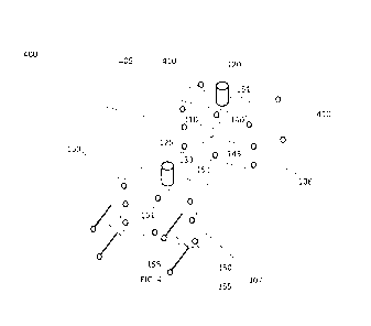
[0021] FIG. 1 illustrates an exemplary quantum electronic circuit device 100
in an assembled
state. FIG. 2 illustrates the exemplary quantum electronic circuit device 100
of FIG. 2 in an
unassembled state. The device includes housing 105 that includes a first
housing half 106
and a second housing half 107. As described herein, the first and second
halves 106, 107 are
a metallic material that has thermal and electrical conductivity sufficient
for cryogenic tem-
peratures such as but not limited to OFHC Cu and titanium (Ti). As described
herein, known
3D circuit QED devices are made from a superconducting material that provides
a good mag-
netic shield to external magnetic fields and suppresses the magnetic field
inside the cavity.
Superconducting resonators also allow high quality factors (Q) of
electromagnetic
eigenmodes of the cavity enclosure, while normal metal cavities are limited by
the finite sur-
face resistivity of metals at low temperatures. For a rectangular OFHC copper
cavity, this
limit is at about Q = 10,000, while superconducting aluminum cavities can
attain Q's of at a
least a few million. The quality factor of this mode is important as coupling
of the quantum
electronic circuit to it can produce a loss channel for the qubit if it is not
sufficiently high. In
exemplary embodiments, the limit of Q at approximately 10000 is sufficient for
long-live
quantum coherence, as described further herein. A cavity (resonator) is
defined within the
housing 105 when a first cavity half 110 and a second cavity half 115 are
brought together in
CA 02860516 2014-07-02
WO 2013/126120 PCT/US2012/068127
the assembled state. Assembled state means that the two cavity halves 110, 115
are brought
together to form a single resonant volume by securing in mechanical and
electrical contact a
first housing half 106 with a second housing half 107, with the chip 130
secured within the
cavity. The device 100 further includes one or more apertures in the cavity
enclosure that al-
low the application of an electromagnetic field to the cavity from an external
source. In pre-
sent embodiments these apertures are fitted with coaxial connectors 120, 125
coupled to the
housing 105 and configured to provide an electromagnetic field within the
cavity when con-
nected to an external electromagnetic field source. In this way the connectors
120, 125 act as
a electromagnetic field source to the device. External field sources can
include but are not
limited to microwave electronic equipment that generates a signal.
[0022] In exemplary embodiments, the device 100 further includes a qubit 130
disposed
within the housing 105 and within the cavity 110, 115 enclosed by the housing.
In the exam-
ples described herein, the qubit 130 contains a Josephson junction 135. FIG. 3
illustrates an
example of the qubit 130 as a superconducting transmon- style qubit. The qubit
130 includes a
sapphire substrate (other substrates are possible including Silicon) 131 and
two thin film
aluminum capacitor pads 132, 133 connected by a short wire 134 interrupted by
a single Jo-
sephson junction 135. The qubit 130 can be fabricated with a double-angle
evaporation pro-
cess using standard lithographic techniques. As described herein, it is
appreciated that other
types of superconducting qubits can be implemented including, but not limited
to, a phase
qubit, a fluxonium qubit, a capacitively shunted flux qubit, or any other
superconducting
qubit design which couples to the 3D cavity mode. Further it is appreciated
that yet other
types of qubits can be implemented that are based not on Josephson junctions
but on quantum
dots, nanowires, non-linear thin films, or electron or nuclear spins or
collections thereof,
among others.
[0023] The qubit 130 can be viewed as a dipole, with an associated dipole
moment vector.
The strength of its interaction with the cavity of the housing 105 is
determined predominantly
by the dot product of the dipole moment vector with the electric field vector
at the location of
the qubit 130. As such, adjustments of the qubit 130 location and orientation
relative to the
electric field profile of the mode of interest can be used to adjust the
strength of qubit-cavity
coupling. As such, the cavity can support multiple electromagnetic modes, with
strong cou-
6
CA 02860516 2014-07-02
WO 2013/126120 PCT/US2012/068127
pling between the cavity modes and the qubit 130. In exemplary embodiments,
the electro-
magnetic field sources connected via the connectors 120, 125 are configured to
induce a field
within the cavity that produces a measurement of an eigenstate of the qubit
130. In addition,
the electromagnetic field source is configured to induce transitions between
eigenstates. As
such, the qubit 130 has an associated transition frequency that enables the
qubit 130 to transi-
tion between eignstates when induced by the applied electromagnetic field.
[0024] In exemplary embodiments, the first housing half 106 further includes
recesses 140,
145 into which the qubit 130 is affixed. In this way, the qubit 130 is
recessed so it has clear-
ance when the device 100 is assembled. Furthermore the two cavity halves 110,
115 are
formed in such a manner that the depth and shape of each cavity as formed in
its respective
housing halves 106, 107 is predominantly identical to the other, producing in
the assembled
state a cavity that is bisected along a symmetry axis by the mechanical and
electrical contact
place of the housing halves 106, 107 and thus also the cavity halves 110, 115,
this symmetry
notwithstanding the requirement of the recesses 140, 145 to accommodate the
chip. In the
assembled state the qubit 130 is disposed in the resulting internal cavity as
described herein.
In exemplary embodiments, the qubit 130 is thus mechanically and thermally
coupled to the
housing 105 through the mechanical and thermal contact of the qubit chip or
substrate 131
with the housing at the location of the recesses 140, 145. The qubit 130 can
be further cou-
pled to the housing via any suitable coupling material that produces a
reliable thermal and
mechanical contract at the operating temperature. As described herein, the
entire device 100
can be cooled to the suitable cryogenic temperature. The thermal coupling as
described here-
in between the housing 105 and the qubit 130 allow the qubit to reach the
desired cryogenic
operating temperature.
[0025] As described herein, the housing 105 is machined from bulk OFHC copper.
The first
housing half 106 and the second housing half 107 divide the cavity (via the
first cavity half
110 and the second cavity half 115) with conducting walls along a symmetry
plane. The di-
viding plane is chosen so that the eignemode coupled to the qubit and used to
control and
measure the qubit 130 contains no surface currents crossing the dividing
plane. For the rele-
vant eigenmode, the surface currents flowing on the interior wall of the
cavity formed by the
7
CA 02860516 2014-07-02
WO 2013/126120 PCT/US2012/068127
cavity halves 110, 115 are perpendicular to the plane at which the housing
halves 106, 107
are brought into contact in the assembled state.
[0026] The OFHC copper cavity described in exemplary embodiments has a
measured quali-
ty factor of about 10,000 at 10mK, consistent with the known limit due to the
finite surface
conductivity of copper. As further described herein, the qubit 130 is disposed
in the recesses
140 145 on the first housing half 106, at the center of the enclosed volume in
the housing
105. The second housing half 107 is closed on top of the qubit 130. FIG. 4
illustrates an ex-
emplary quantum electronic circuit system 400. FIG. 4 illustrates that the
first housing half
106 and the second housing half 107 include holes 150 through which suitable
fasteners 155,
such as but not limited to, screws, mechanically secure the device 100 to a
metallic part 405
contiguous with the lowest temperature stage of a dilution refrigerator or
similar equipment
providing the cryogenic temperatures described herein. Additional holes 151
can be include
on the first housing half 106 and the second housing half 107 in order to
assemble the first
housing half 106 and the second housing half 107 prior to affixing the housing
105 to the me-
tallic part 405. The metallic part 405 includes holes 410 to receive the
fasteners 155. The
fastening of the first housing half 106 and the second housing half 107 create
a continuous
metal contact between the qubit 130 and the housing 105. When measured at
10mK, the de-
vice 100 has yielded a quantum coherence time T2* of up to 95 micro seconds.
[0027] In exemplary embodiments, a non-superconducting surface can be plated
in the inside
of the cavity halves 110, 115 as a thin (-1 micrometer) layer of
superconducting materials
such as Aluminum. In this way the cavity halves 110,115 are still thermally
well equilibrated
to the temperature of the dilution refrigerator because the housing halves
106, 107 remain
mostly OHFC copper, and the thin layer of superconducting material is thin
enough to not be
a large thermal impedance. With the plating of cavity halves 110,115, much
larger quality
factors then Q=10,000 are possible. It is appreciated that other methods
besides plating are
possible to produce a thin layer of superconducting material. It is also
appreciated that other
platings with non-superconducting materials such as gold may be sufficient to
also obtain
higher quality factors than Q-10,000
[0028] Several other observations can be made of the device 100, and system
400. First, the
electromagnetic modes occupy a region made up predominantly of free-space
(except for the
8
CA 02860516 2014-07-02
WO 2013/126120 PCT/US2012/068127
qubit substrate 131) defined by the cavity within the housing 105. The
physical properties of
the cavity including but not limited to the eigenmodes frequencies, quality
factors, and physi-
cal field conformations can be predicted and understood through analytical
treatment via
Maxwell's equations and/or through electromagnetic simulation. For example,
measurements
indicate that the modes are entirely controlled up to a maximum
characterization frequency of
27GHz. The presence of only understood and predictable modes that occupy a
free-space
region means the possible sources of loss within the system are far more
limited than in the
planar geometry. By placing the qubit 130 inside the cavity, the profile and
location of the
electromagnetic fields associated with the qubit mode can be adjusted in
addition to the elec-
tromagnetic field modes. It can be appreciated that appropriate modifications
have to be
made to the geometry of the qubit capacitance to obtain suitable capacitances
for both the
qubit eigenmode and the qubit-cavity coupling.
[0029] In exemplary embodiments, as described herein, the coupling of the
qubit 130 to the
cavity half 115 is implemented through the capacitance of the qubit circuit to
the cavity walls.
Measurements of the qubit 130 is performed by applying an electromagnetic
field to the cavi-
ty via the connectors 120, 125 and observing the reflected or transmitted
signal, whose ampli-
tude and phase are influenced by the eignestate of the qubit 130. In exemplary
embodiments
it is understood that the direct coupling of the qubit to the electromagnetic
field connectors is
non-existent or much weaker than the coupling via the fundamental mode of the
cavity. In
other words, there is no meaningful direct capacitance or inductance of the
qubit circuit to the
electromagnetic field connectors 120, 125. All interactions of the qubit with
the electromag-
netic environment external to the housing 105 are mediated by and filtered by
the eigenmodes
of the resonant cavity 110, 115 into which the qubit is affixed.
[0030] As described herein, the resonator provides a three-dimensional empty
volume with
conducting walls. The volume supports an electromagnetic eigenmode that
couples to the
qubit 130. The qubit 130 is contacted directly by normal metal parts which are
thermalized at
the desired operating temperature. The implementation of metal parts overcomes
the prob-
lems of thermal conductivity loss with using superconducting parts to form the
resonator. The
thermal conductivity of superconductors at temperatures below the transition
temperature can
9
CA 02860516 2014-07-02
WO 2013/126120 PCT/US2012/068127
be many orders of magnitude smaller than those of high-purity normal metals at
the same
temperature.
[0031] In exemplary embodiments, the device 100 can implement the normal metal
parts re-
quired for thermalization by constructing the housing 105 in entirety from
normal metal (ex-
cluding the qubit substrate 131and the qubit 130). In other exemplary
embodiments, the
qubit insulating substrate 131 can be mechanically contacted and thereby
thermally coupled
to just a smaller normal metal part that pierces the walls of an otherwise
superconducting 3D
cavity, and this normal metal part in turn thermally coupled to a reservoir at
the desired oper-
ating temperature Furthermore the housing 105 can be produced in entirety from
normal
metal, and subsequently coated on its interior wall a thin film of
superconducting material
excepting the chip seat at the recesses 140, 145 into which the chip is
affixed. In this manner
the cavity 110, 115 is bounded predominantly by a superconducting surface yet
the contact
points between the chip and the housing at the 140, 145 remain normal metal
and a contigu-
ous normal metal route is formed between the qubit chip 131 and the reservoir
at the desired
operating temperature. The implementation of metal directly on the qubit
substrate 131 solves
the problem of thermalization of the qubit and qubit substrate without the
necessity of remov-
ing certain properties of having a predominantly superconducting cavity. The
properties in-
clude the possibility to achieve much higher intrinsic cavity quality factors
(e.g., a measured
Q of an aluminum cavity of up to 4.4 million) and the shielding of the qubit
from externally-
produced magnetic field variations. Regardless of the implementation, the
normal metal
forms an uninterrupted path connecting the chip to a reservoir at a known and
desired operat-
ing temperature.
[0032] The terminology used herein is for the purpose of describing particular
embodiments
only and is not intended to be limiting of the invention. As used herein, the
singular forms
"a", "an" and "the" are intended to include the plural forms as well, unless
the context clearly
indicates otherwise. It will be further understood that the terms "comprises"
and/or "com-
prising," when used in this specification, specify the presence of stated
features, integers,
steps, operations, elements, and/or components, but do not preclude the
presence or addition
of one more other features, integers, steps, operations, element components,
and/or groups
thereof.
CA 02860516 2014-07-02
WO 2013/126120 PCT/US2012/068127
[0033] The corresponding structures, materials, acts, and equivalents of all
means or step
plus function elements in the claims below are intended to include any
structure, material, or
act for performing the function in combination with other claimed elements as
specifically
claimed. The description of the present invention has been presented for
purposes of illustra-
tion and description, but is not intended to be exhaustive or limited to the
invention in the
form disclosed. Many modifications and variations will be apparent to those of
ordinary skill
in the art without departing from the scope and spirit of the invention. The
embodiment was
chosen and described in order to best explain the principles of the invention
and the practical
application, and to enable others of ordinary skill in the art to understand
the invention for
various embodiments with various modifications as are suited to the particular
use contem-
plated
[0034] The flow diagrams depicted herein are just one example. There may be
many varia-
tions to this diagram or the steps (or operations) described therein without
departing from the
spirit of the invention. For instance, the steps may be performed in a
differing order or steps
may be added, deleted or modified. All of these variations are considered a
part of the
claimed invention.
[0035] While the preferred embodiment to the invention had been described, it
will be under-
stood that those skilled in the art, both now and in the future, may make
various improve-
ments and enhancements which fall within the scope of the claims which follow.
These
claims should be construed to maintain the proper protection for the invention
first described.
11