Note: Descriptions are shown in the official language in which they were submitted.
CA 02862177 2014-07-17
WO 2013/120096 PCT/US2013/025625
TRANSIENT CONTROL TECHNOLOGY CIRCUIT
CROSS REFERENCE TO RELATED APPLICATIONS
[0001] This application claims the benefit and priority of United States
Provisional Application
No. 61/597,631 entitled Transient Control Technology Circuit, filed on
February 10, 2012, the
entire contents of which are hereby incorporated by reference herein.
BACKGROUND
[00021 1. Field
[0003] The present disclosure relates generally to surge protection circuits
and improvements
thereof. More particularly, the present disclosure relates to automatically
resettable surge
protection circuits and improvements thereof.
[0004] 2. Description of the Related Art
[0005] Communications equipment, computers, home stereo amplifiers,
televisions and other
electronic devices are increasingly manufactured using a variety of electronic
components that
are vulnerable to damage from electrical energy surges. Surge variations in
power and
transmission line voltages, as well as noise, can change the operating
frequency range of
connected equipment and severely damage or destroy electronic devices.
Electronic devices
impacted by these surge conditions can be very expensive to repair or replace.
Therefore, a cost
effective way to protect these devices and components from power surges is
needed.
[0006] Surge protectors help protect electronic equipment from damage due to
the large
variations in the current and voltage resulting from lightning strikes,
svatching surges, transients,
noise, incorrect connections or other abnormal conditions or malfunctions that
travel across
power or transmission lines. Such protection schemes are particularly
important in the aerospace
industry where electronic reliability is often subject to heightened scrutiny
due to the increased
CA 02862177 2014-07-17
WO 2013/120096 PCT/US2013/025625
safety concerns inherent in airline industry operations. The effects of power
surges from
overvoltages or overcurrents upon commercial or military aircraft systems can
cause dangerous
disruptions of the various systems aboard the aircraft and must be mitigated
for safe airline
travel. As the number of electronic systems continues to increase on modern
aircraft, and
especially for flight critical electronics that impact air travel
characteristics or navigational
systems, it is important that such systems are not susceptible to damage or
malfunction due to a
power surge propagating through the system. In an effort to reduce these
risks, protection
circuits or devices have been incorporated as part of aircraft electrical
systems to prevent the
propagation of power surges through the electronics or other electrical
equipment.
[0007] However, conventional protection circuits typically employ fuses that
are configured to
open during an overcurrent fault condition. Other protection circuits use
passive surge protection
elements in a series or parallel configuration. Once these fuses or protection
elements have
opened or otherwise tripped to prevent propagation of a surge, the connected
electrical system
exists in a protected state, but the circuit can cause faults in a connected
system of the aircraft.
Indeed, due to the interoperability of many systems with each other for proper
aircraft
functionality or operation, the propagation of a fault from a first system to
a second system due
to a surge protection scheme may be extremely undesirable and damaging to safe
operation of
the aircraft.
[0008] Therefore, an active surge protection system or circuit is desirable
that can
automatically sense an overvoltage or overcurrent condition, actively respond
to the overvoltage
or overcurrent condition and automatically reset when the overvoltage or
overcurrent condition
returns to a normal state. The surge protection system should provide power
surge protection
such that a fault in one system does not propagate into or cause a fault in
another connected
2
CA 02862177 2014-07-17
WO 2013/120096 PCT/US2013/025625
system. In addition, the surge protection system or circuit would desirably be
inexpensive to
manufacture and lightweight while providing optimum coordination or behavior
of its surge
protection elements.
SUMMARY
[0009] An apparatus and method for automatically sensing a surge condition and
configured to
automatically reset when the surge condition has dissipated is disclosed. In
one implementation,
an automatic surge sensing protection device may include a housing defining a
cavity therein, an
input port connected to the housing and an output port connected to the
housing. A first
transistor may be positioned within the housing and have a first terminal, a
second terminal and a
third terminal, the first terminal connected to the input port and the second
terminal connected to
the output port. The first transistor may be configured to automatically
switch from a conducting
configuration to a non-conducting configuration, the conducting configuration
for allowing
signal propagation from the first terminal to the second terminal and the non-
conducting
configuration for preventing signal propagation from the first terminal to the
second terminal. At
least one resistor may be positioned within the housing and connected to the
third terminal of the
first transistor for biasing the first transistor. At least one diode may be
positioned within the
housing and connected to the input port for diverting a surge signal from the
input port to a
ground. A second transistor may be connected to the third terminal of the
first transistor for
controlling the switching of the first transistor from the conducting
configuration to the non-
conducting configuration.
BRIEF DESCRIPTION OF THE DRAWINGS
[0010] Other systems, methods, features, and advantages of the present
disclosure will be or
will become apparent to one of ordinary skill in the art upon examination of
the following figures
3
CA 02862177 2014-07-17
WO 2013/120096 PCT/US2013/025625
and detailed description. It is intended that all such additional systems,
methods, features, and
advantages be included within this description, be within the scope of the
present disclosure, and
be protected by the accompanying claims. Component parts shown in the drawings
are not
necessarily to scale, and may be exaggerated to better illustrate the
important features of the
present disclosure. In the drawings, like reference numerals designate like
parts throughout the
different views, wherein:
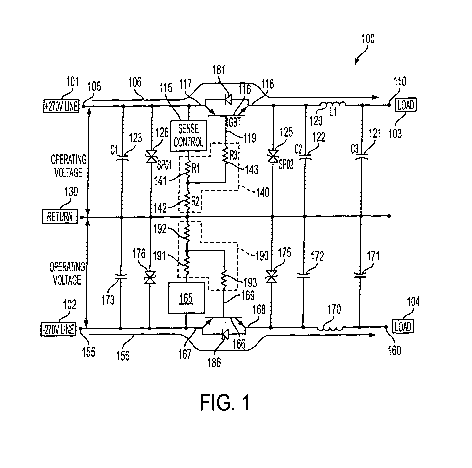
[00111 FIG. 1 is a schematic circuit diagram of a transient control technology
surge protection
circuit with dual power inputs and configured to automatically sense a surge
and reset after the
surge in accordance with an embodiment of the present invention;
[00121 FIG. 2 is a schematic circuit diagram of a transient control technology
surge protection
circuit with single power input and a positive polarity and configured to
automatically sense a
surge and reset after the surge in accordance with an embodiment of the
present invention; and
[00131 FIG. 3 is a schematic circuit diagram of a transient control technology
surge protection
circuit with single power input and a negative polarity and configured to
automatically sense a
surge and reset after the surge in accordance with an embodiment of the
present invention.
DETAILED DESCRIPTION
[0014] Referring to FIG. 1, a schematic circuit diagram of a transient control
technology surge
protection circuit 100 is shown. The surge protection circuit 100 operates to
protect any
connected loads (103, 104) from an electrical surge that could otherwise
damage or destroy the
loads (103, 104). The protected loads (103, 104) can be any form of electric
equipment, for
example electrical units aboard an aircraft, communications equipment, cell
towers, base
stations, PC computers, servers, network components or equipment, network
connectors or any
other type of surge sensitive electronic equipment. The surge protection
circuit 100 includes a
4
CA 02862177 2014-07-17
WO 2013/120096 PCT/US2013/025625
number of different electrical components, such as capacitors, resistors,
inductors, diodes and
IGBTs. For illustrative purposes, the surge protection circuit 100 will be
described with
reference to specific capacitor, resistor, inductor, diode or IGBT values and
configurations to
achieve specific surge protection or energy storage capabilities. However,
other specific
capacitor, resistor, inductor, diode or IGBT values or configurations may be
used to achieve
other electrical, surge protection or energy storage characteristics.
Similarly, although the
preferred configuration or implementation is shown with particular capacitor,
resistor, inductor,
diode and IGBT circuit elements and values, it is not required that the exact
circuit elements or
values described be used in the present disclosure. Thus, the capacitors,
resistors, inductors,
diodes and IGBTs are merely used to illustrate an implementation of the
present disclosure and
not to limit the present disclosure.
[0015] The surge protection circuit 100 may be implemented as a surge
protection or
suppression device. The surge protection circuit 100 includes a positive input
port 105 and a
positive output port 110 for connecting the surge protection device between a
positive voltage
source 101 and the load 103. Similarly, the surge protection circuit 100
includes a negative input
port 155 and a negative output port 160 for connecting the surge protection
device between a
negative voltage source 102 and the load 104. The voltage sources (101, 102)
may be 270 Vdc,
20A power sources. In one implementation, the surge protection circuit 100 may
be formed as
part of or included within a housing or other enclosure for allowing a user to
physically connect
the surge protection or suppression device to the voltage sources (101, 102)
and the loads (103,
104).
[0016] The input ports (105, 155) and output ports (110, 160) are configured
to mate or
otherwise interface with signal carrying conductors, for example, coaxial
cables. In some
CA 02862177 2014-07-17
WO 2013/120096 PCT/US2013/025625
implementations, the surge protection circuit 100 may be configured to operate
bi-directionally
such that a surge suppression device incorporating the circuit may have its
input ports function as
output ports or vice versa. By electrically connecting the surge suppression
device having the
surge protection circuit 100 along a conductive path or transmission line
between the power
sources (101, 102) and the connected loads (103, 104), an electrical surge
that could otherwise
damage or destroy the connected loads (103, 104) will instead be dissipated
through the surge
protection device. Conventional surge protection methods operate only to lower
the voltage
level presented to any connected equipment by diversion of surge current
through a surge
element (e.g., a silicon avalanche diode) along an alternate, parallel surge
path. A portion or
remnant of the surge is still presented at the connected equipment, however,
due to the let
through voltage or let through energy of the surge element. The surge
protection circuit 100
operates to block all of this surge voltage or current via incorporation of a
switching component
(e.g., an IGBT) in addition to surge current diversion, as described in
further detail herein. Thus,
the surge protection circuit 100 does not merely lower surge voltage levels
presented to systems
or equipment to be protected, but rather completely blocks all surge voltage
and diverts all surge
current from propagating to the connected systems or equipment, resulting in
zero surge energy
propagation to the connected systems or equipment.
[00171 The surge protection circuit 100 incorporates a signal path 106
extending from the
positive input port 105 to the positive output port 110. Similarly, a signal
path 156 extends from
the negative input port 155 to the negative output port 160. A ground or
return conductor 130 is
also included as part of the surge protection circuit 100. The return
conductor 130 may be a
signal line configured to be connected to an exterior ground via a connector
port or may be a part
of an exterior housing of the surge protection device. At each input port
(105, 155) each power
6
CA 02862177 2014-07-17
WO 2013/120096 PCT/US2013/025625
source (101, 102) is shown. At each output port (110, 160) each connected load
(103, 104) is
shown. In the absence of any further surge protection circuit elements, a
power surge from the
input ports (105, 155) would propagate along their respective signal paths
(106, 156) to the
output ports (110, 160) and potentially interfere with, cause damage to or
destroy the connected
loads (103, 104).
[0018] The surge protection circuit 100 includes various circuit elements
connected between
the input ports (105, 155), the output ports (110, 160) and the return
conductor 130 to prevent a
surge from interfering with the connected loads (103, 104). Not only are these
circuit elements
configured to automatically divert the surge before it reaches the connected
loads (103, 104), but
they are also configured to modify and automatically reset a signal path of
the surge protection
circuit 100 based upon operation of the surge protection circuit 100 under non-
surge or surge
conditions. Thus, a fault in the surge protection circuit 100 due to the
presence of a surge will
not propagate into or cause a fault in another connected system.
[0019] Turning more specifically to the various components used in the surge
protection
circuit 100, three capacitors (121, 122, 123) are provided, one end of each of
the capacitors (121,
122, 123) electrically connected with the return conductor 130 and the other
end connected to an
electrical node along the signal path 106 extending from the positive input
port 105 to the
positive output port 110. An inductor 120 is also connected along the signal
path 106. The three
capacitors (121, 122, 123) and the inductor 120 are elements of a pi filter to
account for any back
electromagnetic field (EMF) effects stemming from power supply sources,
inductive motor
loads, or other interfering devices connected at the input port 105 or the
load 103. Similarly,
three capacitors (171, 172, 173) are connected between the return conductor
130 and an electrical
node along the signal path 156 extending from the negative input port 155 to
the negative output
7
CA 02862177 2014-07-17
WO 2013/120096 PCT/US2013/025625
port 160. An inductor 170 is also connected along the signal path 156 to form
a pi filter with the
three capacitors (171, 172, 173) for similar reasons to those discussed above.
[0020] The surge protection circuit 100 also includes a first insulated gate
bipolar transistor
(IGBT) 116. The first IGBT 116 is a three terminal device with one terminal
117 (e.g., the
collector) connected to the positive input port 105 and a second terminal 118
(e.g., the emitter)
connected to the positive output port 110. When in a first, conducting
configuration, the IGBT
116 allows a signal present on the positive input port 105 to propagate to the
positive output port
110 along the signal path 106. A plurality of biasing resistors, or current
divider 140, including a
first resistor 141, a second resistor 142, and a third resistor 143, are
connected to a third terminal
119 (e.g., the gate) of the IGBT 116 for biasing the IGBT 116. The values of
the plurality of
resistors 140 are derived from the target operating voltage and load current
of the voltage sources
(101, 102). The first resistor 141, the second resistor 142 and the third
resistor 143 form a
current divider network to set the bias level and/or thresholds for operating
the IGBT 116 in a
second, non-conductive configuration when the current through the third
resistor 143 (i.e., the
gate current) is high enough to drive the IGBT 116 into its saturation region.
In one
implementation, the first resistor 141 may be about 65 ohms, the second
resistor 142 may be
about 2.7k ohms and the third resistor 143 may be about 1 ohm.
[0021] Similarly, a second IGBT 166 with three terminals is provided, one
terminal 167
connected to the negative input port 155 and a second terminal 168 connected
to the negative
output port 160. The same or similar to the description above for the first
IGBT 116, the second
IGBT 166 has a first, conducting configuration for allowing a signal present
on the negative
input port 155 to propagate along the signal path 156 to the negative output
port 160. A plurality
of biasing resistors, or current divider 190, including a fourth resistor 191,
a fifth resistor 192 and
8
CA 02862177 2014-07-17
WO 2013/120096 PCT/US2013/025625
a sixth resistor 193, are connected to a third terminal 169 of the second IGBT
166 for biasing the
IGBT 166, the same or similar to the discussion above for IGBT 116. The
resistors 190 may
have the same values as the respective resistors 140, as discussed above.
Flyback diodes (181,
186) may also be provided across the IGBTs (116, 166), respectively, for
providing additional
circuit protection when the voltage across the IGBTs (116, 166) is suddenly
reduced or removed.
100221 Zener diodes (126, 125) are connected between the return conductor 130
(i.e., ground)
and an electrical node along the signal path 106. Similarly, zener diodes
(176, 175) are
connected between the return conductor 130 and an electrical node along the
signal path 156.
When a surge signal is present along the signal path 106, the zener diodes
(126, 125) shunt at
least some of the surge energy to the return conductor 130 before it can
propagate to and
potentially damage the load 103. Likewise, when a surge signal is present
along the signal path
156, the zener diodes (176, 175) shunt at least some of the surge energy to
the return conductor
130 before it can propagate to and potentially damage the load 104. The zener
diodes (126, 125,
176, 175) may have any desired threshold voltage and may be selected based on
10% of the
maximum continuous operating voltage of the voltage sources (101, 102) or
selected based upon
a preferred or utilized surge diversion technology (e.g., Silicon Avalanche
Diodes (SADs), Metal
Oxide Varistors (MOVs), Gas Discharge Tubes (GDTs), etc.) for withstanding a
desired surge
amount for a given circuit.
100231 The combination of the zener diodes (126, 125, 176, 175) and the IGBTs
(116, 166)
provide reliable protection of equipment when subjected to power surge
waveforms. By utilizing
the zener diodes (126, 125, 176, 175) and the IGBTs (116, 166) together for
managing surge
energy, voltage let through that might otherwise introduce remnants of the
surge through to any
connected equipment if only the zener diodes (126, 125, 176, 175) were present
is instead
9
CA 02862177 2014-07-17
WO 2013/120096 PCT/US2013/025625
completely eliminated. Surge current flows entirely along a diverted surge
path through one or
more of the zener diodes (126, 125, 176, 175) because one or more of the IGBTs
(116, 166)
provides an open circuit for blocking the path of the surge to the connected
equipment. In this
manner, surge voltage or energy is not merely lowered, but nullified so far as
any connected
equipment is concerned. In one implementation, the power surge waveform to be
managed may
be a 2000V, 2000A 40/120 ps pulses per D0160 Waveform 5A requirements.
However, an
alternative implementation may be designed to accommodate any desired power
surge
waveform. In an alternative implementation, other circuit elements or
components may be
utilized for any of the zener diodes (126, 125, 176, 175) such as SADs, MOVs,
GDTs, etc.
Similarly, alternative switching components (e.g., relays, switches,
transistors, flip-flops,
contactors, etc.) may be utilized in place of or in addition to the IGBTs
(116, 166) in certain
implementations.
[0024J When a surge signal is introduced at the positive input port 105 and
diverted to the
return conductor 130, operation of the IGBT 116 changes from a first,
conducting configuration
to a second, non-conducting configuration. At least a portion of the surge
signal is permitted to
conduct through the sense control 115 and to the plurality of resistors 140.
The sense control
115 may be any circuit element or elements that does not conduct when
presented with a non-
surge signal, but begins to conduct when presented with a surge signal. When
in the second,
non-conducting configuration due to the biasing from the plurality of
resistors 140, the IGBT
116 prevents a signal present on the positive input port 105 from propagating
to the positive
output port 110 along the signal path 106.
[0025] Similar operation occurs when a surge signal present on the negative
input port 155 is
diverted to the return conductor 130. Operation of the second IGBT 166 changes
to a second,
CA 02862177 2014-07-17
WO 2013/120096 PCT/US2013/025625
non-conducting configuration due to biasing from the plurality of resistors
190 when at least a
portion of a surge signal is passed through a sense control 165. The second,
non-conducting
configuration of the second IGBT 166 prevents a signal at the negative input
port 155 from
propagating along the signal path 156 to the negative output port 160. The
IGBTs (116, 166)
may be capable of withstanding about 1,000V across their first terminals (117,
167) to second
terminals (118, 168) and capable of passing about 40A of current. When in the
first, conducting
configuration, the IGBTs (116, 166) exhibit a low continuous power loss (e.g.,
about 2.1 VCE).
[00261 In this manner, not only is a surge signal on the input ports (105,
155) automatically
sensed and directed or diverted away from the connected loads (103, 104), but
the signal paths
(106, 156) themselves leading from the input ports (105, 155) to the output
ports (110, 160) are
automatically opened via the IGBTs (116, 166) in response to the shunting of
the surge signal to
ground, thus preventing or mitigating the transmission of faults from part of
a system to another
in the event of a surge condition. After the surge signal is no longer present
on the input ports
(105, 155), the signal paths (106, 156) are automatically closed again via the
IGBTs (116, 166).
In an alternative implementation, any of a variety of signal pathways may be
automatically
changed as desired or designed in response to the sensing and/or diversion of
a surge signal to a
ground and then automatically reset after the surge signal is no longer
present.
[00271 Turning next to FIG. 2, a schematic circuit diagram of a transient
control technology
surge protection circuit 200 with single power input configured to
automatically sense a surge
and reset after the surge is shown, configured as a positive polarity circuit.
A power source 205
is connected to a load 250 through a variety of electronic components, as
discussed in greater
detail herein. In one implementation, the variety of electronic components may
be physically
mounted to a printed circuit board and configured to connect with the power
source 205 and/or
11
CA 02862177 2014-07-17
WO 2013/120096 PCT/US2013/025625
the load 250. In certain implementations, the electronic components may be
contained within a
housing or other enclosure with an input port for connecting with the power
source 205 and an
output port for connecting with the load 250. Certain structure or functional
aspects of the surge
protection circuit 200 may be or operate the same or similar to structure or
functional aspects of
the schematic circuit diagram 100, as previously described.
[0028] Turning more specifically to the variety of electronic components used
in the surge
protection circuit 200, a transistor 240 (e.g., an IGBT) with three connection
terminals (245, 246,
247) is provided for controlling a signal path, as discussed in more detail
herein. A power source
205 or other signal source is connected to the transistor 240 at a first
connection terminal 245 of
the transistor 240. A load 250 is connected to the transistor 240 at a second
connection terminal
246 of the transistor 240. Thus, a signal path 201 is formed from the power
source 205, through
the transistor 240 and to the connected load 250. During normal operation
(e.g., in the absence
of a surge condition), the transistor 240 is in a conducting configuration and
signals are allowed
to conduct through the transistor 240 along the signal path 201. However, upon
a surge
condition, the transistor 240 changes to a non-conducting configuration and
signals are prevented
from conducting through the transistor 240 along the signal path 201.
[0029] Resistors (220, 226) are connected to a third terminal 247 of the
transistor 240 and to
the power source 205 for helping bias the transistor 240 in the conductive
configuration or the
non-conductive configuration. Resistor 220 allows current to flow from the
power source 205
and into the resistor 226 when a surge condition is not present to bias the
transistor 240 into the
conducting configuration such that signals or power. may flow from the power
source 205 to the
load 250 along the signal path 201.
12
CA 02862177 2014-07-17
WO 2013/120096 PCT/US2013/025625
[0030] Zener diodes (210, 212, 214) are connected to the power source 205 for
diverting a
surge introduced into the signal path 201. Resistors (224, 222) are connected
to the zener diodes
(210, 212, 214). A second transistor 230 with three connection terminals (235,
236, 237) is also
provided for controlling the switching of the first transistor 240 from the
conducting
configuration to the non-conducting configuration or vice versa. The first
terminal 235 of the
second transistor 230 is connected to the third terminal 247 of the first
transistor 240 through the
resistor 226. The second terminal 236 of the second transistor 230 is
connected to a ground or a
return. The third terminal 237 of the second transistor 230 is connected to
the resistor 222.
Thus, when the surge encounters the zener diodes (210, 212, 214), the zener
diodes (210, 212,
214) sense the overvoltage condition and begin to conduct the surge current
into the resistor 224.
Current also flows into the resistor 222 and drives the second transistor 230
(e.g., an IGBT) so
that it begins to conduct between its first terminal 235 and its second
terminal 236.
[0031] When the second transistor 230 begins to conduct, current from the
resistor 220 flows
through the second transistor 230 instead of through the resistor 226. Thus,
the first transistor
240 is changed from its normal, conducting configuration to a non-conducting
configuration. A
flyback diode 242 is provided across the first transistor 240 for providing
additional protection
when the voltage across the first transistor 240 is suddenly reduced or
removed, similar to as
discussed above for FIG. 1. In an alternative implementation, a flyback diode
may also be
provided across the second transistor 230 in the same or similar manner.
[0032] Resistor 220 may be a 100k ohm resistor and resistor 224 may be a 47k
ohm resistor.
Resistors (226, 222) may be 1k ohm resistors. The first and second transistors
(240, 230) may
both be IRG4BC4OS IGBTs. The first transistor 240 may be selected to handle a
desired voltage
and/or current to provide optimum power transfer along the signal path 201
with low losses. An
13
CA 02862177 2014-07-17
WO 2013/120096 PCT/US2013/025625
IGBT may be used due to its fast switching capabilities and high power
handling capacity, but
may be more expensive and heavier than alternative switching components. The
second
transistor 230 may be chosen to be the same electrical component as the first
transistor 240 to
minimize the number of unique electrical parts within the circuit 200 or may
be selected to be
another transistor or switching device chosen to accommodate the signals
presented to it during
operation. The zener diodes (210, 212, 214) may be supplemented or replaced
with other surge
diverting elements (e.g., SADs, MOVs, GDTs, etc.). Different surge diverting
elements may
provide alternative surge diversion circuit performance (e.g., a GDT may
provide a longer delay
before the surge is diverted).
[0033] Turning next to FIG. 3, a schematic circuit diagram of a transient
control technology
surge protection circuit 300 with single power input configured to
automatically sense a surge
and reset after the surge is shown. The surge protection circuit 300 is a
negative polarity circuit
that operates similar to the surge protection circuit 200 shown in FIG. 2,
which is a positive
polarity circuit. A power source 305 is connected to a load 350 through a
variety of electronic
components, as discussed in greater detail herein. In one implementation, the
variety of
electronic components may be physically mounted to a printed circuit board and
configured to
connect with the power source 305 and/or the load 350. In certain
implementations, the
electronic components may be contained within a housing or other enclosure
with an input port
for connecting with the power source 305 and an output port for connecting
with the load 350.
Certain structure or functional aspects of the surge protection circuit 300
may be or operate the
same or similar to structure or functional aspects of the schematic circuit
diagram 100, as
previously described.
14
CA 02862177 2014-07-17
WO 2013/120096 PCT/US2013/025625
[0034] Turning more specifically to the variety of electronic components used
in the surge
protection circuit 300, a transistor 340 (e.g., an IGBT) with three connection
terminals (342, 343,
341) is provided for controlling a signal path, as discussed in more detail
herein. A power source
305 or other signal source is connected to the transistor 340 at a first
connection terminal 342 of
the transistor 340. A load 350 is connected to the transistor 340 at a second
connection terminal
343 of the transistor 340. During normal operation (e.g., in the absence of a
surge condition), the
transistor 340 is in a conducting configuration and signals are allowed to
conduct through the
transistor 340. However, upon a surge condition, the transistor 340 changes to
a non-conducting
configuration and signals are prevented from conducting through the transistor
340.
[0035] Resistors (326, 324) are connected to a third terminal 341 of the
transistor 340 and to a
ground 360 for helping bias the transistor 340 in the conductive configuration
or the non-
conductive configuration. Resistor 324 allows current to flow from the power
source 305 and
into the resistor 326 when surge conditions are not present to bias the
transistor 340 into the
conducting configuration such that signals or power may flow from the power
source 305 to the
load 350.
[0036] Zener diodes (310-317) are connected to the power source 305 for
diverting a surge.
Resistors (320, 322) are connected to the zener diodes (310-317). A second
transistor 330 with
three connection terminals (332, 333, 331) is also provided for controlling
the switching of the
first transistor 340 from the conducting configuration to the non-conducting
configuration or vice
versa. The second terminal 333 of the second transistor 330 is connected to
the third terminal
341 of the first transistor 340 through the resistor 326. The first terminal
332 of the second
transistor 330 is connected to the power source 305. The third terminal 331 of
the second
transistor 330 is connected to the resistor 322. Thus, when the surge
encounters the zener diodes
CA 02862177 2014-07-17
WO 2013/120096 PCT/US2013/025625
(310, 311), the zener diodes (310, 311) sense the overvoltage condition and
begin to conduct the
surge current into the resistor 320. Current also flows into the resistor 322
and drives the second
transistor 330 (e.g., an IGBT) so that it begins to conduct between its first
terminal 332 and its
second terminal 333.
[0037] When the second transistor 330 begins to conduct, current from the
resistor 324 flows
through the second transistor 330 instead of through the resistor 326. Thus,
the first transistor
340 is changed from its normal, conducting configuration to a non-conducting
configuration. A
flyback diode 345 is provided across the first transistor 340 for providing
additional protection
when the voltage across the first transistor 340 is suddenly reduced or
removed, similar to as
discussed above for FIG. 1. A flyback diode 335 is also provided across the
second transistor
330 in the same or similar manner.
[0038] Resistor 324 may be a 99k ohm resistor and resistor 320 may be a 48k
ohm resistor.
Resistors (326, 322) may be lk ohm resistors. The first and second transistors
(340, 330) may
both be IRG4BC4OS IGBTs. The first transistor 340 may be selected to handle a
desired voltage
and/or current to provide optimum power transfer with low losses. An IGBT may
be used due to
its fast switching capabilities and high power handling capacity, but may be
more expensive and
heavier than alternative switching components. The second transistor 330 may
be chosen to be
the same electrical component as the first transistor 340 to minimize the
number of unique
electrical parts within the circuit 300 or may be selected to be another
transistor or switching
device chosen to accommodate the signals presented to it during operation. The
zener diodes
(310-317) may be supplemented or replaced with other surge diverting elements
(e.g., SADs,
MOVs, GDTs, etc.). Different surge diverting elements may provide alternative
surge diversion
circuit performance (e.g., a GDT may provide a longer delay before the surge
is diverted).
16
CA 02862177 2014-07-17
WO 2013/120096 PCT/US2013/025625
[0039] The surge protection circuits 100, 200, or 300 described above may be
modified or
alternatively designed with differing circuit element values or with
different, additional, or fewer
circuit elements to achieve the same or similar functionality. The surge
protection circuits 100,
200, or 300 may also be scaled for application of any desired voltage or
current operating levels.
The surge protection circuits 100, 200, or 300 may be designed with components
to facilitate AC
functionality or DC functionality. As such, the surge protection circuits 100,
200, or 300 may be
configured for ranges of typical or commonly expected surge levels or may be
designed and
constructed as a custom configuration to meet a particular system or setup. By
utilizing a small
number of electrical components to achieve the desired functionality,
manufacturing cost may be
reduced and the weight of an apparatus incorporating the circuit kept low.
[0040] The circuit elements incorporating the surge protection circuits 100,
200, or 300 may be
discrete elements positioned within an enclosure or housing and/or may be
mounted or
electrically connected with a printed circuit board. An enclosure used may
have input and/or
output ports for allowing user-installation of the circuit to their own
systems or equipment. In
certain implementations, the enclosure may be a connector, the various circuit
elements
integrated within the connector.
[0041] Exemplary implementations of the present disclosure have been disclosed
in an
illustrative style. Accordingly, the terminology employed throughout should be
read in a non-
limiting manner. Although minor modifications to the teachings herein will
occur to those well
versed in the art, it shall be understood that what is intended to be
circumscribed within the scope
of the patent warranted hereon are all such implementations that reasonably
fall within the scope
of the advancement to the art hereby contributed, and that that scope shall
not be restricted,
except in light of the appended claims and their equivalents.
17