Note: Descriptions are shown in the official language in which they were submitted.
ELECTROLUMINESCENT DEVICES AND THEIR MANUFACTURE
This application claims priority to U.S. patent application no. 13/677,864,
filed
November 15, 2012, which is a continuation of U.S. patent application no.
13/624,910,
filed September 22, 2012, which claims priority to U.S. provisional patent
application no.
61/582,581, filed January 3, 2012.
Field
The present invention relates to a system for producing electroluminescent
devices
having a lower backplane electrode layer and an upper electrode layer, the
lower and upper
tO electrode layers being connectable to an electrical driving circuit. One
or more functional
layers are disposed between the lower and upper electrode layers to form at
least one
electroluminescent area.
Backuound
Since the 1980s, electroluminescent (EL) technology has come into widespread
use
in display devices where its relatively low power consumption, relative
brightness and
ability to be formed in relatively thin-film configurations have shown it to
be preferable to
light emitting diodes (LEDs) and incandescent technologies for many
applications.
Commercially manufactured EL devices have traditionally been produced using
doctor blade coating and printing processes such as screen printing or, more
recently, ink
jet printing. For applications that require relatively planar EL devices these
processes have
worked reasonably well, as they lend themselves to high-volume production with
relatively
efficient and reliable quality control.
However, traditional processes are inherently self limiting for applications
where it
is desirable to apply an EL device to a surface having complex topologies,
such as convex,
concave and reflexed surfaces. Partial solutions have been developed wherein a
relatively
thin-film EL "decal" is applied to a surface, the decal being subsequently
encapsulated
within a polymer matrix. While moderately successful, this type of solution
has several
inherent weaknesses. Firstly, while decals can acceptably conform to mild
concave/con-vex topologies, they are incapable of conforming to tight-radius
curves
without stretching or wrinkling. In addition, the decal itself does not form
either a
chemical or mechanical bond with an encapsulating polymer, essentially
remaining a
foreign object embedded within the encapsulating matrix. These weaknesses pose
difficulties in both manufacturing and product life-cycle, as embedded-decal
EL lamps
CA 2862546 2019-05-09
CA 02862546 2014-06-30
WO 2013/102859 PCT/IB2013/050037
2
applied to complex topologies are difficult to produce and are susceptible to
delamination
due to mechanical stresses, thermal stresses and long-term exposure to
ultraviolet (UV)
light. There remains a need for a way to produce an EL lamp that is compatible
with items
having a surface incorporating complex topologies.
Summary
A process is disclosed according to an embodiment to the present invention
whereby an EL device is `Tainted" onto a surface or "substrate" of a target
item to which
the EL device is to be applied. The present invention is applied to the
substrate in a series
of layers, each of which performs a specific function integral to the process.
One object of the present invention is a process for producing a conformal
electroluminescent system. The process includes the step of selecting a
substrate. A base
backplane film layer is applied upon the select substrate using an aqueous-
based,
electrically conductive backplane material. A dielectric film layer is applied
upon the
backplane film layer using an aqueous-based dielectric material. A phosphor
film layer is
applied upon the dielectric film layer using an aqueous-based phosphor
material, the
phosphor film layer being excited by an ultraviolet radiation source during
application.
The ultraviolet radiation source provides visual cues while the phosphor film
layer is being
applied, and the application of the phosphor film layer is adjusted in
response to the visual
cues to apply a generally uniform distribution of the phosphor material upon
the dielectric
film layer. An electrode film layer is applied upon the phosphor film layer
using an
aqueous-based, substantially transparent, electrically conductive electrode
material. The
backplane film layer, dielectric film layer, phosphor film layer, and
electrode film layer are
each preferably applied by spray conformal coating. The phosphor film layer is
excitable
by an electrical field established across the phosphor film layer upon
application of an
electrical charge between the backplane film layer and the electrode film
layer such that
the phosphor film layer emits electroluminescent light.
Brief Description of the Drawings
Further features of the inventive embodiments will become apparent to those
skilled in the art to which the embodiments relate from reading the
specification and
claims with reference to the accompanying drawings, in which:
Fig. 1 is a schematic layer diagram of an EL lamp according to an embodiment
of
the present invention;
CA 02862546 2014-06-30
WO 2013/102859 PCT/IB2013/050037
3
Fig. 2 is a flow diagram of a process for producing electroluminescent lamps
according to an embodiment of the present invention;
Fig. 3 is a schematic layer diagram of an EL lamp showing routing of
conductive
elements according to an embodiment of the present invention;
Fig. 4 is a schematic layer diagram of an EL lamp showing routing of
conductive
elements according to another embodiment of the present invention;
Fig. 5 is a flow diagram of a process for applying a phosphor layer according
to an
embodiment of the present invention;
Fig. 6 is a schematic layer diagram of an EL lamp having a tinted overcoat
according to an embodiment of the present invention;
Fig. 7 is a schematic layer diagram showing light being reflected from the
tinted
overcoat of Fig. 6 and giving color effect to the light;
Fig. 8 is a schematic layer diagram showing light passing through the tinted
overcoat of Fig. 6, providing an augmenting color effect to reflected light;
Fig. 9 is a schematic layer diagram of a multiple-layer EL lamp with top-layer
wiring according to an embodiment of the present invention;
Fig. 10 is a schematic layer diagram of a multiple-layer EL lamp with bottom-
layer
wiring according to another embodiment of the present invention;
Fig. 11 is a schematic layer diagram of a multiple-layer EL lamp with dual-
layer
wiring according to yet another embodiment of the present invention;
Fig. 12 is a schematic layer diagram of a multiple-layer EL lamp with dual-
layer
wiring according to still another embodiment of the present invention; and
Fig. 13 is a schematic layer diagram of an EL lamp having a transparent
substrate
according to yet another embodiment of the present invention.
Detailed Description
In the discussion that follows, like reference numerals are used to refer to
like
elements and structures in the various figures.
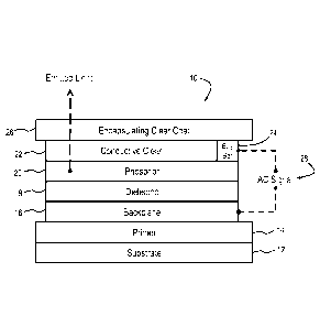
The general arrangement of a conformal EL lamp 10 is shown in Fig. 1 according
to an embodiment of the present invention. EL lamp 10 comprises a substrate
12, a primer
layer 14, an electrically conductive backplane electrode layer 16, a
dielectric layer 18, a
phosphor layer 20, a substantially transparent, electrically conductive top
electrode 22, a
bus bar 24 and an optional encapsulating layer 26.
CA 02862546 2014-06-30
WO 2013/102859 PCT/IB2013/050037
4
Substrate 12 may be a select surface of any suitable target item upon which EL
lamp 10 is to be applied. Substrate 12 may be conductive or non-conductive,
and may
have any desired combination of convex, concave and reflexed surfaces. In some
embodiments of the present invention substrate 12 is a transparent material
such as,
without limitation, glass or plastic.
Primer layer 14 is a non-conductive film coating applied to substrate 12.
Primer
layer 14 serves to electrically insulate substrate 12 from subsequent
conductive and semi-
conductive layers, discussed further below. Primer layer 14 also preferably
promotes
adhesion between substrate 12 and subsequent layers.
Conductive backplane 16 is a film coating layer that is preferably masked over
primer layer 14 to form a bottom electrode of EL lamp 10. Conductive backplane
16 is
preferably a sprayable conductive material and may form the rough outline of
the lit EL
"field" of the finished EL lamp 10. The material selected for backplane 16 may
be tailored
as desired to suit various environmental and application requirements. In one
embodiment
backplane 16 is made using a highly conductive, generally opaque material.
Examples of
such materials include, without limitation, an alcohol/latex-based, silver-
laden solution
such as SILVASPRAYTm available from Caswell, Inc. of Lyons New York, and a
water-
based latex, copper-laden solution such as "Caswell Copper" copper conductive
paint, also
available from Caswell, Inc.
In one embodiment a predetermined amount of silver flake may be mixed with the
copper conductive paint. Empirical testing has shown that the addition of
silver flake
significantly enhances the performance of the copper conductive paint without
adversely
affecting its relatively environmentally-friendly characteristics.
As an alternative to either Caswell SILVASPRAYTM or Caswell Copper, silver
flake may be mixed in a solution of an aqueous-based styrene acrylic co-
polymer solution
(discussed further below) and ammonia to encapsulate the silver for
application to a
prepared surface (i.e., substrate) as a backplane 16 material.
Conductive backplane 16 may also be a metal plating wherein a suitable
conductive metal material is applied to a non-conductive substrate 12 using
any suitable
process for the select metal plating. Example types of metal plating include,
without
limitation, electroless plating, vacuum metalizing, vapor deposition and
sputtering.
Preferably, the resulting electrically conductive backplane 16 has a
relatively low
resistance to minimize voltage gradients across the surface of the backplane
to allow for
CA 02862546 2014-06-30
WO 2013/102859 PCT/IB2013/050037
the proper operation of the electroluminescent system (i.e., sufficient lamp
brightness and
brightness uniformity). In some embodiments the resistance of a plated
backplane 16 is
preferably less than about one ohm per square inch of surface area.
Conductive backplane 16 may also be an electrically conductive, generally
clear
5 layer such as, without limitation, "CLEVIOSTm S V3" and or "CLEVIOSTM S
V4"
conductive polymers, available from Heraeus Clevios GmbH of Leverkusen,
Germany.
This configuration may be preferred for use with target items having generally
transparent
substrates, such as glass and plastic, and for embodiments where a thinner
total application
of layers for EL lamp 10 is desired.
Dielectric layer 18 is an electrically non-conductive film coating layer
comprising a
material (typically Barium Titanate - BaTiO3) possessing high dielectric
constant
properties encapsulated within an insulating polymer matrix having relatively
high
permittivity characteristics (i.e., an index of a given material's ability to
transmit an
electromagnetic field). In one embodiment of the present invention dielectric
layer 18
comprises about a 2:1 solution of co-polymer and dilute ammonium hydroxide. To
this
solution a quantity of BaTiO3, which has been pre-wetted in ammonium
hydroxide, is
added to form a supersaturated suspension. In various embodiments of the
present
invention dielectric layer 18 may comprise at least one of a titanate, an
oxide, a niobate, an
aluminate, a tantalate, and a zirconate material, among others.
Dielectric layer 18 serves two functions. Firstly, dielectric layer 18
provides an
insulating barrier between backplane layer 16 and the superimposed semi-
conductive
phosphor 20, top electrode 22 and bus bar 24 layers. In addition, because of
the unique
electromagnetic polarization characteristics of the dielectric materials,
dielectric layer 18
serves to enhance the performance of the electromagnetic field generated
between the
backplane 16 and top electrode 22 layers when an AC signal 28 is applied
between the
backplane and the top electrode, the AC signal generating an electrical field
or electrical
charge between the backplane and the top electrode. In addition, despite being
an efficient
electrical insulator, the high dielectric quality of the BaTiO3 and the high
permittivity of
the polymer matrix are highly permeable to the electrostatic field generated
between
backplane 16 and top electrode 22
Furthermore, in multiple-layer EL lamp applications a dielectric layer 18
having
photorefractive qualities may be selected wherein an index of refraction of
the dielectric
layer is affected by an electric field applied to backplane 16 and electrode
22 by AC signal
CA 02862546 2014-06-30
WO 2013/102859
PCT/IB2013/050037
6
28 (Fig. 1). These photorefractive qualities of the select dielectric layer 18
material may
be utilized to facilitate the propagation of light through superimposed layers
of the EL
lamp. A non-limiting example material having photorefractive properties is
BaTiO3.
Phosphor layer 20 is a semi-conductive film coating layer comprised of a
material
(typically metal-doped Zinc Sulfide (ZnS)) encapsulated within a highly
electrostatically
permeable polymer matrix. When excited by the presence of an alternating
electrostatic
field generated by AC signal 28, the doped ZnS absorbs energy from the field,
which it in
turn re-emits as a visible-light photon upon returning to its ground state.
Phosphor layer
20 serves two functions. Firstly, while the metal-doped Zinc Sulfide phosphor
is
technically classed as a semiconductor, when encapsulated within the co-
polymer matrix,
it further effectively provides an additional insulating barrier between the
backplanc 16
layer and the superimposed top electrode 22 and bus bar 24 layers. In
addition, once
excited by the presence of an alternating electromagnetic field, phosphor
layer 20 emits
visible light.
In one embodiment of the present invention phosphor layer 20 comprises about a
2:1 solution of co-polymer and dilute ammonium hydroxide. To this solution, a
quantity
of metal-doped Zinc Sulfide based phosphors doped with at least one of copper,
manganese and silver (i.e., ZnS :Cu, Mn, Ag, etc.) pre-wetted in a dilute
ammonium
hydroxide is added to form a supersaturated suspension.
Preferably, an aqueous-based styrene acrylic co-polymer solution (hereafter
"co-
polymer") is utilized as an encapsulating matrix for both dielectric layer 18
and phosphor
layer 20. This material is suitable for close-proximity and long-term contact
without
adverse impact to organisms or the environment. An example co-polymer is
DURAPLUSTM polymer matrix, available from the Dow Chemical Company of Midland,
Michigan. A significant advantage of the co-polymer is that it provides a
chemically
benign and versatile bonding mechanism for a variety of sub- and top-coating
options on a
select substrate 12. Ammonium hydroxide may be used as a thinner/drying agent
for the
co-polymer.
During production of EL lamp 10, after volatile components of the co-polymer
solution of dielectric layer 18 and phosphor layer 20 have been eliminated
(typically by
evaporation) during a curing process, the resultant coatings are largely
chemically inert.
As such, the dielectric layer 18 and phosphor layer 20 coatings do not readily
react
CA 02862546 2014-06-30
WO 2013/102859 PCT/IB2013/050037
7
chemically with under- or over-lying layers and, as a result, encapsulates and
protects the
homogeneous dielectric 18 and phosphor particle 20 layer distributions.
Chemically, during a curing process, open ends of a long-chain co-polymer of
dielectric layer 18 and phosphor layer 20 are exposed. This provides a ready
mechanism
for the creation of a strong mechanical bond between chemically dissimilar
layers, as the
exposed polymer chain ends essentially act as a "hook" analogous to the hook
portion of a
hook-and-loop fastener. These hooks provide a relatively porous surface
topology that
readily accepts infiltration by the application of a second long-chain polymer
solution. As
the secondary layer cures, its polymer chain ends are exposed and essentially
"knit" with
the aforementioned exposed co-polymer ends to form a strong mechanical bond
between
adjacent layers.
Top electrode 22 is a film coating layer that is preferably both electrically
conductive and generally transparent to light. Top electrode 22 may be from
such
materials as, without limitation, conductive polymers (PEDOT), carbon
nanotubes (CNT),
antimony tin oxide (ATO) and indium tin oxide (ITO). A preferred commercial
product is
CLEVIOSIm conductive, transparent and flexible polymers (available from
Heraeus
Clevios GmbH of Leverkusen, Germany) diluted in isopropyl alcohol as a
thinner/drying
agent. CLEVIOS TM conductive polymers exhibit relatively high efficacy and are
relatively
environmentally benign. In addition, CLEVIOS TM conductive polymers are based
on a
styrene co-polymer and thus provides a ready mechanism for chemical
crosslinking/mechanical bonding with the underlying phosphor layer 20.
Alternate materials may be selected for top electrode 22 solutions, including
those
containing Indium Tin Oxide (ITO) and Antimony Tin Oxide (ATO). However, these
are
less desirable than CLEVIOSTM conductive polymers due to greater environmental
concerns.
In some embodiments of the present invention it may be desirable for backplane
electrode layer 16 to be generally transparent. In such cases any of the
materials discussed
above for top electrode 22 may be utilized for backplane electrode layer 16.
The efficiency of top electrode 22 materials are hampered by their divergent
operating requirements; that of both being electrically conductive while also
being
generally transparent to visible light. As the area of lit fields of an EL
lamp 10 become
larger, a point of diminishing returns is approached wherein the thickness of
the top
electrode layer 22 to achieve a sufficiently low resistivity for the necessary
voltage
CA 02862546 2014-06-30
WO 2013/102859 PCT/IB2013/050037
8
distribution across the top electrode layer becomes optically inhibitive or,
conversely, the
thickness of the top electrode becomes unacceptably electrically inefficient.
As a result, it
is often desirable to augment the transparent top electrode layer 22 with a
more efficient
electrical conductor as close to the lit field at possible, in order to
minimize the thickness
of top electrode layer for optimum optical characteristics. Bus bar 24
fulfills this
requirement by providing a relatively low-impedance strip of conductive
material, usually
comprised of one or more of the materials usable to produce as conductive
backplane 16.
Bus bar 24 is typically applied to the peripheral edge of the lit field.
Although bus bar 24 is generally shown as adjacent to top electrode layer 22
in the
figures, in practice the bus bar may be applied upon (i.e., atop) the top
electrode layer.
Conversely, top electrode layer 22 may be applied upon (i.e., atop) the bus
bar 24.
Once applied, top electrode 22 and bus bar 24 are susceptible to damage due to
scratches or marking. After curing the top electrode 22 and bus bar 24 it is
preferable to
encapsulate EL lamp 10 with an encapsulating clear coat film layer 26 such as
a clear
polymer 26 of suitable hardness to protect the EL lamp from damage.
Encapsulating layer
26 is preferably an electrically insulating material applied over the EL lamp
10 stack-up,
thereby protecting the lamp from external damage. Encapsulating layer 26 is
also
preferably generally transparent to light emitted by the EL lamp 10 stack-up
and is
preferably chemically compatible with any envisioned topcoating materials for
the target
item of substrate 12 that provide a mechanism for chemical and/or mechanical
bonding
with topcoating layers. Encapsulating layer 26 may be comprised of any number
of
aqueous, enamel or lacquer-based products.
As previously noted, current EL products are limited to application to
relatively
simple topographical surfaces that are planar or nearly planar. This is
because
.. screen/inkjet print-based processes require a flat or nearly flat surface
to assure proper
distribution ratios of the required components in the respective layers.
Unlike print-based
EL production processes, primer layer 14, backplane 16, dielectric layer 18,
phosphor layer
20, conductive top electrode 22, bus bar 24 and encapsulating layer 26 are
preferably
formulated to be compatible with and applied by both tools and methods
commonly
available to and within the purview of the painter's craft. Thus, EL lamp 10
may be
"painted" onto substrate 12 as a stackup of conformal coats comprising primer
layer 14,
backplane 16, dielectric layer 18, phosphor layer 20, conductive top electrode
22, bus bar
24 and encapsulating layer 26. By utilizing select components of the
respective layers and
CA 02862546 2014-06-30
WO 2013/102859 PCT/IB2013/050037
9
application techniques as disclosed herein that are compatible with spray-
based equipment,
EL lamps 10 may be applied to a wide variety of materials and/or complex
topologies such
that any "paintable" substrate 12 surface can be utilized for the application
of a conformal,
energy-efficient EL lamp. Accordingly, EL lamp 10 is "conformal" in the sense
that it
conforms to the shape and geometry of substrate 12.
With reference to Fig. 2 in combination with Fig. 1, a process s100 for
producing
EL lamps will now be described.
At s102 a substrate 12 is selected. Substrate 12 is typically a surface of a
select
target item, which may be made from any suitable conductive or non-conductive
material,
and may have any desired contours and shapes.
A primer layer 14 is applied to substrate 14 at s104. Whether the intended
target
item substrate 12 is conductive, i.e., metal, or carbon fiber or non
conductive, i.e., some
form of glass, plastic, fiberglass or composite material, it is preferable to
apply a quantity
of a compatible oxide-based primer to the substrate in a relatively thin layer
to seal the
is surface, provide electrical insulation between the substrate and the EL
lamp 10, and insure
adhesion with overlying topcoat layers. In some circumstances, it may also be
desirable to
apply at s106 a thin layer of a suitable enamel/lacquer/aqueous paint,
compatible with the
intended topcoat, over the oxide primer layer. "Topcoat" as used herein refers
generally to
any coating placed over the finished EL lamp 10, such as a translucent coating
covering
the EL lamp and portions of substrate 12 not covered by the EL lamp. The
optional
painting step of s106 is particularly attractive when the target item
comprising substrate 12
is to be subjected to prolonged handling before further EL lamp 10 layers are
applied.
Because of the relative "softness" of oxide-based primers, exposed primer
surfaces can be
degraded by frequent handling and the resultant oxide dust can stain the raw
surface.
For each EL "lit field" on a given surface, two electrical connections are
provided
at s108 to provide a pathway for the AC signal 28 (Fig. 1) that excites
phosphor layer 20.
There are two basic mechanisms for installing these electrical pathways, the
selection of
which is determined by the characteristics of the substrate 12 of the target
item. With
additional reference to Fig. 3, for non-conductive plastic, fiberglass or
composite target
item substrates 12, it is preferable to provide one or more "carrythrough"
conductive
elements 30-1, 30-2 to backplane 16 and bus bar 24 respectively of EL lamp 10
via small
openings 32 in substrate 12 of the target item and primer layer 14 to provide
electrical
contact with the overlying backplane and bus bar.
CA 02862546 2014-06-30
WO 2013/102859 PCT/IB2013/050037
For some forms of conductive substrate 12 target items, the carrythrough
technique
is also effective, given the inclusion of an insulating sheath 34 between the
substrate and
the signal pathway. This is both a practical and a safety consideration, as
the electrical
current demand placed on the system by needlessly energizing the
substrate/target item
5 significantly reduces the power consumption efficiency of the system as a
whole and
increases safety by electrically isolating the EL lamp 10 field from a
conductive substrate
12 of the target item and any pathways to a ground state, such as a defect in
the substrate
of the target item.
When structural or practical considerations (such as maintaining the integrity
of a
10 fluid containment vessel) prohibit using the aforementioned carrythrough
technique of Fig.
3 on a substrate 12 of a target item, signal paths to EL lamp 10 may be
provided by
embedding conductive elements 30-1 and 30-2 within the insulating primer layer
14 and, if
required, "wrap around" a panel edge as shown in Fig. 4. Either of the method
of Figs. 3
and 4 for providing signal access to the backplane 16 and bus bar 24, i.e.,
"carrythrough"
or "wrap around," are functionally equivalent and may be selected based upon
particular
conditions and requirements imposed by the substrate 12 of the target item.
Backplane layer 16 is applied at s110. Backplane layer 16, as previously
discussed,
is a pattern comprising a conductive material and is masked over the primer 14
coating.
Backplane layer 16 may be applied to any suitable thickness, such as about
0.001 inches,
preferably using an airbrush or sufficiently fine-aperture gravity-feed type
spray
equipment. When so applied, backplane layer 16 is placed into electrical
contact with
conductive element 30-1 (Figs. 3, 4) to provide electrical contact with AC
signal 28 and
also defines the rough outline of the lit EL lamp 10 field.
Dielectric film layer 18 is spray-applied at step s112. The previously-
described
.. supersaturated dielectric solution is applied using suction and/or pressure
feed type spray
equipment under visible light at a predetermined air pressure, adjusted for
variables such
as ambient temperature and topology of the substrate 12 target item.
Dielectric layer 18 is
preferably applied at ambient air temperatures of about 70 degrees Fahrenheit
or greater.
The dielectric layer is preferably applied in successive thin coats of
solution to ensure even
distribution of the BaTiO1 particulate/polymer solution and prevent excessive
buildup that
could overcome the surface tension of the solution, which in turn can create a
"run" or
"droop" within the applied layers. Excessive buildup of material that results
in running or
drooping of the applied layers leads to an uneven congregation of the
encapsulated
CA 02862546 2014-06-30
WO 2013/102859 PCT/IB2013/050037
11
particulate (referred to as "sand duning") that has a detrimental direct
effect on the
appearance of the final product. Therefore, it is often desirable to augment
the initial air
curing of successive applied layers by the application of enhanced infra-red
radiation from
sources such as direct sunlight and enhanced-infrared lamps between coats for
a
.. determinable period of time, depending upon ambient temperature and
humidity
conditions.
Phosphor layer 20 is applied at s114. The previously-discussed supersaturated
phosphor solution is applied using suction and/or pressure feed type spray
equipment at a
predetermined air pressure, adjusted for variables such as ambient temperature
and
.. topology of the substrate 12 of the target item. The phosphor layer 20 is
preferably applied
proximate (e.g., under) an ultraviolet radiation source such as a long-wave
ultraviolet light
(e.g., UV "A" or "black light" ultraviolet light) to enhance visible
indicators or cues to the
operator during application, to ensure relatively uniform particulate
distribution. The
phosphor layer 20 is preferably applied at ambient air temperatures of about
70 degrees
Fahrenheit or greater. The phosphor layer 20 is preferably applied in
successive thin coats
of solution to ensure even distribution of the ZnS-particulate/polymer
solution, and to
prevent excessive buildup could overcome the surface tension of the solution,
in turn
creating a "run" or "droop" within the applied phosphor layers. Like
dielectric layer 18,
excessive buildup of material that results in "running" or drooping" of the
applied layers
may lead to an uneven congregation of the encapsulated particulate (i.e.,
"sand duning")
that has a detrimental direct effect on the appearance of the final product.
Therefore, it is
preferable to augment the initial air curing of successive applied layers by
the application
of enhanced infra-red radiation by such sources as direct sunlight and
enhanced-infrared
lamps between coats for a determinable period of time, depending on ambient
conditions
such as temperature and humidity.
Further details of the application of phosphor layer 20 are shown in Fig. 5.
The
previously-discussed supersaturated phosphor solution is applied using suction
and/or
pressure feed type spray equipment at a predetermined air pressure, adjusted
for variables
such as ambient temperature and topology of the substrate 12 of the target
item. Phosphor
layer 20 is preferably applied under the aforementioned ultraviolet radiation
source to
enhance visible indicators or cues to the operator during application, to
ensure relatively
uniform particulate distribution.
CA 02862546 2014-06-30
WO 2013/102859 PCT/IB2013/050037
12
At s114-1, prior to the application of phosphor layer 20 an operator
preferably
arranges an ultraviolet radiation source in such a manner that the ultraviolet
radiation
source will generally evenly illuminate a target item to be painted. The
ultraviolet
radiation source is preferably located in a room or other area that is
darkened or otherwise
substantially devoid of other light sources, so that the ultraviolet radiation
source is the
primary source of illumination upon the object being painted.
Phosphor layer 20 is applied to the substrate 12 of the target item at s114-2.
When
applying the phosphor layer, the operator observes that it will glow brightly
under the
ultraviolet radiation source. This provides a visual cue for the quality of
the coating,
whereas under a typical ambient white light the operator is not be able to
distinguish the
phosphor layer 20 from dielectric layer 18 because the two layers will blend
visually.
At s114-3, as the operator preferably applies a phosphor film layer 20
comprising
one or more relatively thin coats of phosphor under the ultraviolet radiation
source the
operator will note that the phosphor layer coating becomes more uniform and,
accordingly,
will know where to apply more or less phosphor layer coating in order to
ensure the
finished phosphor layer is as uniform as desired. The phosphor film layer 20
being applied
is excited by the aforementioned ultraviolet radiation source during
application, the
ultraviolet radiation source thereby providing the operator with visual cues
while the
phosphor film layer is being applied. At s114-4 the operator adjusts the
application of the
phosphor film layer 20 in response to the visual cues to apply a generally
uniform
distribution of the phosphor material upon the dielectric film layer 18. In
some
embodiments a phosphor layer of about 0.001 inches or less is preferred. The
conformal
coating process is finished at s114-5 once the phosphor film layer 20 has
reached the
desired thickness and uniformity.
Since the dielectric 18 and phosphor 20 layer components of the present
invention
are chemically identical aside from inert particulate components, functionally
they are
applied in a contiguous process that chemically forms a single heterogeneous,
chemically
crosslinked layer distinguished only by the encapsulated inert particulate.
With continued reference to Fig. 2, once a desired thickness and distribution
of
dielectric 18 phosphor 20 layers have been deposited at steps s112, s114
respectively the
resulting coating stack-up is allowed to cure at s116 for a determinable
period of time,
sufficient to evacuate remaining water content from the dielectric and
phosphor layers via
evaporation, and also allow a mechanical bond between the applied
dielectric/phosphor
CA 02862546 2014-06-30
WO 2013/102859 PCT/IB2013/050037
13
and backplane 16 layers to form. This period of time varies dependent upon
environmental factors, such as temperature and humidity. The process may
optionally be
accelerated by using the infrared heat sources described above for s112 and
s114.
Bus bar 24 is applied at s118. Typically, bus bar 24 is applied using an
airbrush or
suitable fine-aperture gravity-feed spray equipment such that the bus bar
preferably forms
an electrically conductive path that generally traces the circumference of a
given EL lit
field to provide an efficient current source for, and electrical contact with,
the transparent
top electrode layer 22 and define the outer edge of the desired pattern of the
EL field.
For some EL lamps the surface area of the lit field is sufficiently large that
a bus
bar 24 applied to the periphery of the lit field does not provide adequate
voltage
distribution to portions of the lamp distant from the bus bar, such as the
center of the large
rectangular lamp. Likewise, some substrates 12 may have an irregular geometry,
resulting
in areas of the lit field that are distant from bus bar 24. In such situations
bus bar 24 may
include one or more "fingers" of bus bar material in electrical communication
with the bus
bar and extending away from the bus bar to the distant portion(s) of the EL
lamp.
Similarly, a suitable grid pattern may be in electrical communication with the
bus bar 24
and extending away from the bus bar to the distant portion(s) of the EL lamp.
Top electrode 22 is applied over the exposed phosphor layer 20 and bus bar 24
at
s120 using an airbrush or suitable fine-aperture gravity feed spray equipment
such that the
top electrode forms a conductive path that bridges the gap between the bus bar
at the
circumference of the EL field to provide a generally optically transparent
conductive layer
over the entirety of the surface area of the EL field. Preferably, top
electrode 22 is applied
with an operative electrical signal 28 applied to the top electrode and
backplane 16 to
visually monitor the illumination of phosphor layer 20 during application of
the top
electrode. This allows the operator to determine whether the top electrode 22
coating has
achieved a sufficient thickness and efficiency to allow the EL lamp to
illuminate in the
manner desired. Each coat is preferably allowed to set under the application
of enhanced
infrared radiation between each coat to allow for air evaporation of the
solution's
aqueous/alcohol components. The number of coats required is determined by the
uniformity of the distribution of the material, as well as specific local
conductivity as
determined by the physical distance between any bus bar 24 gaps.
CA 02862546 2014-06-30
WO 2013/102859 PCT/IB2013/050037
14
Encapsulating layer 26 is applied at s122. Preferably, encapsulating layer 26
is
applied so as to completely cover the stack-up of EL lamp 10, thereby
protecting the EL
lamp from damage.
In some embodiments of the present invention EL lamp 10 may include additional
features to manipulate the apparent color emitted by the lamp. In one such
embodiment a
pigment-tinted overcoat 36 is applied at s124 (Fig. 2) over EL lamp 10, as
shown in Fig. 6.
In other embodiments reflected light and/or emitted light may be utilized to
manipulate the apparent color emitted by EL lamp 10. Under ambient conditions,
the
apparent color of a surface is determined by the absorption and reflection of
various
frequencies of light. Therefore, it is possible to effect a modification or
change of
apparent color by selective employment of colored phosphors in conjunction
with tinted
overcoats. Fig. 7 shows an EL lamp with reflected light modifying the color of
EL lamp
10, while Fig. 8 shows emitted light modifying the apparent color of light
emitted by the
EL lamp.
Both the BaTiO3 and ZnS particulate components of dielectric layer 18 and
phosphor layer 20 respectively each exhibit significant properties of optical
translucence to
light at visible wavelengths. As a result, it is possible to directly
superimpose layers of EL
lamp 10, separated by a layer of an optically generally transparent
encapsulant 38, to take
advantage of these properties. By alternatively or coincidentally energizing
the respective
layers, substantial modification of apparent color is achievable. Combining
this technique
with the previously described tinting and reflective/emissive top coating
procedures
presents a wide array of possibilities for customization of the base EL lamp
10. Fig 9
shows a multiple-layer configuration EL lamp 50 with top layer wiring, Fig. 10
shows a
multiple layer configuration EL lamp 60 with bottom layer wiring, and Fig. 11
shows a
multiple layer configuration EL lamp 70 with dual layer wiring. EL lamps 50,
60, 70 are
otherwise similar to EL lamp 10 in materials and construction.
An EL lamp 80 is shown in Fig. 12 according to still another embodiment of the
present invention. EL lamp 80 includes a substrate 12, which preferably is
made of a
generally transparent material such as glass or plastic. In the stackup of EL
lamp 80 a first
bus bar 24-1 is applied to substrate 12. A first generally transparent
electrode film layer
22-1 is applied upon first bus bar 24-1. A first phosphor layer 20-1 is
applied upon first
electrode film layer 22-1. A dielectric layer 18 is applied upon first
phosphor layer 20-1.
A second phosphor layer 20-2 is applied upon dielectric layer 18. A second
generally
CA 02862546 2014-06-30
WO 2013/102859 PCT/IB2013/050037
transparent electrode film layer 22-2 is applied upon second phosphor layer 20-
2. Finally,
an encapsulating clear coat 26 is optionally applied upon second electrode
film layer 22-2.
EL lamp 80 is otherwise similar to EL lamp 10 in materials and construction.
In operation of EL lamp 80, AC signal 28 is applied to bus bars 24-1, 24-2 as
5 shown in Fig. 12. The AC signal is electrically conducted from bus bars
24-1, 24-2 to
electrodes 22-1, 22-2 respectively, generating an AC field across phosphor
layers 20-1 and
20-2. Phosphor layers 20-1 and 20-2 are excited by the AC field, causing the
phosphor
layers to emit light. Light emitted by phosphor layer 20-1 is directed toward
and though
transparent substrate 12. Light emitted by phosphor layer 20-2 is emitted in
an opposing
10 direction, toward and through encapsulating clear coat 26.
In one embodiment of the present invention the process of Fig. 2 may be
slightly
rearranged to produce an EL lamp 90 upon a generally transparent substrate 12,
as shown
in Fig. 13. The substrate 12 is selected at s102. If substrate 12 is
electrically conductive
an electrically insulative, generally transparent form of primer layer 14 of
s104 may be
is applied to the substrate. One or more bus bars 24 of s118 are applied
upon substrate 12 (or
primer layer 14). The transparent electrode layer 22 of s120 is applied upon
bus bar 24
and substrate 12 (or primer layer 14). The phosphor film layer 20 of s114 is
applied upon
the electrode film layer 22. The dielectric film layer 18 of s112 is applied
upon the
phosphor layer. The electrically conductive base backplane film layer 16 of
s104 is
.. applied upon dielectric film layer 18. Alternatively, a second generally
transparent
electrode layer 22 may be substituted for the base backplane film layer 16 of
s104. The
electrical connections of s108 may be made in any manner previously described.
When
constructed in this manner, light emitted by phosphor film layer 20 radiates
through
transparent electrode layer 22 and transparent substrate 12. EL lamp 90 is
otherwise
similar to EL lamp 10, detailed above.
A number of mechanisms and additives may be utilized to significantly modify
and/or enhance the appearance of EL lamps produced in accordance with the
present
invention, delineated by whether the a specific additive provides either a
passive, active or
emissive function. Firstly, passive additives may be utilized. A passive
additive is by
definition a component integrated into the coating layers of any of EL lamps
10, 50, 60,
70, 80, 90 such that it does not emit light as a matter of function, but
rather modifies
emitted light to exhibit a desired quality. There are a number of materials,
both naturally
occurring and engineered, that may be utilized to take advantage of
CA 02862546 2014-06-30
WO 2013/102859 PCT/IB2013/050037
16
birefringent/polarizing/crystal optic properties to substantially enhance
color and/or
apparent brightness by employing a modified Fresnel lens effect.
An active additive is a material that does not emit light, but rather modifies
light by
the application of an electric field. A number of natural materials and a
growing family of
engineered materials, particularly polymers, exhibit significant electro-optic
characteristics, in particular the modification of a material's optical
properties by the
application of an electrical field. Electrochromism, the ability of a material
to change
color due to the application of electric charge is of particular interest
among these effects.
Such materials may be incorporated with the phosphor layer 20 co-polymer or as
a distinct
layer between the phosphor and top electrode 22 layers.
Recent advances in engineered EL materials hold the promise of further
enhancing
the performance of EL lamps produced according to the present invention by
either
complimenting or replacing the doped-ZnS component of the base formula for
phosphor
layer 20. Among others, Gallium Nitride (GaN), Gallium Sulfide (GaS), Gallium
Selenide
.. (GaSe2) and Strontium Aluminate (SrAl) compounds doped with various metal
trace
elements have demonstrated value as EL materials.
Another material that may be utilized to compliment or replace the doped-ZnS
component of the base formula for phosphor layer 20 is Quantum Dots. Quantum
Dots are
a relatively recent technology that introduce a new emissive mechanism to the
family of
EL materials. Rather than emitting a given bandwidth (color) of light based
upon
characteristics of the dopant material, the emission frequency is determined
by the physical
size of the particle itself and thus may be "tuned" to emit light across a
wide spectrum,
including near-infrared. Quantum Dots also exhibit both photoluminescent as
well as
electroluminescent characteristics. These capabilities offer a number of
potential
functional benefits to EL lamps produced according to the present invention
from either
compounding traditional EL materials with Quantum Dots or by replacing
traditional
materials entirely with Quantum Dot technology depending on functional
requirements.
While this invention has been shown and described with respect to a detailed
embodiment thereof, it will be understood by those skilled in the art that
changes in form
and detail thereof may be made without departing from the scope of the claims
of the
invention.