Note: Descriptions are shown in the official language in which they were submitted.
CA 02862666 2014-07-24
WO 2013/112862 PCT/US2013/023182
STACKED INTEGRATED COMPONENT MEDIA INSERT FOR AN
OPHTHALMIC DEVICE
This invention relates to a method of forming a stacked integrated component
media insert for an ophthalmic lens and a stacked integrated component media
insert
BACKGROUND
Traditionally an ophthalmic device, such as a contact lens, an intraocular
lens
or a punctal plug included a biocompatible device with a corrective, cosmetic
or
therapeutic quality. A contact lens, for example, can provide one or more of:
vision
More recently, it has been theorized that active components may be
incorporated into a contact lens. Some components can include semiconductor
devices. Some examples have shown semiconductor devices embedded in a contact
lens placed upon animal eyes. However, such devices lack a free standing
energizing
It is desirable therefore to have additional methods and apparatus conducive
to
the formation of ophthalmic lenses that are energized to an extent suitable
for
SUMMARY
According to an aspect of the present invention there is provided a method of
forming a stacked integrated component media insert for an ophthalmic lens.
The
30 method comprising: forming substrate layers with functionality; assembling
the
substrate layers; forming electrical interconnections between substrate
layers;
1
CA 02862666 2014-07-24
WO 2013/112862 PCT/US2013/023182
encapsulating the stacked feature with a material for bonding within the body
of a
molded ophthalmic lens.
The substrate layers may be assembled into one of a circular annular shape or
a
portion of an annular shape.
The stacked functional layers may be adhered to insulating layers forming a
stacked feature.
A second stacked integrated component layer may be shaped into at least a
portion of a circular annulus with an external radius that is smaller than
that of the first
layer.
One or more layers may comprise a metallic feature surface.
Solder film may be placed upon the surface of the one or more layers
comprising a metallic feature.
The method may comprise arranging a battery on the stacked integrated
component media insert, wherein the battery is chargeable via one or more of
radio
frequency and magnetic inductance.
The method may comprise arranging a thin film battery on the stacked
integrated component media insert and altering the surface of the battery to
define the
appearance of the battery.
The substrate layers may be flexible.
According to further aspect, there is provide a method comprising the steps of
forming a stacked integrated component media insert and bonding the media
insert in
an ophthalmic lens.
According to a further aspect there is provided a stacked integrated component
layer insert. The insert comprising: substrate layers with functionality;
wherein the
substrate layers are assembled to form electrical interconnections between the
substrate
layers creating a stacked feature; wherein the stacked feature is encapsulated
with a
material for bonding within the body of a molded ophthalmic lens.
The substrate layers may be assembled into one of a circular annular shape or
a
portion of an annular shape.
The stacked functional layers may be adhered to insulating layers forming a
stacked feature.
2
CA 02862666 2014-07-24
WO 2013/112862 PCT/US2013/023182
The stacked integrated component layer insert may comprise a second stacked
integrated component layer is shaped into at least a portion of a circular
annulus with
an external radius that is smaller than that of the first layer.
One or more layers may comprise a metallic feature surface.
The stacked integrated component layer insert may comprise solder film placed
upon the surface of the one or more layers comprising a metallic feature.
The stacked integrated component layer insert may comprise a battery, wherein
the battery is configured to be chargeable via one or more of radio frequency
and
magnetic inductance.
The stacked integrated component layer insert may comprise a thin film
battery, wherein the surface of the battery is configured to define a
predetermined
appearance.
The substrate layers may be flexible.
According to a further aspect there is provided an ophthalmic lens comprising
a
stacked integrated component layer insert bonded therein.
A media insert is described herein that can be energized and incorporated into
an ophthalmic device, such as, for example a contact lens or a punctal plug.
In
addition, methods and apparatus for forming an ophthalmic lens, with an
energized
media insert are presented. In some illustrative examples, the media in an
energized
state is capable of powering a component capable of drawing a current.
Components
may include, for example, one or more of: a variable optic lens element, a
semiconductor device and an active or passive electronic device. Some examples
can
also include a cast molded silicone hydrogel contact lens with a rigid or
formable
energized insert contained within the ophthalmic lens in a biocompatible
fashion.
An ophthalmic lens with an energized media portion, an apparatus for forming
an ophthalmic lens with an energized media portion and methods for the
manufacturing the same are described herein. An energy source can be deposited
onto
a media insert and the insert can be placed in proximity to one, or both of, a
first mold
part and a second mold part. A reactive monomer mix is placed between the
first mold
part and the second mold part. The first mold part is positioned proximate to
the
second mold part thereby forming a lens cavity with the energized media insert
and at
least some of the reactive monomer mix in the lens cavity; the reactive
monomer mix
3
CA 02862666 2014-07-24
WO 2013/112862 PCT/US2013/023182
is exposed to actinic radiation to form an ophthalmic lens. Lenses are formed
via the
control of actinic radiation to which the reactive monomer mixture is exposed.
DESCRIPTION OF THE DRAWINGS
FIG. 1 illustrates a mold assembly apparatus according to an embodiment of the
present invention.
FIG. 2A-2D illustrates various media inserts which can be placed within an
ophthalmic
lens according to an embodiment of the invention.
FIG. 3 illustrates an apparatus for placing an Energy Source within an
ophthalmic lens
mold part.
Fig. 4 illustrates method steps according to an embodiment of the present
invention.
Fig. 5 illustrates method steps according to some additional aspect of the
present
invention.
Fig. 6 illustrates a processor that may be used to implement the method
according to an
embodiment of the present invention.
Fig. 7 illustrates a depiction of an exemplary media insert.
Fig. 8 illustrates a cross section of an exemplary media insert.
Fig. 9 illustrates a cross section of a Stacked Integrated Component Device
with
energization of stacked integrated component media inserts according to an
embodiment of the invention.
Fig. 10 illustrates a stacked integrated component media insert within an
exemplary
Ophthalmic Lens.
DETAILED DESCRIPTION OF THE INVENTION
The present invention relates to a method of forming a media insert and media
insert for an ophthalmic lens. . In addition, the media insert may be
incorporated into
the ophthalmic lens.
An energized lens 100 may be formed with an embedded Media Insert and an
Energy Source, such as an electrochemical cell or battery as the storage means
for the
4
CA 02862666 2014-07-24
WO 2013/112862 PCT/US2013/023182
energy and optionally, encapsulation and isolation of the materials comprising
the
Energy Source from an environment into which an ophthalmic lens is placed.
In some illustrative examples, a Media Insert also includes a pattern of
circuitry, components and Energy Sources. The Media Insert locating the
pattern of
circuitry, components and Energy Sources may be included around a periphery of
an
optic zone through which a wearer of a lens would see, while alternatively a
pattern of
circuitry, components and Energy Sources are included which are small enough
to not
adversely affect the sight of a contact lens wearer and therefore the Media
Insert can
locate them within, or exterior to, an optical zone.
In general, a Media Insert is embodied within an ophthalmic lens via
automation which places an Energy Source a desired location relative to a mold
part
used to fashion the lens.
In some illustrative examples, an Energy Source is placed in electrical
communication with a component which can be activated on command and draws
electrical current from the Energy Source included within the ophthalmic lens.
A
component can include for example, a semiconductor device, an active or
passive
electrical device or an electrically activated machine, including for example:
Microelectromechanical systems (MEMS), nanoelectromechanical systems (NEMS),
or micromachines. Subsequent to placing the Energy Source and component, a
Reactive Mixture can be shaped by the mold part and polymerized to form the
ophthalmic lens.
In the following sections detailed descriptions of embodiments of the
invention
will be given. The description of both preferred and alternative embodiments
are
exemplary embodiments only, and it is understood that to those skilled in the
art that
variations, modifications and alterations may be apparent. It is therefore to
be
understood that said exemplary embodiments do not limit the scope of the
underlying
invention.
GLOSSARY
In this description and claims directed to the presented invention, various
terms
may be used for which the following definitions will apply:
Component: as used herein refers to a device capable of drawing electrical
current from an Energy Source to perform one or more of a change of logical
state or
5
CA 02862666 2014-07-24
WO 2013/112862 PCT/US2013/023182
physical state.
Energized: as used herein refers to the state of being able to supply
cl(xtrical
currcrn to or to have electrical energy stored within.
Energy: as used herein refers to the capacity of a physical system to do work.
Many uses within this invention may relate to the said capacity being able to
perform
electrical actions in doing work.
Energy Source: as used herein refers to device capable of supplying Energy or
placing a biomedical device in an Energized state.
Energy Harvesters: as used herein refers to device capable of extracting
energy
from the environment and convert it to electrical energy.
Lens: refers to any ophthalmic device that resides in or on the eye. These
devices can provide optical correction or may be cosmetic. For example, the
term lens
can refer to a contact lens, intraocular lens, overlay lens, ocular insert,
optical insert or
other similar device through which vision is corrected or modified, or through
which
eye physiology is cosmetically enhanced (e.g. iris color) without impeding
vision.
Preferred lenses are soft contact lenses, made from silicone elastomers or
hydrogels.
Lens forming mixture or "Reactive Mixture" or "RMM"(reactive monomer
mixture): as used herein refers to a monomer or prepolymer material which can
be
cured and crosslinked or crosslinked to form an ophthalmic lens. Lens forming
mixtures may include one or more additives such as: UV blockers, tints,
photoinitiators
or catalysts, and other additives one might desire in an ophthalmic lenses
such as,
contact or intraocular lenses.
Lens Forming Surface: refers to a surface that is used to mold a lens. Any
such
surface can have an optical quality surface finish, which indicates that it is
sufficiently
smooth and formed so that a lens surface fashioned by the polymerization of a
lens
forming material in contact with the molding surface is optically acceptable.
Further,
the lens forming surface 103-104 can have a geometry that is necessary to
impart to the
lens surface the desired optical characteristics, including without
limitation, spherical,
aspherical and cylinder power, wave front aberration correction, corneal
topography
correction and the like as well as any combinations thereof.
Lithium Ion Cell: refers to an electrochemical cell where Lithium ions move
through the cell to generate electrical energy. This electrochemical cell,
typically called
a battery, may be reenergized or recharged in its typical forms.
6
CA 02862666 2014-07-24
WO 2013/112862 PCT/US2013/023182
Media Insert: as used herein refers to a formable or rigid substrate capable
of
supporting an Energy Source within an ophthalmic lens. The Media Insert may
also
support one or more components.
Mold: refers to a rigid or semi-rigid object that may be used to form lenses
from
uncured formulations. Some preferred molds include two mold parts forming a
front
curve mold part and a back curve mold part.
Optical Zone: as used herein refers to an area of an ophthalmic lens through
which a wearer of the ophthalmic lens sees.
Power: as used herein refers to work done or energy transferred per unit of
time.
Rechargeable or Re-energizable: as used herein refers to a capability of being
restored to a state with higher capacity to do work. Many uses within this
invention
may relate to the capability of being restored with the ability to flow
electrical current at
a certain rate for a certain, reestablished time period.
Reenergize or Recharge: To restore to a state with higher capacity to do work.
Many uses within this invention may relate to restoring a device to the
capability to
flow electrical current at a certain rate for a certain, reestablished time
period.
Released from a mold: means that a lens is either completely separated from
the mold, or is only loosely attached so that it can be removed with mild
agitation or
pushed off with a swab.
"Stacked Integrated Component Devices" as used herein and sometimes
referred to as "SIC-Devices", refers to the product of packaging technologies
that can
assemble thin layers of substrates, which may contain electrical and
electromechanical
devices, into operative integrated devices by means of stacking at least a
portion of
each layer upon each other. The layers may comprise component devices of
various
types, materials, shapes, and sizes. Furthermore, the layers may be made of
various
device production technologies to fit and assume various contours as it may be
desired.
Molds
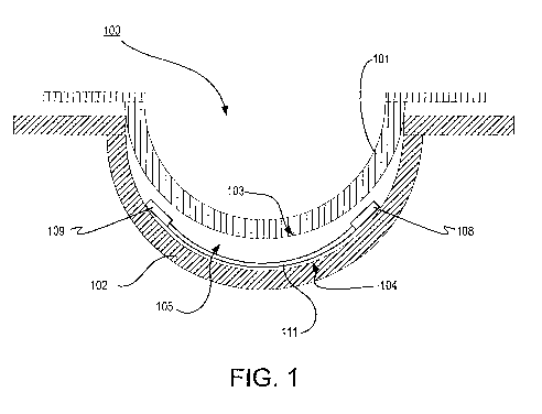
Referring now to Fig. 1, a diagram of a mold device 100 for an ophthalmic lens
is illustrated with a Media Insert 111. As used herein, the terms a mold
device 100
includes a plastic formed to shape a cavity 105 into which a lens forming
mixture can
be dispensed such that upon reaction or cure of the lens forming mixture, an
7
CA 02862666 2014-07-24
WO 2013/112862 PCT/US2013/023182
ophthalmic lens of a desired shape is produced. The molds and mold assemblies
100
of this invention are made up of more than one "mold parts" or "mold pieces"
101-102.
The mold parts 101-102 can be brought together such that a cavity 105 is
formed
between the mold parts 101-102 in which a lens can be formed. This combination
of
mold parts 101-102 is preferably temporary. Upon formation of the lens, the
mold
parts 101-102 can again be separated for removal of the lens.
At least one mold part 101-102 has at least a portion of its surface 103-104
in
contact with the lens forming mixture such that upon reaction or cure of the
lens
forming mixture that surface 103-104 provides a desired shape and form to the
portion
of the lens with which it is in contact. The same is true of at least one
other mold part
101-102.
Thus, for example, a mold device 100 is formed from two parts 101-102, a
female concave piece (front piece) 102 and a male convex piece (back piece)
101 with
a cavity formed between them. The portion of the concave surface 104 which
makes
contact with lens forming mixture has the curvature of the front curve of an
ophthalmic
lens to be produced in the mold device 100 and is sufficiently smooth and
formed such
that the surface of an ophthalmic lens formed by polymerization of the lens
forming
mixture which is in contact with the concave surface 104 is optically
acceptable.
The front mold piece 102 may also have an annular flange integral with and
surrounding circular circumferential edge and extends from it in a plane
normal to the
axis and extending from the flange (not shown).
A lens forming surface can include a surface 103-104 with an optical quality
surface finish, which indicates that it is sufficiently smooth and formed so
that a lens
surface fashioned by the polymerization of a lens forming material in contact
with the
molding surface is optically acceptable. Furtherõ the lens forming surface 103-
104
may have a geometry that is necessary to impart to the lens surface the
desired optical
characteristics, including without limitation, spherical, aspherical and
cylinder power,
wave front aberration correction, corneal topography correction and the like
as well as
any combinations thereof.
At 111, a Media Insert is illustrated onto which an Energy Source 109 and a
Component 108 are mounted. The Media Insert 111 may be any receiving material
onto which an Energy Source 109 may be placed, may also include circuit paths,
components and other aspects useful to place the Energy Source109 in
electrical
8
CA 02862666 2014-07-24
WO 2013/112862 PCT/US2013/023182
communication with the Component 108 and enable the Component to draw an
electrical current from the Energy Source 109.
The Media Insert 111 may include a flexible substrate. Additional examples
can include a Media Insert 111 that is rigid, such as a silicon wafer. A rigid
insert may
include an optical zone providing an optical property (such as those utilized
for vision
correction) and a non-optical zone portion. An Energy Source can be placed on
one or
both of the optic zone and non-optic zone of the insert. Still other examples
can
include an annular insert, either rigid or formable or some shape which
circumvents an
optic zone through which a user sees.
Other examples include a Media Insert 111 formed of a clear coat of a material
which be incorporated into a lens when the lens is formed. The clear coat can
include
for example a pigment as described below, a monomer or other biocompatible
material.
An Energy Source 109 may be placed onto Media Insert 111 prior to placement
of the Media Insert 111 into a mold portion used to form a lens. The Media
Insert 111
may also include one or more components which will receive an electrical
charge via
the Energy Source 109.
A lens with a Media Insert 111 can include a rigid center soft skirt design in
which a central rigid optical element is in direct contact with the atmosphere
and the
corneal surface on respective an anterior and posterior surfaces, wherein the
soft skirt
of lens material (typically a hydrogel material) is attached to a periphery of
the rigid
optical element and the rigid optical element also acts as a Media Insert
providing
energy and functionality to the resulting ophthalmic lens.
Some examples include a Media Insert 111 that is a rigid lens insert fully
encapsulated within a hydrogel matrix. A Media Insert 111 which is a rigid
lens insert
may be manufactured, for example using microinjection molding technology. For
example, a poly(4-methylpent- 1 -ene copolymer resin with a diameter of
between about
6mm to lOmm and a front surface radius of between about 6 mm and lOmm and a
rear
surface radius of between about 6 mm and 10 mm and a center thickness of
between
about 0.050mm and 0.5 mm, may be included. An insert with a diameter of about
8.9
mm and a front surface radius of about 7.9 mm and a rear surface radius of
about 7.8
mm and a center thickness of about 0.100 mm and an edge profile of about 0.050
9
CA 02862666 2014-07-24
WO 2013/112862 PCT/US2013/023182
radius may be included. A micromolding machine may include the Microsystem 50
five-ton system offered by Battenfield Inc.
The Media Insert can be placed in a mold part 101-102 utilized to form an
ophthalmic lens.
Mold part 101-102 material can include, for example: a polyolefin of one or
more of: polypropylene, polystyrene, polyethylene, polymethyl methacrylate,
and
modified polyolefins. Other molds can include a ceramic or metallic material.
Other mold materials that may be combined with one or more additives to form
an ophthalmic lens mold include, for example, Zieglar-Natta polypropylene
resins
(sometimes referred to as znPP); a clarified random copolymers for clean
molding as
per FDA regulation 21 CFR (c) 3.2; a random copolymer (znPP) with ethylene
group.
Still further, the molds may contain polymers such as polypropylene,
polyethylene, polystyrene, polymethyl methacrylate, modified polyolefins
containing
an alicyclic moiety in the main chain and cyclic polyolefins. This blend can
be used
on either or both mold halves, where it is preferred that this blend is used
on the back
curve and the front curve consists of the alicyclic co-polymers.
In some preferred methods of making molds 100, injection molding is utilized
according to known techniques, however, methods can also include molds
fashioned
by other techniques including, for example: lathing, diamond turning, or laser
cutting.
Typically, lenses are formed on at least one surface of both mold parts 101-
102.
However, one surface of a lens may be formed from a mold part 101-102 and
another
surface of a lens can be formed using a lathing method, or other methods.
Lenses
Referring now to Fig. 2A-2D, exemplary designs of Media Inserts 211-214 are
illustrated. Fig. 2A illustrates an annular Media Insert 211. Other Media
Inserts may
be of various shapes conducive to placement with an ophthalmic lens. Some
preferred
shapes include shapes with arcuate designs matching a portion of the overall
shape of
the ophthalmic lens. Fig. 2B illustrates a Media Insert 212 which includes an
area of
about 1/2 of an full annular design and also includes an arcuate area which
may
surround an optic zone of a lens into which the Media Insert 212 is placed.
Similarly,
Fig. 2C includes a Media insert 213 of about 1/3 of an annular design. Fig. 2D
illustrates an annular design 214 with multiple discrete portions 215, 216, 21
of the
CA 02862666 2014-07-24
WO 2013/112862 PCT/US2013/023182
Media Insert 214. Discrete portions 215, 216, 21 can be useful to isolate
various
functions attributed to the individual portions 215, 216, 21. For example, one
discrete
portion 215, 216, 21 may contain one or more Energy Sources and another
discrete
portion 215, 216, 21 may include components.
A Media Insert 211-214 may optionally have an optic zone that includes a
variable optic powered by an Energy Source located on the Media Insert 211-
214. The
Media Insert 211-214 can also include circuitry to control the variable optic
included
in the optic zone 211-214. In this discussion, a variable optic can be
considered a
component.
An Energy Source can be in electrical communication with a component. The
component can include any device which responds to an electrical charge with a
change in state, such as, for example: a semiconductor type chip; a passive
electrical
device; or an optical device such as a crystal lens.
An Energy Source includes, for example: battery or other electrochemical cell;
capacitor; ultracapacitor; supercapacitor; or other storage component. A
lithium ion
battery may be located on a Media Insert 211-214 on the periphery of an
ophthalmic
lens outside of the optic zone and chargeable via one or more of radio
frequency and
magnetic inductance into an Energy Source deposited via ink jetting.
A preferred lens type can include a lens that includes a silicone containing
component. A "silicone-containing component" is one that contains at least one
[-Si-
0-] unit in a monomer, macromer or prepolymer. Preferably, the total Si and
attached
0 are present in the silicone-containing component in an amount greater than
about 20
weight percent, and more preferably greater than 30 weight percent of the
total
molecular weight of the silicone-containing component. Useful silicone-
containing
components preferably comprise polymerizable functional groups such as
acrylate,
methacrylate, acrylamide, methacrylamide, vinyl, N-vinyl lactam, N-vinylamide,
and
styryl functional groups.
Suitable silicone containing components include compounds of Formula I
R1 R1 R1
I I 1
R1-Si-O-Si-O-Si-R1
1 1 1
F11
R1
30 -
11
CA 02862666 2014-07-24
WO 2013/112862 PCT/US2013/023182
where
Rl is independently selected from monovalent reactive groups, monovalent
alkyl groups, or monovalent aryl groups, any of the foregoing which may
further
comprise functionality selected from hydroxy, amino, oxa, carboxy, alkyl
carboxy,
alkoxy, amido, carbamate, carbonate, halogen or combinations thereof; and
monovalent siloxane chains comprising 1-100 Si-0 repeat units which may
further
comprise functionality selected from alkyl, hydroxy, amino, oxa, carboxy,
alkyl
carboxy, alkoxy, amido, carbamate, halogen or combinations thereof
where b = 0 to 500, where it is understood that when b is other than 0, b is a
distribution having a mode equal to a stated value; wherein at least one Rl
comprises a
monovalent reactive group, and in some examples between one and 3 Rl comprise
monovalent reactive groups.
As used herein "monovalent reactive groups" are groups that can undergo free
radical and/or cationic polymerization. Non-limiting examples of free radical
reactive
groups include (meth)acrylates, styryls, vinyls, vinyl ethers,
Ci_6alkyl(meth)acrylates,
(meth)acrylamides, Ci_6alkyl(meth)acrylamides, N-vinyllactams, N-vinylamides,
C2_12alkenyls, C2_12alkenylphenyls, C2_12alkenylnaphthyls,
C2_6alkenylpheny1C1_6alkyls,
0-vinylcarbamates and 0-vinylcarbonates. Non-limiting examples of cationic
reactive
groups include vinyl ethers or epoxide groups and mixtures thereof. In one
embodiment the free radical reactive groups comprises (meth)acrylate,
acryloxy,
(meth)acrylamide, and mixtures thereof
Suitable monovalent alkyl and aryl groups include unsubstituted monovalent Ci
to Ci6alkyl groups, C6-C14 aryl groups, such as substituted and unsubstituted
methyl,
ethyl, propyl, butyl, 2-hydroxypropyl, propoxypropyl, polyethyleneoxypropyl,
combinations thereof and the like.
In one example b is zero, one Ri is a monovalent reactive group, and at least
3
Ri are selected from monovalent alkyl groups having one to 16 carbon atoms,
and in
another example from monovalent alkyl groups having one to 6 carbon atoms. Non-
limiting examples of silicone components include 2-methyl-,2-hydroxy-3-[3-
[1,3,3,3-
tetramethyl-l-[(trimethylsily1)oxy]disiloxanyl]propoxy]propyl ester ("SiGMA"),
2-hydroxy-3-methacryloxypropyloxypropyl-tris(trimethylsiloxy)silane,
3 -methacryloxypropyltris(trimethylsiloxy)silane ("TRIS"),
3-methacryloxypropylbis(trimethylsiloxy)methylsilane and
12
CA 02862666 2014-07-24
WO 2013/112862 PCT/US2013/023182
3 -methacryloxypropylp entamethyl disiloxane.
In another example, b is 2 to 20, 3 to 15 or 3 to 10; at least one terminal Rl
comprises a monovalent reactive group and the remaining Rl are selected from
monovalent alkyl groups having 1 to 16 carbon atoms, and in another example
from
monovalent alkyl groups having 1 to 6 carbon atoms. In yet another example, b
is 3 to
15, one terminal Rl comprises a monovalent reactive group, the other terminal
Rl
comprises a monovalent alkyl group having 1 to 6 carbon atoms and the
remaining Rl
comprise monovalent alkyl group having 1 to 3 carbon atoms. Non-limiting
examples
of silicone components include (mono-(2-hydroxy-3-methacryloxypropy1)-propyl
ether
terminated polydimethylsiloxane (400-1000 MW)) ("OH-mPDMS"),
monomethacryloxypropyl terminated mono-n-butyl terminated
polydimethylsiloxanes
(800-1000 MW), ("mPDMS").
In another example b is 5 to 400 or from 10 to 300, both terminal Rl comprise
monovalent reactive groups and the remaining Rl are independently selected
from
monovalent alkyl groups having 1 to 18 carbon atoms which may have ether
linkages
between carbon atoms and may further comprise halogen.
In one example, where a silicone hydrogel lens is desired, the lens will be
made
from a reactive mixture comprising at least about 20 and preferably between
about 20
and 70%wt silicone containing components based on total weight of reactive
monomer
components from which the polymer is made.
In another example, one to four Rl comprises a vinyl carbonate or carbamate of
the formula:
Formula II
R 0
1 II
H2C=C-(CH2)q-0-C-Y
wherein: Y denotes 0-, S- or NH-;
R denotes, hydrogen or methyl; d is 1, 2, 3 or 4; and q is 0 or 1.
The silicone-containing vinyl carbonate or vinyl carbamate monomers
specifically include: 1,3 -bis[4-(vinyloxycarbonyloxy)but-1-yl]tetramethyl-
disiloxane;
3 -(vinyloxyc arbonylthio) propyl-[tris (trimethylsiloxy)silane]; 3-
[tris(trimethylsiloxy)silyl] propyl allyl carbamate; 3-
[tris(trimethylsiloxy)silyl] propyl
13
CA 02862666 2014-07-24
WO 2013/112862 PCT/US2013/023182
vinyl carbamate; trimethylsilylethyl vinyl carbonate; trimethylsilylmethyl
vinyl
carbonate, and
0
CH3 CH3 CH3 0
11 I I I II
H2C=C¨OCO(CH3)4¨Si 0 ___________ Si ¨O ___ Si (CH2)4000¨C=CH2
H
1 1 1 H
CH3 CH3 CH3
- -25
Where biomedical devices with modulus below about 200 are desired, only one
Rl shall comprise a monovalent reactive group and no more than two of the
remaining
Rl groups will comprise monovalent siloxane groups.
Another class of silicone-containing components includes polyurethane
macromers of the following formulae:
Formulae IV-VI
(*D*A*D*G), *D*D*El;
E(*D*G*D*A), *D*G*D*E1 or;
E(*D*A*D*G), *D*A*D*E1
wherein:
D denotes an alkyl diradical, an alkyl cycloalkyl diradical, a cycloalkyl
diradical, an aryl diradical or an alkylaryl diradical having 6 to 30 carbon
atoms,
G denotes an alkyl diradical, a cycloalkyl diradical, an alkyl cycloalkyl
diradical, an aryl diradical or an alkylaryl diradical having 1 to 40 carbon
atoms and
which may contain ether, thio or amine linkages in the main chain;
* denotes a urethane or ureido linkage;
a is at least 1;
A denotes a divalent polymeric radical of formula:
Formula VII
-R1 I- R11
I I
-(C H2 )y-S i 0 -S i-(C H2 )y-
11 1 k 1
- -p
RH independently denotes an alkyl or fluoro-substituted alkyl group having 1
to10
carbon atoms which may contain ether linkages between carbon atoms; y is at
least 1;
14
CA 02862666 2014-07-24
WO 2013/112862 PCT/US2013/023182
and p provides a moiety weight of 400 to 10,000; each of E and E1
independently
denotes a polymerizable unsaturated organic radical represented by formula:
Formula VIII
R12
R13CH=C¨(CH2)w¨(X)x¨(Z)z¨(Ar)y¨R14¨
wherein: R12 is hydrogen or methyl; R13 is hydrogen, an alkyl radical having 1
to 6
carbon atoms, or a ¨CO--Y--R'5 radical wherein Y is ¨0¨,Y¨S¨ or ¨NH¨;
R14 is a divalent radical having 1 to 12 carbon atoms; X denotes ¨CO¨ or
¨000¨;
Z denotes ¨0¨ or ¨NH¨; Ar denotes an aromatic radical having 6 to 30 carbon
atoms; w is 0 to 6; x is 0 or 1; y is 0 or 1; and z is 0 or 1.
A preferred silicone-containing component is a polyurethane macromer
represented by the following formula:
Formula IX
cH3
11 11 11 11
at=c-(3=c-ocN-R16-NcccH2cH2ocH2cH2ocN- R16- I H FO(CH2)m(SO)Si¨ (CH2)n, OCN-
R16- NCCCH2CH2OCH2CH2OCN¨ R NCO¨CH2CH2030 CH2
I l I
CHYH33 CY:33 H H H H
a
wherein R16 is a diradical of a diisocyanate after removal of the isocyanate
group, such
as the diradical of isophorone diisocyanate. Another suitable silicone
containing
macromer is compound of formula X (in which x + y is a number in the range of
10 to
30) formed by the reaction of fluoroether, hydroxy-terminated
polydimethylsiloxane,
isophorone diisocyanate and isocyanatoethylmethacrylate.
Formula X
0 0
)t 0
-,'y "----"Nu'it-O(SA4e2O)25SR\4e20 NH )1,
0 N.
OCH2CF2¨(0CF2)x¨(0CF2CF2)y¨OCF2C1120
NHI..-0(SRVIe20)25SA4e2.0)- NH
0 NH
Other silicone containing components suitable for use in this invention
include
macromers containing polysiloxane, polyalkylene ether, diisocyanate,
polyfluorinated
hydrocarbon, polyfluorinated ether and polysaccharide groups; polysiloxanes
with a
polar fluorinated graft or side group having a hydrogen atom attached to a
terminal
CA 02862666 2014-07-24
WO 2013/112862 PCT/US2013/023182
difluoro-substituted carbon atom; hydrophilic siloxanyl methacrylates
containing ether
and siloxanyl linkanges and crosslinkable monomers containing polyether and
polysiloxanyl groups. Any of the foregoing polysiloxanes can also be used as
the
silicone containing component in this invention.
Processes
The following method steps are provided as examples of processes that may be
implemented according to some aspects of the present invention. It should be
understood that the order in which the method steps are presented is not meant
to be
limiting and other orders may be used to implement the invention. In addition,
not all
of the steps are required to implement the present invention and additional
steps may
be included in various examples of the present invention.
Referring now to Fig. 4, a flowchart illustrates steps that may be used to
implement the present invention, at 401 an Energy Source is placed on to a
Media
Insert. The Media Insert may or may not also contain one or more components.
At 402, a reactive monomer mix can be deposited into a first mold part.
At 403, the Media Insert is placed into a cavity formed by the first mold
part.
The Media Insert 111 may be placed in the mold part 101-102 via mechanical
placement. Mechanical placement can include, for example, a robot or other
automation, such as those known in the industry to place surface mount
components.
Human placement of a Media Insert 111 is also within the scope of the present
invention. Accordingly, any mechanical placement effective to place a Media
Insert
111 with an Energy Source 109 within a cast mold part such that the
polymerization of
a Reactive Mixture 110 contained by the mold part will include the Energy
Source 109
in a resultant ophthalmic lens.
A processor device, MEMS, NEMS or other component may also be mounted
on the Media Insert and be in electrical communication with the Energy Source.
At 404, the first mold part can be placed proximate to the second mold part to
form a lens forming cavity with at least some of the reactive monomer mix and
the
Energy Source in the cavity. At 405, the reactive monomer mix within the
cavity can
be polymerized. Polymerization can be accomplished for example via exposure to
one
or both of actinic radiation and heat. At 406, the lens is removed from the
mold parts.
16
CA 02862666 2014-07-24
WO 2013/112862 PCT/US2013/023182
Although invention may be used to provide hard or soft contact lenses made of
any known lens material, or material suitable for manufacturing such lenses,
preferably, the lenses of the invention are soft contact lenses having water
contents of
about 0 to about 90 percent. More preferably, the lenses are made of monomers
containing hydroxy groups, carboxyl groups, or both or be made from silicone-
containing polymers, such as siloxanes, hydrogels, silicone hydrogels, and
combinations thereof. Material useful for forming the lenses of the invention
may be
made by reacting blends of macromers, monomers, and combinations thereof along
with additives such as polymerization initiators. Suitable materials include,
without
limitation, silicone hydrogels made from silicone macromers and hydrophilic
monomers.
Referring now again to Fig 4, at 402, a reactive mixture is placed between a
first
mold part and a second mold part and at 403, the Media Insert is positioned in
contact
with the reactive mixture. At 404, the first mold part is placed proximate to
a second
mold part to form a lens cavity with the reactive monomer mix and the media in
the
lens cavity.
At 405, the reactive mixture is polymerized, such as for example via exposure
to
one or both of actinic radiation and heat. At 406, an ophthalmic device
incorporating
the Media Insert and Energy Source is removed from the mold parts used to form
the
ophthalmic device.
Referring now to Fig. 5, in another aspect of the present invention, a Media
Insert
incorporated into an ophthalmic device can be powered via an incorporated
Energy
Source. At 501, a Media Insert is placed within an ophthalmic lens, as
discussed
above. At 502, the Media Insert is placed in electrical communication with a
component incorporated into the Media Insert or otherwise included in the
ophthalmic
lens 105. Electrical communication can be accomplished, for example, via
circuitry
incorporated into the Media Insert or via pathways iffl( jetted or otherwise
formed
directly upon lens material.
At 503, energy is directed to a component incorporated into the ophthalmic
lens.
The energy can be directed, for example, via electrical circuitry capable of
conducting
the electrical charge. At 504 the component performs some action based upon
the
energy directed to the component. The action can include a mechanical action
17
CA 02862666 2014-07-24
WO 2013/112862 PCT/US2013/023182
affecting the lens or some action processing information including one or more
of:
receiving, transmitting, storing and manipulating information. Examples will
include
the information being processed and stored as digital values.
At 505, information may be transmitted from a component incorporated into the
lens.
Apparatus
Referring now to Fig. 3, automated apparatus 310 is illustrated with one or
Media Insert 314 transfer interfaces 311. As illustrated, multiple mold parts,
each with
an associated Media Insert 314 are contained on a pallet 313 and presented to
a media
transfer interfaces 311. Examples may include a single interface individually
placing
Media Inserts 314, or multiple interfaces (not shown) simultaneously placing
Media
Inserts 314 in multiple mold parts, and in some examples, in each mold.
Another aspect includes an apparatus to support the Media Insert 314 while the
body of the ophthalmic lens is molded around these components. The Energy
Source
may be affixed to holding points in a lens mold (not illustrated). The holding
points
may be affixed with polymerized material of the same type that will be formed
into the
lens body.
Referring now to Fig. 6 a controller 600 is illustrated that may be used in
some
examples of the present invention. The controller 600 includes one or more
processors
610, which may include one or more processor components coupled to a
communication device 620. In some examples, a controller 600 can be used to
transmit energy to the Energy Source placed in the ophthalmic lens.
The processors 610 are coupled to a communication device configured to
communicate energy via a communication channel. The communication device may
be used to electronically control one or more of: automation used in the
placement of a
media with an Energy Source into the ophthalmic lens mold part and the
transfer of
digital data to and from a component mounted on the media and placed within an
ophthalmic lens mold part or to control a component incorporated into the
ophthalmic
lens.
The communication device 620 may also be used to communicate, for example,
with one or more controller apparatus or manufacturing equipment components.
18
CA 02862666 2014-07-24
WO 2013/112862 PCT/US2013/023182
The processor 610 is also in communication with a storage device 630. The
storage device 630 may comprise any appropriate information storage device,
including combinations of magnetic storage devices (e.g., magnetic tape and
hard disk
drives), optical storage devices, and/or semiconductor memory devices such as
Random Access Memory (RAM) devices and Read Only Memory (ROM) devices.
The storage device 630 can store a program 640 for controlling the processor
610. The processor 610 performs instructions of a software program 640, and
thereby
operates in accordance with the present invention. For example, the processor
610
may receive information descriptive of Media Insert placement, component
placement,
and the like. The storage device 630 can also store ophthalmic related data in
one or
more databases 650 and 660. The database may include customized Media Insert
designs, metrology data, and specific control sequences for controlling energy
to and
from a Media Insert.
Referring to Fig. 7, a top down depiction of a Media Insert 700 is shown. In
this depiction, an Energy Source 710 is shown in a periphery portion 711 of
the Media
Insert 700. The Energy Source 710 may include, for example, a thin film,
rechargeable
lithium ion battery. The Energy Source 710 may be connected to contact points
714 to
allow for interconnection. Wires may be wire bound to the contact points 714
and
connect the Energy Source 710 to a photoelectric cell 715 which may be used to
reenergize the battery Energy Source 710. Additional wires may connect the
Energy
Source 710 to a flexible circuit interconnect via wire bonded contact.
The Media Insert 700 may include a flexible substrate. This flexible substrate
may be formed into a shape approximating a typical lens form in a similar
manner
previously discussed. However to add additional flexibility, the Media Insert
700 may
include additional shape features such as radial cuts along its length.
Various
electronic components 712 such as integrated circuits, discrete components,
passive
components and such devices may also be included.
An optic zone 713 is also illustrated. The optic zone may be optically passive
with no optical change, or it may have a predetermined optical characteristic,
such as a
predefined optical correction. Still other examples lenses include an optical
zone with
a variable optic component that may be varied on command.
19
CA 02862666 2014-07-24
WO 2013/112862 PCT/US2013/023182
Referring now to Fig. 8, a cross sectional of a Media Insert 800 is
illustrated.
The Media Insert 800 can include an optic zone 830 as discussed above and also
one or
more periphery portions 810-820. The media insert and components may be placed
within the periphery portions 810-820.
In some examples there may be manners of affecting the ophthalmic lens'
appearance. Aesthetics of the thin film microbattery surface may be altered in
various
manners which demonstrate a particular appearance when embedded in the
electroactive contact lens or shaped hydrogel article. For example, the thin
film
microbattery may be produced with aesthetically pleasing patterned and/or
colored
packaging materials which could serve to either give a muted appearance of the
thin
film microbattery or alternatively provide iris-like colored patterns, solid
and/or mixed
color patterns, reflective designs, iridescent designs, metallic designs, or
potentially
any other artistic design or pattern. In other examples, the thin film battery
may be
partially obscured by other components within the lens, for example a
photovoltaic
chip mounted to the battery anterior surface, or alternatively placement of
the battery
behind all or a portion of a flexible circuit. Furthermore, the thin film
battery may be
strategically located such that either the upper or lower eyelid partially or
wholly
obscures the visibility of the battery. It may be apparent to one skilled in
the art that
there are numerous examples relating to the appearance of an energized
ophthalmic
device and the methods to define them.
There may be numerous examples relating to the method of forming an
energized ophthalmic device of the various types that have been described. In
one set
of examples, described herein may include assembling subcomponents of a
particular
energized ophthalmic lens in separate steps. The
"off-line" assembly of
advantageously shaped thin film microbatteries, flexible circuits,
interconnects,
microelectronic components, and/or other electroactive components in
conjunction
with a biocompatible, inert, conformal coating to provide an all-inclusive,
embeddable
singular package that can be simply incorporated into standard contact lens
manufacturing processes. Flexible circuits may include those fabricated from
copper
clad polyimide film or other similar substrates. Conformal coatings may
include, but
are not limited to, parylene (grades N, C, D, HT, and any combinations
thereof),
poly(p-xylylene), dielectric coatings, silicone conformal coatings, or any
other
advantageous biocompatible coatings.
CA 02862666 2014-07-24
WO 2013/112862 PCT/US2013/023182
Some examples of the present invention may be methods that are directed
toward the geometric design of thin film microbatteries in geometries amenable
to the
embedment within and/or encapsulation by ophthalmic lens materials. Other
examples
may involve methods that incorporate thin film microbatteries in various
materials
such as, but not limited to, hydrogels, silicone hydrogels, rigid gas-
permeable "RGP"
contact lens materials, silicones, thermoplastic polymers, thermoplastic
elastomers,
thermosetting polymers, conformal dielectric/insulating coatings, and hermetic
barrier
coatings.
Other examples may involve methods for the strategic placement of an Energy
Source within an ophthalmic lens geometry. Specifically, the Energy Source may
be
an opaque article. Since the Energy Source may not obstruct the transmission
of light
through the ophthalmic lens, methods of design may ensure that the central 5-8
mm of
the contact lens may not be obstructed by any opaque portions of the Energy
Source.
It may be apparent to one skilled in the art that there may be many different
embodiments relating to the design of various Energy Sources to interact
favorably
with the optically relevant portions of the ophthalmic lens.
The mass and density of the Energy Source may facilitate designs such that
said Energy Source may also function either alone or in conjunction with other
lens
stabilization zones designed into the body of the ophthalmic lens to
rotationally
stabilize the lens while on eye. Such examples could be advantageous for a
number of
applications including, but not limited to, correction of astigmatism,
improved on-eye
comfort, or consistent/controlled location of other components within the
energized
ophthalmic lens.
In addition, the Energy Source may be placed a certain distance from the outer
edge of the contact lens to enable advantageous design of the contact lens
edge profile
in order to provide good comfort while minimizing occurrence of adverse
events.
Examples of such adverse events to be avoided may include superior epithelial
arcuate
lesions or giant papillary conjunctivitis.
By way of non-limiting example, a cathode, electrolyte and anode features of
embedded electrochemical cells may be formed by printed appropriate inks in
shapes
to define such cathode, electrolyte and anode regions. It may be apparent that
batteries
thus formed could include both single use cells, based for example on
manganese
21
CA 02862666 2014-07-24
WO 2013/112862 PCT/US2013/023182
oxide and zinc chemistries, and rechargeable thin batteries based on lithium
chemistry
similar to the above mentioned thin film battery chemistry. It may be apparent
to one
skilled in the arts that a variety of different examples of the various
features and
methods of forming energized ophthalmic lenses may involve the use of printing
techniques.
In addition, energy harvesters may be included and placed in electrical
communication in a fashion which enables the energy harvesters to charge one
or more
Energy Sources. Energy harvesters can include, for example: photovoltaic
energy
cells, thermoelectric cells or piezoelectric cells. Harvesters have a positive
aspect in
that they can absorb energy from the environment and then can provide
electrical
energy without an external wired connection. Harvesters may comprise an energy
source in an energized ophthalmic lens. However, the energy harvester may be
combined with other sources that can store energy in an electrical form.
Other types of Energy Source include the use of capacitor type devices. It may
be apparent, that capacitors may provide an energy density solution that is
higher than
energy harvesters but less than that of batteries.
Capacitors are a type of Energy Source that stores energy in an electrical
form
and therefore, may be one of the Energy Sources that can be combined with
energy
harvesters to create a wireless Energy Source that is capable of storage of
energy.
Generally capacitors have an advantage over batteries in that they have higher
power
density, in general, than batteries. There are many different types of
capacitors ranging
from standard electrical thin film capacitors, Mylar capacitors, electrolytic
capacitors
and relative newer and more advanced technologies of high-density nanoscale
capacitors or supercapacitors.
Additionally, Energy Sources including electrochemical cells or batteries may
define a relatively desirable operational point. Batteries have numerous
advantageous
characteristics. For example, batteries store energy in a form that is
directly converted
to electrical energy. Some batteries may be rechargeable or Re-energizable and
therefore, represent another category of Energy Source that may be coupled to
energy
harvesters. Batteries generally are capable of relatively high energy density,
and the
energy batteries store can perform functions with relatively higher energy
requirements
as compared with other miniaturized Energy Sources. In addition, the batteries
can be
22
CA 02862666 2014-07-24
WO 2013/112862 PCT/US2013/023182
assembled into forms that are flexible. For applications requiring high power
capabilities, it may be apparent to one skilled in the art that a Battery may
also be
coupled to Capacitors. There may be numerous embodiments that comprise a
battery
at least as part of an Energy Source in an energized ophthalmic lens.
A fuel cell may be included as an Energy Source. Fuel cells generate
electricity
by consuming a chemical fuel source which then generates electricity and
byproducts
including heat energy. Fuel cell Energy Sources may be possible using
biologically
available materials as the fuel source.
There are many different types of batteries which may be included in energized
ophthalmic lenses. For example, single use batteries may be formed from
various
cathode and anode materials. By way of non-limiting examples these materials
may
include one or more of: Zinc, carbon, Silver, Manganese, Cobalt, Lithium and
Silicon.
Still other examples may derive from the use of batteries that are
rechargeable. Such
batteries may in turn be made of one or more of: Lithium Ion technology;
Silver
Technology; Magnesium technology; Niobium technology or other current
providing
material. It may be apparent to one skilled in the art that various current
battery
technologies for single use or rechargeable battery systems may comprise the
Energy
Source of an energized ophthalmic lens.
The physical and dimensional constraints of a contact lens environment may be
conducive to thin film batteries. Thin film batteries may occupy the small
volume of
space consistent with human ophthalmic examples. Furthermore, they may be
formed
upon a substrate that is flexible allowing for the body of both the ophthalmic
lens and
included battery with substrate to have freedom to flex.
In the case of thin film batteries, examples may include single charge and
rechargeable forms. Rechargeable batteries afford the ability of extended
usable
product lifetime and, therefore, higher energy consumption rates. Much
development
activity has focused on the technology to produce electrically energized
ophthalmic
lenses with rechargeable thin film batteries; however, the invention is not
limited to
this subclass.
Rechargeable thin film batteries are commercially available, for example, Oak
Ridge National Laboratory has produced various forms since the early 1990s.
Current
commercial producers of such batteries include Excellatron Solid State, LLC
(Atlanta,
23
CA 02862666 2014-07-24
WO 2013/112862 PCT/US2013/023182
GA), Infinite Power Solutions (Littleton, CO), and Cymbet Corporation, (Elk
River,
MN). The technology is currently dominated by uses that include flat thin film
batteries. Use of such batteries may comprise forming the thin film battery
into a three
dimensional shape, for example with a spherical radius of curvature. Numerous
shapes
and forms of such a three dimensional battery are within the scope of the
invention.
Stacked Integrated Component Media Inserts
The thin film batteries and/or the energized electronic elements may be
included into the media insert in the form of stacked integrated components.
Proceeding to Fig. 9, item 900, an illustration of a cross section of this
type is provided
in a non-limiting example. The media insert may include numerous layers of
different
types which are encapsulated into forms consistent with the ophthalmic
environment
that they will occupy. These inserts with stacked integrated component layers
may
assume the entire insert shapes as depicted in the various exemplary shapes in
Fig 2A,
2B, 2C and 2D. Alternatively in some cases, the media insert may assume these
shapes whereas the stacked integrated component may occupy just a portion of
the
volume within the entire shape.
Continuing with the example of item 900, a stacked integrated component
media insert may assume numerous functional aspects. As shown in Fig. 9, the
thin
film batteries, may comprise one or more of the layers that are stacked upon
each
other, in this case layers 906 and 907 may represent the battery layers, with
multiple
components in the layers. One such battery component may be found as item 940.
As
can be seen in nearly all of the layers, there may be interconnections that
are made
between two layers that are stacked upon each other. In the state of the art
there may
be numerous manners to make these interconnections, however as demonstrated by
items 930 and 931, the interconnection may be made through solder ball
interconnections between the layers 907 and 908. In some cases only these
connections may be required, however in other cases the solder balls may
contact other
interconnection elements, as for example with through layer vias. In the
component in
layer 907 which has interconnections 930 and 931, there may be a through
substrate
via in the body of the thin film battery component that passes electrical
connection
from one side of the component to another side. Some of these thru substrate
24
CA 02862666 2014-07-24
WO 2013/112862 PCT/US2013/023182
components may then, on the alternative side of the substrate, make another
interlayer
connection to a layer above the component, as may be the case for component
940.
In other layers of the Stacked Integrated Component media insert, a layer
dedicated to interconnection of various components in the interconnect layers
may be
found, as for example layer 905. This layer may contain vias and routing lines
that
pass signals from various components to others. For example, 905 may provide
the
various battery elements connections to a power management unit that may be
present
in the technology layer components of layer 904. As well the interconnection
layer
may make connections between components in the technology layer and also
components outside the technology layer; as may exist for example in the
Integrated
Passive Device component shown as item 920. There may be numerous manners that
routing of electrical signals may be supported by the presence of dedicated
interconnect layers.
There are two features identified as technology layers, items 904 and 902.
These features represent a diversity of technology options that may be
included in
media inserts. One of the layers may include CMOS, BiCMOS, Bipolar, or memory
based technologies whereas the other layer may include a different technology.
Alternatively, the two layers may represent different technology families
within a same
overall family; as for example layer 902 may include electronic elements
produced
using a 0.5 micron CMOS technology and layer 904 may include elements produced
using a 20 nanometer CMOS technology. It may be apparent that many other
combinations of various electronic technology types would be consistent within
the art
described herein.
Additional interconnection layers similar to layer 905 may be present. The
additional layer may be another full layer of interconnection as depicted in
item 903.
Alternatively, the additional layer may be a portion of a stacked layer as
shown in item
910. In some cases these additional elements may provide electrical
interconnection,
in others there may be structural interconnection performed by the presence of
the
layer. Both structural and electronic interconnection may be included between
the
various layers.
The media insert may include locations for electrical interconnections to
components outside the insert as has been described previously. In other
examples,
CA 02862666 2014-07-24
WO 2013/112862 PCT/US2013/023182
however the media insert may also include interconnection to external
components in a
wireless manner. In such cases, the use of antennas may provide exemplary
manners
of wireless communication. A layer may exist, as shown as item 901, where such
an
exemplary antenna may be supported in the layer. In many cases, such an
antenna
layer may be located on the top or bottom of the stacked integrated component
device
within the media insert. As shown in item 908, it is possible for such a layer
on the top
or bottom to also not include an antenna for wireless communication and
therefore act
as a supporting substrate upon which the stacked device is produced.
In some of the examples discussed herein, the battery elements may be
included as elements in at least one of the stacked layers themselves. It may
be noted
as well that other embodiments may be possible where the battery elements are
located
externally to the stacked integrated component layers. Still further a
separate battery
or other energization component may also exist within the media insert, or
alternatively these separate energization components may also be located
externally to
the media insert.
Proceeding to Fig. 10, item 1000, a stacked integrated component media insert,
item 1040, within an ophthalmic lens, item 1030, is depicted. The boundary of
the
media insert material is depicted by the feature labeled 1040. Within the
bounds of
the media insert, in this example, is located stacked integrated component
layers
depicted as item 1010. In some examples of this type, external to the media
insert but
within the ophthalmic lens, 1030, an electro active lens may be represented as
item
1020. The control signals for the components within the lens may originate
from a
wireless signal as discussed earlier. And, the stacked component layers within
the
media insert may receive this wireless signal and in some cases adjust an
electrical
signal that is routed on wires that run externally to the media insert, 1040,
connecting
to the electroactive lens 1020. It may be apparent that there may be many
alternatives
to using and connecting a media insert which contains stacked integrated
components
within an ophthalmic lens and that may include stacked integrated components
in
devices other than ophthalmic lenses as well including in a non-limiting
sense,
energized biomedical devices of various kinds.
Various examples and aspects of the present invention are described below.
26
CA 02862666 2014-07-24
WO 2013/112862 PCT/US2013/023182
A method of forming a stacked integrated component media insert for an
ophthalmic lens is provided. The method comprising: forming substrate layers
with
functionality; assembling the substrate layers; forming electrical
interconnections
between substrate layers; encapsulating the stacked feature with materials
that may be
bonded within the body of a molded ophthalmic lens.
One of the layers of the stacked integrated component media insert may
comprise a solid state energy source.
The stacked integrated component media insert may comprise an annular
shape.
The stacked integrated component media insert may comprise an arcuate shape.
The method may additionally comprise the step of placing a variable focus lens
in proximity to the stacked integrated component media insert.
The variable focus lens may be fixed to the stacked integrated component
media insert.
At least a portion of one or more of the layers may comprise an adhesive film.
Two or more layers may be adhered to one another through the adhesive film in
at least a portion of one or more of the layers.
The stacked layers may be encapsulated with one or more materials that may be
bonded within the body of an ophthalmic lens.
The one or more materials for encapsulation may comprise a polysilicone based
polymer.
A layer may comprise a semiconductor substrate with electronic circuitry in
proximity to its first surface.
The method may additionally comprise a layer with one or more substrate with
layers for an electrochemical energizing component.
At least one layer within the stacked integrated component media insert may
comprise a semiconductor layer with electronic circuitry capable to control
electric
current flow from the electrochemical cells.
The method may additionally comprise an electroactive lens component within
the ophthalmic device.
27
CA 02862666 2014-07-24
WO 2013/112862 PCT/US2013/023182
The electronic circuitry may be electrically connected to the electroactive
lens
component within the ophthalmic device.
The layers may comprise one or more metallic layers which function as an
antenna.
The substrate layers may be assembled into one of a circular annular shape or
a
portion of an annular shape.
The stacked functional layers may be adhered to insulating layers forming a
stacked feature.
The integrated component layer insert may comprise one or more layers shaped
into at least a portion of a circular annulus.
One or more layers may be electrically connected to a second layer with at
least
one solder ball located between them.
One or more layers may be electrically connected to a second layer with at
least
wire bond between a contact pad located between them.
A second stacked integrated component layer may be shaped into at least a
portion of a circular annulus with an external radius that is smaller than
that of the first
layer.
One or more layers may comprise a metallic feature surface.
A solder film may be placed upon the surface of the one or more layers
comprising a metallic feature.
A Stacked Integrated Component Layer Insert is provided. The Stacked
Integrated Component Layer Insert comprising: substrate layers with
functionality;
wherein the substrate layers are assembled to form electrical interconnections
between
the substrate layers creating a stacked feature; wherein the stacked feature
is
encapsulated with materials that may be bonded within the body of a molded
ophthalmic lens.
One of the layers of the stacked integrated component layer or media insert
may comprise a solid state energy source.
The stacked integrated component layer or media insert may comprise an
annular shape.
28
CA 02862666 2014-07-24
WO 2013/112862 PCT/US2013/023182
The stacked integrated component layer or media insert may comprise an
arcuate shape.
The Stacked Integrated Component Layer Insert may additionally comprise
placing a variable focus lens in proximity to the stacked integrated component
layer or
The variable focus lens is fixed to the stacked integrated component layer or
media insert.
At least a portion of one or more of the layers may comprise an adhesive film.
Two or more layers may be adhered to one another through the adhesive film in
The stacked layers may be encapsulated with one or more materials that may be
bonded within the body of an ophthalmic lens.
One or more materials for encapsulation may comprise a polysilicone based
polymer.
15 A layer may comprise a semiconductor substrate with electronic circuitry
in
proximity to its first surface.
The Stacked Integrated Component Layer Insert may additionally comprise a
layer with one or more substrate with layers for an electrochemical energizing
component.
20 At least one layer within the stacked integrated component layer or
media insert
may comprise a semiconductor layer with electronic circuitry capable to
control
electric current flow from the electrochemical cells.
The Stacked Integrated Component Layer Insert may additionally comprise an
electroactive lens component within the ophthalmic device.
25 The electronic circuitry is electrically connected to the electroactive
lens
component within the ophthalmic device.
The layers may comprise one or more metallic layers which function as an
antenna.
The substrate layers may be assembled into one of a circular annular shape or
a
The stacked functional layers may be adhered to insulating layers forming a
stacked feature.
29
CA 02862666 2014-07-24
WO 2013/112862 PCT/US2013/023182
The integrated component layer insert may comprise one or more layers shaped
into at least a portion of a circular annulus.
One or more layers may be electrically connected to a second layer with at
least
one solder ball located between them.
One or more layers may be electrically connected to a second layer with at
least
wire bond between a contact pad located between them.
A second stacked integrated component layer may be shaped into at least a
portion of a circular annulus with an external radius that is smaller than
that of the first
layer.
One or more layers may comprise a metallic feature surface.
A solder film may be placed upon the surface of the one or more layers
comprising a metallic feature.
An apparatus for manufacturing a stacked integrated component media insert is
described. The apparatus comprising: a rigid protruding surface in a generally
conical
shape; shelves along the edges of the protruding surface operant to support
the
placement of thin layers upon the exposed surface of the shelves; and
alignment
features along the aximuth of the conical shaped protruding surface.
At least a portion of the surface of the protruding surface may have been
coated
with a non adherent surface film.
The non-adherent surface film may be a Teflon formulation.
The apparatus may additionally comprise automation for handling to place
layered pieces upon the protruding surface.
The apparatus may additionally comprise: a processor for controlling the
automation; a digital storage device comprising software, executable upon
demand,
said software operative with the processor to place the functionalized layer
insert into a
mold part.
The processor may be capable of receiving programmed command sets from a
network in logical connection with said processor.
Conclusion
As described above and as further defined by the claims below, there is
provided methods of forming Media Inserts, media inserts and apparatus for
performing such methods, as well as ophthalmic lenses formed with the Media
Inserts.