Note: Descriptions are shown in the official language in which they were submitted.
CA 02862667 2014-07-24
WO 2013/112868 PCT/US2013/023190
STACKED INTEGRATED COMPONENT DEVICES WITH ENERGIZATION
FIELD OF USE
This invention relates to stacked integrated component devices with
energization.
BACKGROUND
Traditionally an ophthalmic device, such as a contact lens, an intraocular
lens
or a punctal plug included a biocompatible device with a corrective, cosmetic
or
therapeutic quality. A contact lens, for example, may provide one or more of:
vision
correcting functionality; cosmetic enhancement; and therapeutic effects. Each
function
is provided by a physical characteristic of the lens. A design incorporating a
refractive
quality into a lens may provide a vision corrective function. A pigment
incorporated
into the lens may provide a cosmetic enhancement. An active agent incorporated
into
a lens may provide a therapeutic functionality. Such physical characteristics
are
accomplished without the lens entering into an energized state. A punctal plug
has
traditionally been a passive device.
More recently, it has been theorized that active components may be
incorporated into a contact lens. Some components may include semiconductor
devices. Some examples have shown semiconductor devices embedded in a contact
lens placed upon animal eyes. It has also been described how the active
components
may be energized and activated in numerous manners within the lens structure
itself.
The topology and size of the space defined by the lens structure creates a
novel and
challenging environment for the definition of various functionality.
Generally, such
disclosures have included discrete devices. However, the size and power
requirements
for available discrete devices are not necessarily conducive for inclusion in
a device to
be worn on a human eye. Technological embodiments that address such an
ophthalmological background need generate solutions that not only address
ophthalmic
requirements but also encompass novel embodiments for the more general
technology
space of powered electrical devices.
1
CA 02862667 2014-07-24
WO 2013/112868 PCT/US2013/023190
SUMMARY OF THE INVENTION
Accordingly, the present invention provides a stacked integrated component
device with energization comprising: at least a first stacked layer comprising
electrically active devices comprising one or more components, a second
stacked layer
comprising electrically active devices comprising one or more components, and
at least
a third stacked layer comprising one or more energizing devices. At least a
first
electrical connection allows current to flow between at least one of the one
or more
components in said first and second stacked layers to at least one component
in said
third stacked layer. The first stacked layer comprises a technology type that
differs
from that of the second stacked layer.
The technology type of the first stacked layer may derive from a processing
flow which is different to that from which the second stacked layer is
derived.
The technology type of the first stacked layer may comprise a selected one of
CMOS, BiCMOS, bipolar, MEMS and memory device technology, and the technology
type of the second stacked layer may comprise a different selected one of
CMOS,
BiCMOS, bipolar, MEMS and memory device technology.
The technology type of the first stacked layer may derive from a CMOS
processing flow and the technology type of the second stacked layer derives
from a
BiCMOS processing flow.
The technology types of the first and second stacked layers may come from
different families within a technology definition.
The first stacked layer may be formed in a 0.5 micron CMOS processing flow,
whereas the second stacked layer may be formed in a 20 nanometer CMOS
processing
flow.
The substrate used to form the first stacked layer may differ from that used
to
form the second stacked layer.
The first stacked layer may be formed upon a Silicon substrate and the second
stacked layer may be formed upon one of a Silicon-on-insulator substrate, a
non-
Silicon semiconductor substrate, or an organic electronic device substrate.
The energizing devices may comprise a thin film solid state battery element,
an
alkaline battery element, a wire formed battery element, at least a chemical
energy
storage device, and/or at least a capacitive energy storage device.
The dimensional constraints of the first layer may be approximately
rectilinear.
2
CA 02862667 2014-07-24
WO 2013/112868 PCT/US2013/023190
The dimensional constraints of the first layer may comprise regions that are
approximately curvilinear.
The dimensional constraints of the first layer may comprise regions that are
segments of a polygon.
The first stacked layer comprising electrically active devices may comprise
one
stacked layer.
The third stacked layer comprising energizing component devices may
comprise one stacked layer.
A stacked integrated component device with energization may comprise:
at least a first stacked layer comprising electrically active devices, at
least a
second stacked layer comprising energizing devices, and at least a third
stacked layer
comprising electrical routings;
wherein at least a first electrical connection allows current to flow from a
component in said first stacked layer to a component in said second stacked
layer; and
wherein at least a portion of the first stacked layer is stacked in a position
either
above or beneath the second stacked layer.
At least a first electrical connection may allow current to flow from a
component in said first stacked layer through an electrical routing in the
third stacked
layer second stacked layer.
A stacked integrated component device with energization may comprise:
at least a first stacked layer comprising electrically active devices, at
least a
second stacked layer comprising electrically active devices, and at least a
first
energizing component contacting the first stacked layer;
wherein at least a first electrical connection allows current to flow from a
component in said first stacked layer to a component in said second stacked
layer, and
wherein at least a portion of the first stacked layer is stacked in a position
either above
or beneath the second stacked layer; and
wherein the first energization component is adhered to the first stacked layer
in
at least a first location.
The stacked layers may include one or more layers which can include a power
source for at least one component included in the stacked layers. An insert
can be
provided that may be energized and incorporated into an ophthalmic device. The
insert
may be formed of multiple layers which may have unique functionality for each
layer;
3
CA 02862667 2014-07-24
WO 2013/112868 PCT/US2013/023190
or alternatively mixed functionality but in multiple layers. The layers may
have layers
dedicated to the energization of the product or the activation of the product
or for
control of functional components within the lens body. In addition, methods
and
apparatus for forming an ophthalmic lens, with inserts of stacked
functionalized layers
are presented.
The insert may contain a layer in an energized state which is capable of
powering a component capable of drawing a current. Components may include, for
example, one or more of: a variable optic lens element, and a semiconductor
device,
which may either be located in the stacked layer insert or otherwise connected
to it.
There may be provided a cast molded silicone hydrogel contact lens with a
rigid or formable insert of stacked functionalized layers contained within the
ophthalmic lens in a biocompatible fashion, wherein at least one of the
functionalized
lens includes a power source.
There is provided a disclosure of a technological framework for devices formed
from multiple stacked layers with energization. Disclosure is made for an
ophthalmic
lens with a stacked functionalized layer portion, apparatus for forming an
ophthalmic
lens with a stacked functionalized layer portion and methods for the same. An
insert
may be formed from multiple layers in various manners as discussed herein and
the
insert may be placed in proximity to one, or both of, a first mold part and a
second
mold part. A reactive monomer mix may be placed between the first mold part
and the
second mold part. The first mold part may be positioned proximate to the
second mold
part thereby forming a lens cavity with the energized substrate insert and at
least some
of the reactive monomer mix in the lens cavity; the reactive monomer mix is
exposed
to actinic radiation to form an ophthalmic lens. Lenses may be formed via the
control
of actinic radiation to which the reactive monomer mixture is exposed.
DESCRIPTION OF THE DRAWINGS
Fig. 1 illustrates a mold assembly apparatus.
Fig. 2 illustrates an exemplary form factor for an insert which can be placed
within an
ophthalmic lens.
4
CA 02862667 2014-07-24
WO 2013/112868 PCT/US2013/023190
Fig. 3 illustrates a three dimensional representation of an insert formed of
stacked
functional layers which is incorporated within an ophthalmic lens mold part.
Fig. 4 illustrates a cross sectional representation of an ophthalmic lens mold
part with
an insert.
Fig. 5 demonstrates an insert comprising multiple stacked functional layers
upon a
supporting and aligning structure.
Fig. 6 illustrates different shapes of the components used for forming layers
in a
stacked functional layer insert.
Fig. 7 illustrates a block diagram of a power source layer.
Fig. 8 illustrates a form factor for a wire based power source.
Fig. 9 illustrates the shape of an exemplary wire based power source relative
to an
exemplary ophthalmic lens component.
Fig. 10 illustrates a cross sectional diagram of the radial film layers of an
exemplary
wire based power source.
Fig. 11 illustrates an exemplary stacked integrate component device with
components
from multiple technologies and energization sources.
Fig. 12 illustrates an additional stacked integrated component device with
energization.
Fig.13 illustrates an additional stacked integrated component device with
energization
where additional components are integrated outside the component stack.
DETAILED DESCRIPTION OF THE INVENTION
A substrate insert device may be formed through the stacking of multiple
functionalized layers. Additionally the disclosure relates to methods and
apparatus for
manufacturing an ophthalmic lens with such a stacked functionalized layer
substrate as
an insert in the formed lens. In addition, there may be provided an ophthalmic
lens
with a stacked functionalized layer substrate insert incorporated into the
ophthalmic
lens.
In the following sections detailed descriptions of one or more embodiments of
the invention will be given. The description of both preferred and alternative
embodiments are exemplary embodiments only, and it is understood that to those
5
CA 02862667 2014-07-24
WO 2013/112868 PCT/US2013/023190
skilled in the art that variations, modifications and alterations may be
apparent. It is
therefore to be understood that said exemplary embodiments do not limit the
scope of
the underlying invention.
GLOSSARY
In this description and claims directed to the presented invention, various
terms
may be used for which the following definitions will apply:
Energized: as used herein refers to the state of being able to supply
electrical
current to or to have electrical energy stored within.
Energy: as used herein refers to the capacity of a physical system to do work,
and may relate to the said capacity being able to perform electrical actions
in doing
work.
Energy Source: as used herein refers to device or layer which is capable of
supplying Energy or placing a logical or electrical device in an Energized
state.
Energy Harvesters: as used herein refers to device capable of extracting
energy
from the environment and convert it to electrical energy.
Functionalized: as used herein refers to making a layer or device able to
perform
a function including for example, energization, activation, or control.
Lens: refers to any ophthalmic device that resides in or on the eye. These
devices may provide optical correction or may be cosmetic. For example, the
term
lens may refer to a contact lens, intraocular lens, overlay lens, ocular
insert, optical
insert or other similar device through which vision is corrected or modified,
or through
which eye physiology is cosmetically enhanced (e.g. iris color) without
impeding
vision. Lenses may include soft contact lenses made from silicone elastomers
or
hydrogels, which include but are not limited to silicone hydrogels, and
fluorohydrogels.
Lens forming mixture or "Reactive Mixture" or "RMM" (reactive monomer
mixture): as used herein refers to a monomer or prepolymer material which may
be
cured and crosslinked or crosslinked to form an ophthalmic lens. Lens forming
mixtures may have one or more additives such as: UV blockers, tints,
photoinitiators or
catalysts, and other additives one might desire in an ophthalmic lenses such
as, contact
or intraocular lenses.
6
CA 02862667 2014-07-24
WO 2013/112868 PCT/US2013/023190
Lens Forming Surface: refers to a surface that is used to mold a lens. Any
such
surface 103-104 can have an optical quality surface finish, which indicates
that it is
sufficiently smooth and formed so that a lens surface fashioned by the
polymerization
of a lens forming material in contact with the molding surface is optically
acceptable.
Further, the lens forming surface 103-104 can have a geometry that is
necessary to
impart to the lens surface the desired optical characteristics, including
without
limitation, spherical, aspherical and cylinder power, wave front aberration
correction,
corneal topography correction and the like as well as any combinations thereof
Lithium Ion Cell: refers to an electrochemical cell where Lithium ions move
through the cell to generate electrical energy. This electrochemical cell,
typically called
a battery, may be reenergized or recharged in its typical forms.
Substrate insert: as used herein refers to a formable or rigid substrate
capable of
supporting an Energy Source within an ophthalmic lens. The Substrate insert
may also
support one or more components.
Mold: refers to a rigid or semi-rigid object that may be used to form lenses
from
uncured formulations. Some preferred molds include two mold parts forming a
front
curve mold part and a back curve mold part.
Optical Zone: as used herein refers to an area of an ophthalmic lens through
which a wearer of the ophthalmic lens sees.
Power: as used herein refers to work done or energy transferred per unit of
time.
Rechargeable or Re-energizable: as used herein refers to a capability of being
restored to a state with higher capacity to do work, and may relate to the
capability of
being restored with the ability to flow electrical current at a certain rate
for a certain,
reestablished time period.
Reenergize or Recharge: To restore to a state with higher capacity to do work.
These terms may relate to restoring a device to the capability to flow
electrical current
at a certain rate for a certain, reestablished time period.
Released from a mold: means that a lens is either completely separated from
the mold, or is only loosely attached so that it may be removed with mild
agitation or
pushed off with a swab.
Stacked: as used herein means to place at least two component layers in
proximity to each other such that at least a portion of one surface of one of
the layers
contacts a first surface of a second layer. A film, whether for adhesion or
other
7
CA 02862667 2014-07-24
WO 2013/112868 PCT/US2013/023190
functions may reside between the two layers that are in contact with each
other through
said film.
"Stacked Integrated Component Devices" as used herein and sometimes
referred to as "SIC-Devices", refers to the product of packaging technologies
that can
assemble thin layers of substrates, which may contain electrical and
electromechanical
devices, into operative integrated devices by means of stacking at least a
portion of
each layer upon each other. The layers may comprise component devices of
various
types, materials, shapes, and sizes. Furthermore, the layers may be made of
various
device production technologies to fit and assume various contours as it may be
desired.
Description
An energized lens 100 with an embedded Substrate insert 111 may include an
Energy Source 109, such as an electrochemical cell or battery as the storage
means for
the energy and optionally encapsulation and isolation of the materials
comprising the
Energy Source from an environment into which an ophthalmic lens is placed.
A Substrate insert may also include a pattern of circuitry, components, and
Energy Sources 109. The Substrate insert may locate the pattern of circuitry,
components and Energy Sources 109 around a periphery of an optic zone through
which a wearer of a lens would see. Alternatively, the insert can include a
pattern of
circuitry, components and Energy Sources 109 which are small enough to not
adversely affect the sight of a contact lens wearer and therefore the
Substrate insert can
locate them within, or exterior to, an optical zone.
In general, a Substrate Insert 111 may be embodied within an ophthalmic lens
via automation which places an Energy Source a desired location relative to a
mold
part used to fashion the lens.
Molds
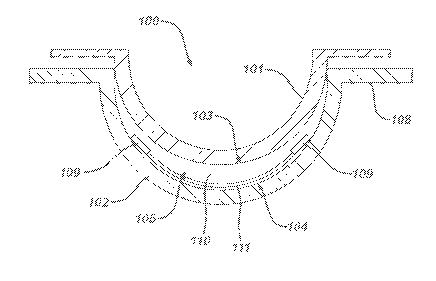
Referring now to Fig. 1, a diagram of an exemplary mold 100 for an
ophthalmic lens is illustrated with a Substrate insert 111. As used herein,
the terms a
mold includes a form 100 having a cavity 105 into which a lens forming mixture
110
can be dispensed such that upon reaction or cure of the lens forming mixture,
an
ophthalmic lens of a desired shape is produced. The molds and mold assemblies
100
8
CA 02862667 2014-07-24
WO 2013/112868
PCT/US2013/023190
are made up of more than one "mold parts" or "mold pieces" 101-102. The mold
parts
101-102 can be brought together such that a cavity 105 is formed between the
mold
parts 101-102 in which a lens can be formed. This combination of mold parts
101-102
is preferably temporary. Upon formation of the lens, the mold parts 101-102
can again
be separated for removal of the lens.
At least one mold part 101-102 has at least a portion of its surface 103-104
in
contact with the lens forming mixture such that upon reaction or cure of the
lens
forming mixture 110 that surface 103-104 provides a desired shape and form to
the
portion of the lens with which it is in contact. The same is true of at least
one other
mold part 101-102.
Thus, for example, a mold assembly 100 may be formed from two parts 101-
102, a female concave piece (front piece) 102 and a male convex piece (back
piece)
101 with a cavity formed between them. The portion of the concave surface 104
which
makes contact with lens forming mixture has the curvature of the front curve
of an
ophthalmic lens to be produced in the mold assembly 100 and is sufficiently
smooth
and formed such that the surface of an ophthalmic lens formed by
polymerization of
the lens forming mixture which is in contact with the concave surface 104 is
optically
acceptable.
The front mold piece 102 can also have an annular flange integral with and
surrounding circular circumferential edge 108 and extends from it in a plane
normal to
the axis and extending from the flange (not shown).
A lens-forming surface can include a surface 103-104 with an optical quality
surface finish, which indicates that it is sufficiently smooth and formed so
that a lens
surface fashioned by the polymerization of a lens forming material in contact
with the
molding surface is optically acceptable. Further, the lens forming surface 103-
104 can
have a geometry that is necessary to impart to the lens surface the desired
optical
characteristics, including without limitation, spherical, aspherical and
cylinder power,
wave front aberration correction, corneal topography correction and the like
as well as
any combinations thereof
At 111, a Substrate insert is illustrated onto which an Energy Source 109 may
be placed. The Substrate insert 111 may be any receiving material onto which
an
Energy Source 109 may be placed, and may also include circuit paths,
components,
and other aspects useful to use of the energy source. The Substrate insert 111
can be a
9
CA 02862667 2014-07-24
WO 2013/112868
PCT/US2013/023190
clear coat of a material which be incorporated into a lens when the lens is
formed. The
clear coat can include for example a pigment as described below, a monomer or
other
biocompatible material. The insert can include a media comprising an insert,
which
can be either rigid or formable. A rigid insert may include an optical zone
providing
An Energy Source 109 may be placed onto Substrate insert 111 prior to
A lens with Substrate insert 111 can include a rigid center soft skirt design
in
which a central rigid optical element is in direct contact with the atmosphere
and the
Substrate insert 111 may be a rigid lens insert fully encapsulated within a
30 The
Substrate insert can be placed in a mold part 101-102 utilized to form an
ophthalmic lens.
CA 02862667 2014-07-24
WO 2013/112868 PCT/US2013/023190
Mold part 101-102 material can include, for example: a polyolefin of one or
more of: polypropylene, polystyrene, polyethylene, poly (methyl methacrylate),
and
modified polyolefin. Other molds can include a ceramic or metallic material.
A preferred alicyclic co-polymer contains two different alicyclic polymers and
is sold by Zeon Chemicals L.P. under the trade name ZEONOR. There are several
different grades of ZEONOR. Various grades may have glass transition
temperatures
ranging from 105 C to 160 C. A specifically preferred material is ZEONOR
1060R.
Other mold materials that may be combined with one or more additives to form
an ophthalmic lens mold include, for example, Zieglar-Natta polypropylene
resins
(sometimes referred to as znPP). An exemplary Zieglar-Natta polypropylene
resin is
available under the name PP 9544 MED. PP 9544 MED is a clarified random
copolymer for clean molding as per FDA regulation 21 CFR (c) 3.2 made
available by
Exxonmobil Chemical Company. PP 9544 MED is a random copolymer (znPP) with
ethylene group (hereinafter 9544 MED). Other exemplary Zieglar-Natta
polypropylene resins include: Atofina Polypropylene 3761 and Atofina
Polypropylene
3620WZ.
Still further, the molds may contain polymers such as polypropylene,
polyethylene, polystyrene, poly (methyl methacrylate), modified polyolefin
containing
an alicyclic moiety in the main chain and cyclic polyolefin. This blend can be
used on
either or both mold halves, where it is preferred that this blend is used on
the back
curve and the front curve consists of the alicyclic co-polymers.
In some methods of making molds 100, injection molding is utilized according
to known techniques. However, molds can be fashioned by other techniques
including,
for example: lathing, diamond turning, or laser cutting.
Stacked Functionalized Layer Inserts
Referring now to Fig. 2, an exemplary design of a Substrate insert 111 which
has been formed as a Stacked Functionalized Layer Insert is illustrated. The
disclosure includes methods to prepare and form the substrate insert that may
be
utilized and formed into Ophthalmic Lenses. For clarity of description, but
not
limiting the scope of the claimed invention, an exemplary Substrate insert 210
is
illustrated and described, which comprises a full annular ring with an optical
lens area
211. It may be obvious to one skilled in the arts that the inventive art
described in this
11
CA 02862667 2014-07-24
WO 2013/112868
PCT/US2013/023190
specification has similar application to the various diversity of shapes that
have been
described generically for Substrate inserts of various kinds.
Referring now to Fig. 3 a three dimensional representation is illustrated of a
fully formed ophthalmic lens using a stacked layer substrate insert of the
type in item
210 is demonstrated as item 300. The representation shows a partial cut out
from the
ophthalmic lens to realize the different layers present inside the device.
Item 320
shows the body material in cross section of the encapsulating layers of the
substrate
insert. This item surrounds the entire periphery of the ophthalmic lens. It
may be clear
to one skilled in the arts that the actual insert may comprise a full annular
ring or other
shapes that still may reside within the constraints of the size of a typical
ophthalmic
lens.
Items 330, 331 and 332 are meant to illustrate three of numerous layers that
may be found in a substrate insert formed as a stack of functional layers. A
single
layer may include one or more of: active and passive components and portions
with
structural, electrical or physical properties conducive to a particular
purpose.
A layer 330 may include an energization source, such as, for example, one or
more of: a battery, a capacitor and a receiver within the layer 330. Item 331
then, in a
non limiting exemplary sense may comprise microcircuitry in a layer that
detects
actuation signals for the ophthalmic lens. A power regulation layer 332 may be
included that is capable of receiving power from external sources, charges the
battery
layer 330 and controls the use of battery power from layer 330 when the lens
is not in a
charging environment. The power regulation may also control signals to an
exemplary
active lens, demonstrated as item 310 in the center annular cutout of the
substrate
insert.
An energized lens with an embedded Substrate insert may include an Energy
Source, such as an electrochemical cell or battery as the storage means for
the energy
and optionally encapsulation, and isolation of the materials comprising the
Energy
Source from an environment into which an ophthalmic lens is placed.
A Substrate insert may also include a pattern of circuitry, components, and
Energy Sources. The Substrate insert may locate the pattern of circuitry,
components
and Energy Sources around a periphery of an optic zone through which a wearer
of a
lens would see. Alternatively, the insert may include a pattern of circuitry,
components and Energy Sources which are small enough to not adversely affect
the
12
CA 02862667 2014-07-24
WO 2013/112868 PCT/US2013/023190
sight of a contact lens wearer and therefore the Substrate insert may locate
them
within, or exterior to, an optical zone.
In general, a Substrate insert 111 may be embodied within an ophthalmic lens
via automation which places an Energy Source a desired location relative to a
mold
part used to fashion the lens.
Fig. 4 illustrates a closer view of a stacked functional layer insert 400 seen
in
cross section. Within the body of the ophthalmic lens 410 is embedded the
functionalized layer insert 420 which may surround and connect to an active
lens
component 450. It may be clear to one skilled in the arts, that this example
shows but
one of numerous embedded functions that may be placed within an ophthalmic
lens.
Within the stacked layer portion of the insert are demonstrated numerous
layers. The layers may comprise multiple semiconductor based layers. For
example,
item 440, the bottom layer in the stack, may be a thinned silicon layer upon
which
circuits have been defined for various functions. Another thinned silicon
layer may be
found in the stack as item 441. In a non-limiting example, such a layer may
have the
function of energization of the device. These silicon layers may be
electrically isolated
from each other through an intervening insulator layer show as item 450. The
portions
of the surface layers of items 440, 450 and 441 that overlap each other may be
adhered
to each other through the use of a thin film of adhesive. It may be obvious to
one
skilled in the arts that numerous adhesives may have the desired
characteristics to
adhere and passivate the thin silicon layers to the insulator, as in an
exemplary sense an
epoxy might.
A multiple stacked layer may include additional layers 442, which in a non
limiting example may include a thinned silicon layer with circuitry capable of
activating and controlling an active lens component. As mentioned before, when
the
stacked layers need to be electrically isolated from each other, stacked
insulator layers
may be included between the electrically active layer and in this example item
451
may represent this insulator layer comprising part of the stacked layer
insert. In some
of the examples described herein, reference has been made to layers formed
from thin
layers of silicon. Material definitions of the thin stacked layers may
include, in a non
limiting sense, other semiconductors, metals or composite layers. And the
function of
the thin layers may include electrical circuitry, but also may include other
functions
like signal reception, energy handling and storage and energy reception to
mention a
13
CA 02862667 2014-07-24
WO 2013/112868 PCT/US2013/023190
few examples. In the case that different material types are used, the choice
of different
adhesives, encapsulants and other materials which interact with the stacked
layers may
be required. For example, a thin layer of epoxy may adhere three silicon
layers shown
as 440, 441 and 442 with two silicon oxide layers 450 and 451.
As mentioned in some of the examples the thinned stacked layer may comprise
circuits formed into silicon layers. There may be numerous manners to
fabricate such
layers, however, standard and state of the art semiconductor processing
equipment may
form electronic circuits on silicon wafers using generic processing steps.
After the
circuits are formed into the appropriate locations on the silicon wafers,
wafer
processing equipment may be used to thin the wafers from hundreds of microns
thick
to thicknesses of 50 microns or less. After thinning the silicon circuits may
be cut or
"diced" from the wafer into the appropriate shapes for the ophthalmic lens or
other
application. In later section, different exemplary shapes of the stacked layer
invention
disclosed herein are shown in Fig. 6. These will be discussed in detail later;
however,
the "dicing" operation may use various technical options to cut out thin
layers with
curved, circular, annular, rectilinear and other more complicated shapes.
When the stacked layers perform a function relating to electrical current
flow,
there may be a need to provide electrical contact between the stacked layers.
In the
general field of semiconductor packaging this electrical connection between
stacked
layers has generic solutions comprising wire bonding, solder bumping and wire
deposition processes. Wire deposition may use a printing process where
electrically
conductive iffl(s are printed between two connection pads. Additionally or
alternatively, wires may be physically defined by an energy source, like for
example a
laser, interacting with a gaseous, liquid or solid chemical intermediate
resulting in an
electrical connection where the energy source irradiates. Still further
interconnection
types may derive from photolithographic processing before or after metal films
are
deposited by various means.
If one or more of the layers needs to communicate electrical signals outside
itself, it may have a metal contact pad that is not covered with passivating
and
insulating layers. These pads may be located on the periphery of the layer
where
subsequent stacked layers do not cover the region. In an example, in Fig. 4
interconnect wires 430 and 431 are demonstrated as electrically connecting
peripheral
regions of layers 440, 441 and 442. It may be apparent to one skilled in the
art that
14
CA 02862667 2014-07-24
WO 2013/112868
PCT/US2013/023190
numerous layouts or designs of where the electrical connection pads are
located and
the manner of electrically connecting various pads together. Furthermore, it
may be
apparent that different circuit designs may derive from the choice of which
electrical
connect pads are connected and to which other pads they are connected. Still
further,
the function of the wire interconnection between pads may be different
including the
functions of electrical signal connection, electrical signal reception from
external
sources, electrical power connection and mechanical stabilization to mention a
few
examples.
In a previous discussion, it was presented that non semiconductor layers may
comprise one or more of the stacked layers in the inventive art. It may be
apparent that
there could be a great diversity of applications which may derive from non-
semiconductor layers. The layers may define energizing sources like batteries.
This
type of layer in some cases may have a semiconductor acting as the supporting
substrate for the chemical layers, or may have metallic or insulating
substrates. Other
layers may derive from layers which are primarily metallic in nature. These
layers
may define antennas, thermal conductive paths, or other functions. There may
be
numerous combinations of semiconducting and non semiconducting layers that
comprise useful application within the spirit of the inventive art herein.
Where electrical connection is made between stacked layers the electrical
connection will need to be sealed after connection is defined. There are
numerous
methods that may be consistent with the art herein. For example, the epoxy or
other
adherent materials used to hold the various stacked layers together could be
reapplied
to the regions with electrical interconnect. Additionally, passivation films
may be
deposited across the entire device to encapsulate the regions that were used
for
interconnection. It may be apparent to one skilled in the art that numerous
encapsulating and sealing schemes may be useful within this art to protect,
strengthen
and seal the stacked layer device and its interconnections and interconnection
regions.
Assembling Stacked Functionalized Layer Inserts
Proceeding to Fig. 5, item 500, a close up view of an exemplary apparatus to
assemble stacked functionalized layer inserts is demonstrated. In the example,
a
stacking technique where the stacked layers do not align on either side of the
layer is
shown. Items 440, 441 and 442 again may be silicon layers. On the right side
of the
CA 02862667 2014-07-24
WO 2013/112868 PCT/US2013/023190
Fig. it may be seen that the right side edge of the items 440, 441 and 442 do
not align
with each other, as they may do. Such a stacking methodology may allow the
insert to
assume a three dimensional shape similar to that of the general profile of an
ophthalmic lens. Such a stacking technique may allow for the layers to be made
from
the largest surface area as possible. In layers that are functional for energy
storage and
circuitry such surface area maximization may be important.
In general many of the features of the previously described stacked inserts
may
be observed in Fig. 5 including stacked functional layers 440, 441 and 442;
stacked
insulating layers 450 and 451; and interconnections 430 and 431. Additionally
a
supporting jig, item 510, may be observed to support the stacked
functionalized layer
insert as it is being assembled. It may be apparent that the surface profile
of item 510
may assume a large number of shapes which will change the three dimensional
shape
of inserts made thereon.
In general, a jig 510 may be provided with a predetermined shape. It may be
coated with different layers, item 520, for a number of purposes. In a non
limiting
exemplary sense, the coating may first comprise a polymer layer that will
allow easy
incorporation of an insert into the base material of an ophthalmic lens, and
may even
be formed from a polysilicone material. An epoxy coating may then be deposited
upon
the polysilicone coating to adhere the bottom thin functional layer 440 to the
coating
520. The bottom surface of a next insulating layer 450 may then be coated with
a
similar epoxy coating and then placed into its appropriate location upon the
jig. It may
be clear that the jig may have the function of aligning the correct placement
of the
stacked layers relative to each other as the device is assembled. In
repetitious fashion,
the rest of the insert may then be assembled, the interconnections defined and
then the
insert encapsulated. The encapsulated insert may then be coated from the top
with a
polysilicone coating. In the case that a polysilicone coating for item 520 is
used, the
assembled insert may be dissociated from the jig 510 by hydration of the
polysilicone
coating.
The jig 510 may be formed from numerous materials. The jig may be formed
and made of similar materials that are used to make molding pieces in the
manufacture
of standard contact lenses. Such a use could support the flexible formation of
various
jig types for different insert shapes and designs. Alternatively, the jig may
be formed
from materials that either in their own right or with special coatings will
not adhere to
16
CA 02862667 2014-07-24
WO 2013/112868 PCT/US2013/023190
the chemical mixtures used to adhere the different layers to each other. It
may be
apparent that numerous options may exist for the configuration of such a jig.
Another aspect of the jig demonstrated as item 510 is the fact that its shape
physically supports the layers upon it. The interconnection between the layers
may be
formed by wirebonding connection. In the process of wirebonding significant
force
may be applied to the wire to ensure it forms a good bond. Structural support
of the
layers during such bonding could be important and could be performed by the
supporting jig 510.
Still another function of the jig demonstrated as item 510 is that the jig may
have alignment features on it that allow for the alignment of pieces of the
functionalized layers to be aligned both relative to each other linearly and
radially
along the surfaces. The jig may allow the alignment of azimutal angle of the
functional layers relative to each other around a center point. Regardless of
the
ultimate shape of the insert produced it may be apparent that the assembly jib
may be
useful in insuring that the pieces of the insert are properly aligned for
their function
and correct interconnection.
Proceeding to Fig. 6, a more generalized discussion of shapes of stacked layer
inserts may be had. In a subset of the generality of shapes consistent with
the art,
some sample variation in shape is shown. For example, item 610 shows a top
view of
a stacked insert which has been formed from essentially circular layer pieces.
The
region shown with cross hatching 611 may be an annular region where layer
material
has been removed. However, it may be apparent that the pieces of the stacked
layers
used form the insert could be disks without an annular region. Although, such
a non
annular insert shape may be of limited utility in an ophthalmic application
the spirit of
the inventive art herein is not intended to be limited by the presence of an
internal
annulus.
Item 620 may demonstrate a stacked functional layer insert. As shown in item
621, the layer pieces may be discrete not only in the stacking direction but
also around
the azimuthal direction perpendicular to the stacking direction. Semicircular
pieces
may be used to form the insert. It may be apparent that in shapes that have an
annular
region, which partial shapes could be useful to reduce the amount of material
that
would need to be "diced" or cut out after the layer material is formed into
its function.
17
CA 02862667 2014-07-24
WO 2013/112868
PCT/US2013/023190
Proceeding further, item 630 demonstrates that non radial, non elliptical and
non circular insert shapes could be defined. As shown in item 630, rectilinear
shapes
may be formed, or as in item 640 other polygonal shapes. In a three
dimensional
perspective pyramids, cones and other geometrical shapes could result from the
different shapes of the individual layer pieces used to form the insert. In
the three
dimensional perspective it may be noted that the individual layers which have
heretofore been represented as planar or flat layer piece themselves may
assume
degrees of freedom in three dimensions. When the silicon layers are thinned
sufficiently they are able to bend or contort around their typical flat planar
shape. This
additional degree of freedom for thin layers allows for even further diversity
of shapes
that may be formed with stacked integrated component devices.
In a more general sense it may be apparent to one skilled in the arts that a
vast
diversity of component shapes may be formed into device shapes and products to
make stacked integrated component devices, and these devices may assume a wide
diversity of functionality, including in a non limiting sense energization,
signal
sensing, data processing, communications both wired and wireless, power
management, electromechanical action, control of external devices and the
broad
diversity of function that layered components may provide.
Powered Layers
Referring now to Fig. 7, item 700, ne or more layers of a functionalized stack
of substrates may include a thin film electrical power source, 706. The thin
electrical
power source may be viewed essentially as a battery on a substrate.
A thin film battery (sometimes referred to as a TFB) may be structured on a
suitable substrate, such as silicon, using known deposition processes to
deposit
materials in thin layers or films. The deposition process for one of these
thin film
layers may include, sputter deposition and may be used to deposit various
materials.
After a film is deposited, it may be processed before a next layer is
deposited. A
common process on a deposited film may include lithography or masking
techniques
that then allow etching or other material removing techniques to be performed
thus
allowing the film layer to have a physical shape in the two dimensions of the
substrate
surface.
18
CA 02862667 2014-07-24
WO 2013/112868 PCT/US2013/023190
In Fig. 7, item 700 an exemplary thin film processing flow may be depicted. A
thin film battery will typically be built upon a substrate, in this flow the
substrate is
depicted in an exemplary sense as an Aluminum Oxide (A1203), item 701. A
typical
layer for electrical contact may next be deposited upon the substrate as shown
in the
Fig. 7 as item 702 where a cathode contact may be formed by a thin film
deposition of
Titanium and Gold upon the substrate. As may be apparent in Fig. 7 this film
may
then be patterned and etched, for example by a sputter etch technique or a wet
etch
technique to yield the shape as shown in item 702. A next step in an exemplary
process would be to form the cathode layer as a film upon the cathode contact,
item
703. One of the commonly utilized cathode films may include Lithium Cobalt
Oxide
(LiCo02) and as shown in Fig.7, it too may have patterning processes performed
upon
it. A next step, as shown as item 704, may be to deposit a thin film to form
an
electrolyte layer in the battery. There may be numerous material choices and
forms for
the electrolyte layer, but in an exemplary sense a polymer layer of Lithium
Phosphorous OxyNitride (LiPON) may be used. Proceeding further to item 705,
the
thin film stack may be further processed with a deposition of Lithium for an
anode
layer and then a copper layer to act as the anode contact layer and like the
other layers
then imaged for an appropriate shape for contact features or other similar
features. The
thin film battery may then be realized by encapsulating the film stack in
passivation
and sealing layers. In exemplary fashion, the layers may be encapsulated with
Parylene and Titanium or with Epoxy and Glass layers as shown in item 706. As
with
other layers there may be patterning and etching of these final layers, for
example to
expose features where the encapsulated battery may be electrically contacted.
It may
be apparent to one skilled in the art, that there are an abundant set of
material choices
for each of the layers.
As described for item 706, enclosure in packaging may be used to prevent
ingress of one or more of: oxygen, moisture, other gasses, and liquids. There
may
therefore be provided packaging in one or more layers which may include one or
more
of an insulating layer, which as a non-limiting may include for example
Parylene,
and an impermeable layer, which may include for example metals, aluminum,
titanium, and similar materials which form an impermeable film layer. An
exemplary
means of forming these layers may include application by deposition onto a
formed
thin film battery device. Other methods of forming these layers may include
applying
19
CA 02862667 2014-07-24
WO 2013/112868 PCT/US2013/023190
organic materials, as for example epoxy, in conjunction with pre-shaped
impermeable
materials. The preshaped impermeable material may include the next layer of
the
integrated component device stack. The impermeable material may include a
precision
formed /cut glass, alumina, or silicon cover layer.
In, for example, a stacked integrated component device for an ophthalmic
device; a substrate may include one that is able to withstand high
temperatures, as for
example 800 deg. C, without chemical change. Some substrates may be formed
from
material which provides electrical insulation and alternatively some
substrates may be
electrically conductive or semi-conductive. These alternative aspects of the
substrate
material, nonetheless, may be consistent with a final thin film battery that
may form a
thin component which may be integrated into a stacked integrated component
device
and provide at least in part the energization function of the device.
In a thin film battery where the thin film battery is a thin component of a
stacked integrated device, the battery may have connection to the other thin
components through access with opening in the passivation films at the contact
pads
shown as items 750 on item 706 of figure 7 item 700. Contact may be made
through
contact pads on the reverse side of the substrate from that shown for items
750.
Contact pads on the reverse side could be electrically connected to the thin
film battery
through the use of a via that is formed through the substrate which has a
conductive
material on the via sidewalls or filling the via. Finally, contact pads may be
formed on
both the top and bottom of the substrate. Some of these contact pads may
intersect
the contact pads of the thin film battery, but alternatives may include
contact pads
through the substrate where no connection is made to the battery. As may be
apparent
to one skilled in the arts, there may be numerous manners to interconnect
through and
to interconnect within a substrate upon which a thin film battery is formed.
The disclosure presented herein may relate to the functions that the
electrical
connections may perform. Some interconnections may provide an electrical
connection path for components within the stack of integrated component
devices and
their interconnection with devices outside the integrated component device
stack. In
relation to connection outside of the device stack; this connection is made
via a direct
electrical conduction path. the connection outside of the package may be made
in a
wireless manner; wherein the connection is made through a manner including
radio
frequency connection, capacitive electrical communication, magnetic coupling,
optical
CA 02862667 2014-07-24
WO 2013/112868
PCT/US2013/023190
coupling, or another of the numerous means that define manners of wireless
communication.
Wire Formed Power Source
Referring now to Fig. 8, an exemplary design of a power source 800 that can
include a battery 810 formed about a conductive wire 820 is depicted. Item 820
may
include a fine gauge copper wire, which may be used as a support. Various
battery
component layers, which schematically are demonstrated as the rings evident in
item
810, may be built up using batch or continuous wire coating processes. In this
manner,
a very high volumetric efficiency, which may reach or exceed 60 % of active
battery
materials, can be achieved in a convenient form factor that is flexible. A
thin wire may
be utilized to form small batteries, such as, in a non-limiting example, a
battery whose
stored energy may include a range measured by milliamp hours. The voltage
capability of such a wire based battery component, may be approximately 1.5
volts. It
may be apparent to a skilled artisan that larger batteries and higher voltages
may also
be scaled, for example by designing the end device to connect single batteries
in
parallel or in series. The numerous manners in which the inventive art may be
used to
create useful battery devices are within the scope of the present invention.
Referring to Fig. 9, item 900, a depiction of how a wire based battery
component may be combined with other components is made. In an example, item
910
may represent an ophthalmic device whose function may be controlled or altered
by
electrical means. When such a device can be part of a contact lens, the
physical
dimensions that components occupy may define a relatively small environment.
Nevertheless, a wire based battery; item 920 may have an ideal form factor for
such an
arrangement, existing on the periphery of such an optical component in a shape
that a
wire may be formed into.
Referring now to Fig. 10, item 1000, the result of processing using an
exemplary method for forming wire batteries is illustrated. These methods and
the
resulting products define a wire based battery. Initially, a copper wire, item
1010, of
high purity such as those available from a commercial source, for example
McMaster
Carr Corp. may be chosen and then coated with one or more layers. It may be
apparent
that there exist numerous alternatives of the type and composition of the wire
that may
be used to form wire based batteries.
21
CA 02862667 2014-07-24
WO 2013/112868 PCT/US2013/023190
A zinc anode coating may be used to define an anode for the wire battery as
shown as item 1020. The anode coating may be formulated from zinc metal
powder,
polymer binders, solvents, and/or additives. The coating may be applied and
immediately dried. Multiple passes of the same coating may be used to achieve
a
desired thickness.
Continuing with Fig. 10, the anode and cathode of the wire battery may be
separated from each other. A separator coating, item 1030, may be formulated
from
non-conductive filler particles, polymer binders, solvents, and additives. The
method
of application of the separator may be a coating application method similar to
that used
to coat the anode layer 1020.
A next step in processing the exemplary wire battery of item 1000 is forming a
cathode layer. This cathode, item 1040 may be formed with silver oxide cathode
coating. This silver oxide coating may be formulated from Ag20 powder,
graphite,
polymer binders, solvents, and additives. In similar fashion to the separator
layer, a
common coating application method may be used as was used for other layers of
the
wire battery.
After a collector is formed, the exemplary wire battery may be coated with a
layer to collect current from the cathode layer. This layer may be a
conductive layer
from a carbon impregnated adhesive. Alternatively, this layer may be a metal,
for
example Silver, impregnated adhesive. It may be apparent to one skilled in the
art that
there are numerous materials that may support forming a layer to enhance the
collection of current along the battery surface. Electrolyte (as for example,
potassium
hydroxide solution with additives) may be applied to the assembled battery to
complete
construction.
In a wire battery, the layers that are used to form the battery may have an
ability to evolve gasses. The materials that form the battery layers may have
a sealant
layer placed around the battery layers to contain the electrolyte and other
materials
within the confines of the battery and to protect the battery from mechanical
stresses.
Nevertheless, this sealant layer is typically formed in a manner that allows
the
diffusion of the evolved gasses through the layer. Such a sealant layer may
include
silicone or fluoropolymer coatings; however, any material which is used in the
state of
the art to encapsulate batteries of this type may be used.
22
CA 02862667 2014-07-24
WO 2013/112868 PCT/US2013/023190
Components of Stacked Multilayer Interconnection
As mentioned in prior description, the layers of a stacked integrated
component
device may typically have electrical and mechanical interconnections between
them.
A description has been given of certain interconnection schemes in which for
example
wire bonds are included in sections preceding this discussion. Nevertheless,
it may be
helpful to summarize some of the types of interconnection in their own right
to help in
explanation of the art.
One of the common types of interconnection derives from the use of a "solder
ball." A solder ball interconnection is a type of packaging interconnection
that has
been used for decades in the semiconductor industry, typically in so-called
"flip chip"
applications where chips are connected to their packaging by inverting a diced
electronic "chip," that has deposited solder balls on its interconnections,
onto a
package that has aligned connection pads to connect to the other side of the
solder ball.
Heat treatment may allow the solder ball to flow to a certain degree and form
an
interconnection. The state of the art has continued its progress so that the
solder ball
type of interconnection may define an interconnection scheme that occurs on
either or
both sides of a layer. Additional improvement has occurred to decrease the
dimension
of solder balls that may reliably be used to form interconnections. The size
of the
solder ball may be 50 microns in diameter or smaller.
When a solder ball interconnection is used between two layers, or more
generally when an interconnection scheme is used that creates gaps between two
layers, a process step of "underfill" may be used to place adhesive material
into the
gaps to provide adhesive mechanical connection and mechanical support of the
two
layers. There are numerous manners to underfill a set of layers that have been
interconnected. In some manners the underfill adhesive is pulled into the gap
area by
capillary action. The underfill adhesive may be made to flow into a gap by
pressurizing the liquid into the gap region. An evacuated state in the gap
area may be
formed by pulling a vacuum upon the layered device and then following this
with
application of the underfill material. Any of the numerous manners to
underfill a gap
in two layered materials are consistent with the art herein described.
Another evolving technology of interconnection relates to interconnection of
one side of a layered component to the other side by a via that cuts through
the layer ¨
such a feature is typically called a through via. The technology has also been
around
23
CA 02862667 2014-07-24
WO 2013/112868 PCT/US2013/023190
for decades in various forms; however the state of the art has improved where
very
small vias in the 10 micron or less diameter dimension are possible with
extremely
large aspect ratios possible as well, especially when the layered material is
formed of
Silicon. Regardless of the layer material, a through via may form an
electrical
interconnection between the two surfaces of a layer with a metallic; however,
when the
layer is a conductive or semiconductive material, the through via must have an
insulator layer insulating the metallic interconnection from the layer itself.
The
through via may penetrate through the entire layered substrate. Alternatively,
the
through via may penetrate the substrate but then intersect with a deposited
feature on
the surface of the substrate; from the back side.
In through vias where the via intersects with a metal pad on one side of the
layer, that metal pad may be interconnected to a different layer with numerous
manners
including solder balls and wire bonds. In the case that the via can be filled
with metal
and penetrates the entire layered substrate it may be useful for
interconnections to be
formed by solder balls on both sides of the interconnecting via.
Another interconnection occurs when a layer is formed which only has through
vias and metal routing line upon it. In some cases, such an interconnection
device may
be called an interposer. Since the interposer layer may only have metal
routings and
via interconnections there are some additional materials that the layer may be
made of
and therefore alternatives for how to create through vias in these materials.
As a non-
limiting example, a silicon dioxide or quartz substrate may be the material of
the layer.
In some cases this quartz layer may be formed by pouring melted quartz upon a
substrate where metallic filaments protrude from the surface. These
protrusions then
form the metallic connections between the top and bottom surface of the quartz
layer
that results from this type of processing. The numerous manners of forming
thin
interconnecting layers comprise art useful in interconnecting stacked layers
and
therefore in the forming of stacked integrated component devices.
Another type of interconnection element is derived from the through substrate
via art. If a through substrate via is filled with various layers including
metal layers
the resulting via may form a structure that can be cut. The via may be cut or
"diced"
down its center forming a cut out half via. Interconnections of this type may
be termed
castellation interconnections. Such interconnections provide connection from a
top
surface to a bottom surface and the ability of interconnections from these
surfaces; but
24
CA 02862667 2014-07-24
WO 2013/112868 PCT/US2013/023190
as well the potential for interconnection from the side may derive from the
structure of
the "Castellation."
A number of interconnection and component integration technologies have
been discussed herein. Nevertheless, the invention disclosed herein is
intended to
embrace a wide diversity of integration technologies and the examples, which
are
intended for illustration purposes, are not intended to limit the scope of the
art.
Stacked Integrated Component Device with Energization
Proceeding to Figure 11, an exemplary stacked integrated component device is
portrayed as item 1100. As can be seen, item 1100 may be comprised by 8
individual
layers that are identified as items 1101-1108 in the figure. These layers will
be
described in more detail, but it is clear that additional or fewer layers may
be possible
within the scope of the invention.
The stacked integrated component device of item 1100 may have a substrate base
as shown in item 1108. Such a substrate base may provide a function of
mechanical
support for the device. Such a layer may provide both a mechanical support
function
and an encapsulation function, as other layers, for example 1107, of the
device are
connected and sealed upon the substrate, 1108. Item 1100 has numerous
interconnections depicted between the layers and items 1130 and 1131
identifies an
example rendering of such an interconnection. Although the numerous manners of
interconnection may provide this function, it may be helpful to view these
interconnections as solder balls in an exemplary manner. Items 1130 and 1131
may be
an electrical connection between items 1108 and 1107 or they may function for
a
mechanical interconnection between the layers. Additionally, the space between
items
1130 and 1131 is identified as item 1140. This item is intended to represent
the fact
that the space in between layers may be underfilled with an adhesive to
provide
mechanical connection and layer support.
The substrate layer, 1108, may have electrically active functions. This may
derive
from the substrate having electrical circuitry upon it, as may be the case if
the substrate
was a semiconductor substrate with integrated electronic circuitry on it.
Alternatively,
electrical function may derive from the substrate having deposited layers of
conductive
material to perform functions such as defining antennas or passive electrical
devices as
CA 02862667 2014-07-24
WO 2013/112868 PCT/US2013/023190
for example capacitors and resistors. Still further electrical active function
may derive
if the substrate is a metallic layer where the entire layer could provide an
electrical
ground connection or an electrical shielding for the stacked integrated
device.
The substrate layer, 1108, may also provide a function of providing thermal
communication of the stacked integrated device to its environment. The layer
may be
formed of a highly thermally conductive metallic substrate capable of allowing
high
flows of thermal energy to flow across it. Alternatively, the substrate may
act to
insulate the device stack from the environment below it. There may also reside
within
the substrate layer the ability to sense the environment below the stacked
integrated
device both for thermal and non-thermal characteristics. There may be numerous
functions that the bottom layer of a stacked integrated component device may
perform.
Proceeding to an exemplary layer, item 1103, in the middle of the stacked
integrated component device, item 1100, an interconnection layer may be
present.
Such a layer may have numerous electrical connection locations upon it. This
layer
may serve the function of an electrical "Bus" or routing device allowing
signals from
various components to be interconnected. Electrical devices from layers either
above
or below the interconnection device may be connected to each other.
Alternatively,
signals may flow through the body of the interconnect layer and route between
the
layers above and below the interconnect device as schematically indicated by
the
"solder ball" features shown above and below layer 1103. Such an
interconnection
layer may be a layer comprised of a mechanical substrate with vias and
metallic
routing lines where control of these routing lines is performed by circuitry
above or
below the interconnect plane. However, alternatives may exist where the layer
1103
also has active electrical functions to act for controlling signal and power
routing or for
effecting electrical signals, as may be the function of passive devices like
resistors,
capacitors and inductors for example. In a similar fashion, item 1105, may
provide
routing and mechanical support as an interconnect layer connecting electrical
devices
from one layer, for example 1104, with other types of electrical devices such
as a
battery layer that may be illustrated as layer 1106. Interconnect layer, item
1110, may
define an interconnect device that occupies only a portion of the space
available in a
layer, for example item 1102. It may be apparent that numerous interconnect
layers
and types of interconnect layers may comprise an important function in stacked
integrated devices.
26
CA 02862667 2014-07-24
WO 2013/112868 PCT/US2013/023190
Passive devices may be added to the stacked integrated component device as a
layer or portion of a layer discrete from the technology layers. In these
devices, as for
example item 1120, one or more passive devices may be incorporated into a
layer
device in its own right. This passive layer device may be formed in an
integrated
processing fashion where the devices are processed into the substrate
material.
Alternatively, the layer may be formed from discrete passive components
assembled
onto an appropriate layer form. In some cases, the performance of the passive
devices
may be superior when processed in this manner to a similar passive device
formed as
part of the integrated CMOS or other technology layers. Another motivation may
be a
lowered cost structure. Numerous types of passive devices may be consistent
with the
art herein including in a non-limiting exemplary sense, resistors, capacitors,
diodes,
fuses, inductors, transformers, antennas, and suppressors.
The integrated passive device layer may incorporate the diversity of the
interconnection purposes that an interconnect device layer may perform. As
indicated
in figure 11, item 1100 the integrated passive device, item 1120 may connect
to other
layers through solder ball connections. As well, the device may include
through
substrate connection elements that allow the device to connect to both layers
above and
below it, or to pass signals through it. As may be apparent to one skilled in
the arts,
the integrated passive device function may be performed in a dedicated layer
location
as shown in item 1100; however, as well, there may be a number of such devices
incorporated and be within the intent of the inventive art herein.
An important function in some stacked integrated component devices may be
performed by the integrated circuit s incorporated into the device.
Schematically, these
devices are represented by the technology layers identified as items 1102 and
1104.
Where there may be multiple technology layers, the stacked integrated
component
device may have technology that differs in the separate layers. In an
exemplary sense,
the technology of layer 1 item 1102 may derive from a CMOS technology
processing
flow; while the technology of layer 2, item 1104 may derive from a BiCMOS
technology processing flow. It may be apparent to one skilled in the arts that
numerous technology combinations may be possible including mentioning a few
examples, CMOS, BiCMOS, Bipolar, MEMS, Memory Device and other technology
consistent with producing a function on a substrate consistent with layer
formation.
27
CA 02862667 2014-07-24
WO 2013/112868 PCT/US2013/023190
The technology type of items 1102 and 1104 may be similar but come from a
different family within that technology definition. For example, Item 1102 may
be
formed in a 0.5 micron CMOS processing flow; whereas Item 1104 may be formed
in
a 20 nanometer CMOS processing flow in a non-limiting exemplary sense. An
exemplary motivation for splitting device function into two separate
technology blocks
may include the cost effectiveness of the resulting multicomponent device. The
motivation may include technology improvements that a particular technology
node
would offer the device; including for example that the power draw of some
critical
function may be dramatically lowered by its design being in an advanced narrow
linewidth technology. The two layers may be from the same technology node and
the
same technology type but represent different circuit designs within those
technology
and technology node. The substrates used to form the technology layer itself
may
differ; as for example would be the case if technology layer 1, item 1102 were
formed
upon a standard silicon substrate and technology layer 2 were formed upon a
substrate
that derives from a different substrate including in a non-limiting sense a
silicon on
insulator substrate, or a non-Silicon semiconductor substrate, or an organic
electronic
device substrate as some examples. In a more general sense, it may be clear to
one
skilled in the arts that a very wide combination of technology types, designs
and nodes
may be combined into embodiments of one or more technology layers and include
art
consistent with the invention herein.
The technology layer may be formed from a standard thinned substrate layer
produced in a particular technology family, where interconnection to the
device layer
may occur through one side of the layer as is depicted in device 1102.
Alternatively,
the technology layer may include through layer interconnection to allow both
sides of
the layer to interconnect with layers above and below itself, as depicted in
item 1104.
It may be obvious to one skilled in the art, that the similar diversity of
interconnection
schemes as has been previously described may be consistent with the inventive
art
herein.
In the discussions of the stacked integrated component devices herein, the
descriptions and drawings of layers may derive from planar layers that are
assembled
into the various forms and shapes that have been described including those
examples
shown in figure 6. It may be important to note however that the thin layers
may also
be formed into non-planar layer shapes as well. There may be numerous manners
to
28
CA 02862667 2014-07-24
WO 2013/112868 PCT/US2013/023190
form such non planar shapes ranging from deformation of the thin layer
structures into
a three dimensional shape to dicing the layers in such a way that non planar
shapes
may be formed by deforming the thin layered shape. Therefore, the scope of the
description is meant to embrace the diversity of three dimensional form
factors that a
layered device formed from stacked integrated component devices may define.
Proceeding to the top layer of item 1100, as shown as item 1101, this layer
may
have similar additional functions due to its geometry of being on top of the
other layers
that the substrate layer 1108 has by being on the bottom of the layer stack.
Therefore,
it may have similar embodiments to those discussed for layer 1108. In the
example of
item 1100, the top layer may function to provide wireless communication of
signals
and power in and out of the stacked integrated component device through use,
for
example of a coiled antenna feature. Item 1101 is depicted as having wired
connections only to the layer below itself Nevertheless, it may alternatively
be
possible for interconnections external to the device to occur on this layer as
well. It
may be apparent that the top layer may actually perform any of the layer type
functions
that have been described herein.
Proceeding to Fig. 12, item 1200 similar to item 1100 is demonstrated. A
Stacked
Integrated Component Device with energization is shown where there are 8
stacked
layers present. There is a top layer 1210, which asks as a wireless
communication
layer. There is a technology layer 1215, which connects to the top layer 1210
and to
an interconnect layer 1225 below it. Furthermore, there are 4 battery layers
depicted as
item 1230. There may be a lower substrate layer, item 1235 where the substrate
includes an additional antenna layer. There may be numerous functions that
could be
performed; however, in a non-limiting exemplary sense one function could be
the
function of an RF Signal repeater.
In the exemplary function as an RF Signal repeater, item 1210 may function as
follows. The stacked integrated component device has energization
capabilities. The
stored energy resides in the battery layers of item 1230. There may be
numerous ways
to configure the battery elements of layer 1230; however, an example would be
where
a stack of four elements would be connected in a parallel configuration to
yield an
operating voltage in a 3.6V regime. The four stacks of four elements could
likewise be
connected in a parallel configuration where the energy output from each stack
is fed
through the interconnect layer 1225 to the Power Management device, 1220, in
the
29
CA 02862667 2014-07-24
WO 2013/112868 PCT/US2013/023190
technology layer 1215. The power management device 1220 may have a sense
function that will determine whether all of the battery chains are fully
functional and
isolate any low charged or non-functional battery chains from the others.
Device 1220
may also take the input voltage of 3.6 V and provide a Power Supply function,
1240,
by altering the operating voltage to a 2.5 Volt supply which it would output
to the
power supply connections and distribution network of item 1225, the
interconnect
layer. This supply voltage may power the RF Transceiver, 1245, the Control
Function
Device, 1250 and provide the power supply connections to the integrated
passive
device item 1255. The power supply may charge capacitors located in the
integrated
passive device, 1255. These capacitors may serve the function of buffering
power
demands as the other technology devices draw power. Although specific details
have
been discussed, it may be clear that significant variation may be possible
with the type
of design represented by item 1200.
When the energy supply system is fully charged and the power management unit
is
providing appropriate output power, device 1200 may function as a signal
repeater as
follows. The coil Antenna of item 1210 may be designed to be tuned to a
frequency;
which may be 2.44GHz for example. Additional filtering stages may be found for
a
passive device based RF filter also tuned to 2.44 GHz. Signals detected at
this
frequency may be shuttled along the interconnect device 1225 to the RF
transceiver,
1245 of the technology layer 1215. The RF Transceiver, 1245, may as well be
tuned
to a spectrum of frequencies around 2.44 GHz. When the transceiver, 1245
detects
signals on in this spectral range it may then provide an amplification
function on the
signals and then retransmit them as well as sending a control signal to the
control
function device 1250. When the control function, 1250, receives the
appropriate
control information from device 1245 it may then route the output of the RF
Transceiver 1245, through the interconnect layer 1225, along through vias in
the
battery elements of item 1230 to the antenna of level 1235 for retransmission.
At the
same time that the RF Signal repeater function is being performed in the
exemplary
device 1200, another parallel function of battery recharging may be occurring.
In a
similar manner to the previous discussion, there may be an antenna in the top
layer
1210 tuned to a different higher frequency of 15.5MHz for example. When this
signal
is routed through the Integrated Passive device, 1255, it may be sent through
to the
interconnect layer 1225 and then on to the Power Management device 1220. The
CA 02862667 2014-07-24
WO 2013/112868 PCT/US2013/023190
Power Management device may take the power from this signal and then convert
the
signal from an AC signal to a DC Charging signal. It may then switch one of
the
battery units of layer 1230 from providing power to being charged. In this
manner the
stacked integrated component device, 1200, may be performing a function and
may be
reenergized at the same time. Item 1210 is one of many examples that may
derive
from the inventive art discussed herein; its description is focused on
describing how
some exemplary parts of a stacked integrated component device may function.
Proceeding now to figure 13, item 1300 will be described. As may be observed
in
the figure, the layers of item 1300 may exhibit similarity to the previously
discussed
item 1200. And, as an example a similar type of functioning of the device
layer as
described for item 1200 may be operant in item 1300. However, There may be a
lessened number of layers, the antennal layer 1210 on top of the stacked
integrated
component device, a technology layer 1215 with similar devices as item 1200,
and an
interconnect substrate layer item 1225. An important difference of item 1300
may
come from the external connection of both energization components and other
external
components as shown by item 1320. Recalling the wire battery component of item
920; the energy storage for the stacked integrated component device 1300 may
exist as
the element of item 1320. It may be connected via a wire bond connection to
the
interconnect layer 1225. An additional function of such a wire battery may be
for the
wire to function as an antenna device as well. Therefore, the transmission
signal
produced by the technology layer 1215 may be routed to the battery wire as
well. An
external power device and the externally connected components may be defined
by a
wire battery 1320. However it may be apparent to one skilled in the art that
multiple
separate devices may be externally connected within the scope of this art; and
furthermore, that a variety of battery type devices including, without
limitation, flat
planar batteries of the type described as the output of processing flow 700
may be
utilized and also be within the scope of the art contained herein.
31
CA 02862667 2014-07-24
WO 2013/112868 PCT/US2013/023190
Ophthalmic Lenses May Incorporate Stacked Integrated Component Device with
Energization
Amongst the significant diversity of applications and functions that a stacked
integrated component device with energization might perform, an interesting
subset
may relate to the incorporation of the stacked integrated component device
into an
ophthalmic lens. Without limiting the generality of embodiments that the
inventive art
herein may define, it may be illustrative to consider how the various elements
that have
been discussed could bear relevance to ophthalmic devices.
In an example of an ophthalmic device containing stacked integrated devices
with
energization an ophthalmic lens may contain an electroactive lens component
which
responds to electrical signals to change the optical power of the lens, and
when worn in
an ophthalmic lens, then the optical power into the eyes of a user may be
usefully
controlled. Such an ophthalmic application may define a very limited space for
the
inclusion of devices and therefore, may be improved by the incorporation of
thin
stacked devices to provide function. Additionally, the shape of an ophthalmic
lens is
three dimensional object more similar to the surface of a sphere than to a
flat plane;
therefore, placing stacked devices whose shapes conform to circular shapes may
allow
for the optimization of utilized space. It may be important to understand,
that a small
stacked device which is planar and rectilinear may also comprise art
consistent with an
ophthalmic lens application. The stacked devices may in their variety of
shapes be
included into an insert which encapsulates the stacked devices and provides
material
aspects that are consistent with the materials that were described herein in
the
manufacture of ophthalmic lenses.
Continuing with the exemplary ophthalmic device, a stack of energized
components may provide a number of functions which may be important in an
ophthalmic lens application including the reception of external control
signals and the
activation of components based on the control signal. In addition, it may be
useful in
some applications to reenergize the battery device and the types of function
towards
charging that have been discussed may be useful. Alternatively, a wire battery
as an
external component may provide a battery that functions for a single discharge
cycle.
The energized components that receive control signals via wireless input may
then
enact a controller to set a particular voltage output. The output may then be
routed via
an external connection to the electroactive lens and change the optical power
of the
32
CA 02862667 2014-07-24
WO 2013/112868 PCT/US2013/023190
ophthalmic lens. In these manners, the utility of the various aspects of the
inventive art
described herein may be appreciated.
33