Note: Descriptions are shown in the official language in which they were submitted.
81781502
NOISE SHIELDING TECHNIQUES FOR ULTRA LOW CURRENT
MEASUREMENTS IN BIOCHEMICAL APPLICATIONS
BACKGROUND OF THE INVENTION
[0001] Advances in micro-miniaturization within the semiconductor
industry in recent
years have enabled biotechnologists to pack traditionally bulky sensing tools
into smaller and
smaller form factors, onto so-called biochips. As device dimensions shrink, it
would be
desirable to develop high sensitivity measurement techniques for biochips.
SUMMARY OF THE INVENTION
[0001a] According to one aspect of the present invention, there is
provided a device
having an integrated noise shield, comprising: a plurality of vertical
shielding structures
substantially surrounding a semiconductor device, wherein the vertical
shielding structures
comprise a plurality of vias, and wherein the plurality of vias are arranged
in a plurality of
concentric squares or rings, and wherein the vias in a first concentric square
or ring of vias are
offset from the vias in a second concentric square or ring of vias; and an
opening above the
semiconductor device, the opening is configured to allow a conductive fluid to
be introduced
such that the opening is substantially filled with the conductive fluid;
wherein the plurality of
vertical shielding structures and the conductive fluid shield the
semiconductor device from
ambient radiation.
[0001b] According to another aspect of the present invention, there is
provided a
method for shielding a device from noise, comprising: providing a plurality of
vertical
shielding structures substantially surrounding a semiconductor device, wherein
the vertical
shielding structures comprise a plurality of vias, and wherein the plurality
of vias are arranged
in a plurality of concentric squares or rings, and wherein the vias in a first
concentric square
or ring of vias are offset from the vias in a second concentric square or ring
of vias; and
providing an opening above the semiconductor device, wherein the opening is
configured to
allow a conductive fluid to be introduced such that the opening is
substantially filled with the
conductive fluid; wherein the plurality of vertical shielding structures and
the conductive fluid
shield the semiconductor device from ambient radiation.
1
CA 2863318 2018-10-11
81781502
BRIEF DESCRIPTION OF THE DRAWINGS
[0002] Various embodiments of the invention are disclosed in the
following detailed
description and the accompanying drawings.
[0003] Figure 1 is a block diagram illustrating an embodiment of a
sensor circuit 100
.. for measuring a physical property, such as a current, voltage, or charge,
within a single cell of
a bio-sensor array using an integrating amplifier.
[0004] Figure 2 is a diagram illustrating a cross-sectional view of an
embodiment of a
semiconductor device 200 with an integrated noise shield.
[0005] Figure 3A is a diagram illustrating a top-view of an exemplary
configuration of
vertical shielding structures 218.
100061 Figure 3B is a second diagram illustrating a top-view of
another exemplary
configuration of vertical shielding structures 218.
[0007] Figure 4 is a diagram illustrating a cross-sectional view of an
embodiment of a
semiconductor device 400 with an integrated noise shield.
DETAILED DESCRIPTION
[0008] The invention can be implemented in numerous ways, including as
a process;
an apparatus; a system; a composition of matter; a computer program product
embodied on a
computer readable storage medium; and/or a processor, such as a processor
configured to
execute instructions stored on and/or provided by a memory coupled to the
processor. In this
specification, these
la
CA 2863318 2018-10-11
CA 02863318 2014-07-29
WO 2013/122672 PCT/US2012/069911
implementations, or any other form that the invention may take, may be
referred to as techniques.
In general, the order of the steps of disclosed processes may be altered
within the scope of the
invention. Unless stated otherwise, a component such as a processor or a
memory described as
being configured to perform a task may be implemented as a general component
that is temporarily
configured to perform the task at a given time or a specific component that is
manufactured to
perform the task. As used herein, the term 'processor' refers to one or more
devices, circuits,
and/or processing cores configured to process data, such as computer program
instructions.
[0009] A detailed description of one or more embodiments of the invention
is provided
below along with accompanying figures that illustrate the principles of the
invention. The
invention is described in connection with such embodiments, but the invention
is not limited to any
embodiment. The scope of the invention is limited only by the claims and the
invention
encompasses numerous alternatives, modifications and equivalents. Numerous
specific details are
set forth in the following description in order to provide a thorough
understanding of the invention.
These details are provided for the purpose of example and the invention may be
practiced according
to the claims without some or all of these specific details. For the purpose
of clarity, technical
material that is known in the technical fields related to the invention has
not been described in
detail so that the invention is not unnecessarily obscured.
[0010] Nanopore membrane devices having pore sizes on the order of 1
nanometer in
internal diameter have shown promise in rapid nucleotide sequencing. A
nanopore is a very small
hole, and the nanopore can be created by a pore-forming protein or as a hole
in synthetic materials,
such as silicon or graphene. When a voltage potential is applied across the
nanopore immersed in a
conducting fluid, a small ionic current arising from the conduction of ions
across the nanopore can
be observed. When a molecule, such as a DNA or RNA molecule, passes through
the nanopore,
the molecule can partially or completely block the nanopore. Since the size of
the ionic current is
sensitive to the pore size, the blockage of the nanopore by the DNA or RNA
molecule causes a
change in the magnitude of the current through the nanopore. It has been shown
that the ionic
current blockage can be correlated with the base pair sequence of the DNA
molecule.
[0011] However, molecule characterization using nanopore membrane devices
face various
challenges. One of the challenges is measuring very low-level signals: the
magnitude of the ionic
current through the nanopore is very low, typically on the order of a few tens
or hundreds of
picoamps (pA). Therefore, detecting any changes in such a low-level current
through the nanopore
becomes very challenging.
2
CA 02863318 2014-07-29
WO 2013/122672 PCT/US2012/069911
[0012] One effective circuit technique for measuring low-level current is
using an
integrating amplifier. Using an integrating amplifier to measure low-level
current has several
advantages. The integrating amplifier averages the current over many
measurement periods, which
helps mitigate the effects of noise to some degree. The integrating amplifier
also limits the
bandwidth to the bandwidth of interest without the need for additional
filtering. The circuitry for
the integrating amplifier at the measurement site is also small as compared to
those corresponding
to other measurement techniques, thus making it feasible to fabricate a bio-
sensor array with a large
array of measurement cells, which is highly desirable for identifying
molecules in applications such
as single strand DNA characterization.
[0013] Figure 1 is a block diagram illustrating an embodiment of a sensor
circuit 100 for
measuring a physical property, such as a current, voltage, or charge, within a
single cell of a bio-
sensor array using an integrating amplifier. As shown in Figure 1, a physical
property is detected
by detector 102 as detected signal 104. Sensor circuit 100 may be used to
measure the mean value
of detected signal 104 without sampling, as described further below.
[0014] In some embodiments, an initiation flag 106 resets an integrating
amplifier 108 and
starts a continuous integration of detected signal 104 over time. Integrated
output 110 is compared
with a trip threshold 114 using a comparator 112. When integrated output 110
reaches trip
threshold 114, a trip flag 116 may be used as a feedback signal to integrating
amplifier 108 for
terminating the integration of detected signal 104. For example, when trip
flag 116 is "on" or
asserted, the integration is terminated. The duration of time between the
assertion of initiation flag
106 and the assertion of trip flag 116 is proportional to the mean value of
detected signal 104, e.g.,
the mean value of a current. Accordingly, the "on" and "off" of trip flag 116
(only 1 bit of
information) may be sent from the cell to an external processor for
calculating the mean value of
detected signal 104. Alternatively, the "on/off" information may be sent from
the cell to an
external storage for delayed processing. For example, the clock cycles at
which initiation flag 106
and trip flag 116 are respectively asserted may be recorded in an external
storage. The number of
clock cycles between the two asserted flags may then be used to determine the
mean value of
detected signal 104 at a later time.
[0015] In some embodiments, more accurate results may be obtained by
integrating
detected signal 104 over multiple integrating cycles. For example, the
determined mean value of
detected signal 104 may be further averaged over multiple integrating cycles.
In some
embodiments, initiation flag 106 is based at least in part on trip flag 116.
For example, initiation
flag 106 may be re-asserted in response to trip flag 116 being asserted. In
this example, trip flag
3
CA 02863318 2014-07-29
WO 2013/122672 PCT/US2012/069911
116 is used as a feedback signal for reinitializing integrating amplifier 108,
such that another cycle
of integration of detected signal 104 may begin as soon as the previous cycle
of integration is
terminated. Re-asserting initiation flag 106 immediately after trip flag 116
is asserted reduces the
portion of time when detector 102 generates a signal that is not integrated
and thus not measured.
The integration occurs over approximately the entire time that the signal is
available. As a result,
most of the information of the signal is captured, thereby minimizing the time
to obtain an average
value for the measured signal.
[0016] The sensitivity of sensor circuit 100 is maximized by continuously
integrating
detected signal 102 without sampling. This serves to limit the bandwidth of
the measured signal.
With continuous reference to Figure 1, trip threshold 114 and an integration
coefficient A set the
bandwidth of the measured signal. As integration coefficient A decreases or as
trip threshold 114
increases, the measured signal bandwidth decreases.
[0017] However, the low-current measuring circuit is susceptible to
different noise sources,
including external noise sources and noise sources within the measuring
circuit itself. External
noise sources affecting the performance of the low-current measuring circuit
are numerous,
including alternating current (AC) line noise, ballast noise from florescent
light fixtures,
electromagnetic interference (EMI), and the like.
[0018] Internal noise sources affecting the performance of the low-current
measuring circuit
include voltage and noise components from the integrating amplifier, as well
as resistive noise from
the measurement source. These components are amplified by the noise gain of
the integrator,
which is equal to (1 + Cin/Cfb), where Cin is the total input capacitance, and
Cfb is the integration
capacitor (i.e., the feedback capacitor (Cfb ) for the integrating amplifier).
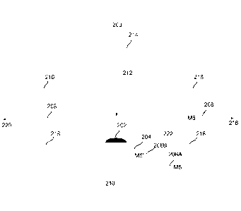
[0019] Figure 2 is a diagram illustrating a cross-sectional view of an
embodiment of a
semiconductor device 200 with an integrated noise shield. In some embodiments,
semiconductor
device 200 is a nanopore device in a single cell of a nanopore array, and the
integrated noise shield
shields the nanopore device from both external noise sources and internal
noise sources. In some
embodiments, the integrated noise shield disclosed herein can also be
integrated into other types of
bio-sensor semiconductor arrays, such as bio-sensor semiconductor arrays in
which low-level
signal measurements susceptible to different noise sources are made. A
nanopore device is used
hereinafter as an example for semiconductor device 200. However, a nanopore
device is selected
for illustration purposes only; accordingly, the present application is not
limited to this specific
example only.
4
CA 02863318 2014-07-29
WO 2013/122672 PCT/US2012/069911
[0020] The integrated noise shield surrounds and shields the portions of
semiconductor
device 200 that are susceptible to different noise sources. For example, with
continued reference to
Figure 2, the portions of semiconductor device 200 that are susceptible to
noise include a biological
sample 202, a measurement electrode 204, other measurement integrated
circuitries (not shown in
the figure), and the like, and these portions of semiconductor device 200 are
surrounded and
shielded by the integrated noise shield. The integrated noise shield can be
formed using any
conductive material.
[0021] The integrated noise shield includes a bottom shield. With continued
reference to
Figure 2, the bottom shield includes one or more conductive layers (206A and
206B) that are
placed below the portions of semiconductor device 200 that arc susceptible to
noise. In some
embodiments, conductive layer 206A is metal layer 5 (M5), which is the metal
layer below the top
metal layer 208 (M6) of semiconductor device 200. Conductive layer 206B is
metal layer 5' (1\45'
or MTM Cap layer), which is a metal layer sitting on top of M5 with a thin
layer of oxide 210 in
between. In some embodiments, the bottom shield is formed using conductive
materials other than
metal, including polycrystalline silicon, and the like. In some embodiments,
semiconductor device
200 includes other conductive layers, such as a layer of substrate. Since the
layer of substrate is
typically thick and conductive, it acts as a bottom shield layer for
semiconductor device 200.
[0022] The integrated noise shield includes a top shield. The top shield
includes a
conductive layer 208 with an opening 212. With continued reference to Figure
2, the conductive
layer 208 of the top shield is a metal layer placed above the portions of
semiconductor device 200
that are susceptible to noise. In some embodiments, conductive layer 208 is
metal layer 6 (M6),
which is the top metal layer of semiconductor device 200. In some embodiments,
opening 212
allows biological sample 202 to be introduced into semiconductor device 200
such that biological
sample 202 can be tested or analyzed by semiconductor device 200.
[0023] The top shield further includes a conductive liquid shield 214
deposited over and
covering the portions of semiconductor device 200 that are susceptible to
noise, including
biological sample 202. Without conductive liquid shield 214, opening 212 would
expose
semiconductor device 200 to different noise sources. In addition, conductive
layer 208 (e.g., M6)
cannot come into contact with the conductive liquid shield 214. Therefore,
conductive layer 208 is
covered with a layer of oxide 216 to insulate it from conductive liquid shield
214. In some
embodiments, conductive liquid shield 214 is an electrolyte containing free
ions that make the
electrolyte electrically conductive.
81 781502
[0024] The integrated noise shield further includes a side shield. The
side shield includes a
plurality of vertical shielding structures 218 forming a sidewall
substantially surrounding the noise
sensitive portions of semiconductor device 200. Note that in Figure 2, only
two vertical shielding
structures 218 are illustrated. However, the number of vertical shielding
structures 218 can be
more than two as well. In some embodiments, vertical shielding structures 218
include vias. Vias
are formed by etching holes in insulating materials and depositing tungsten or
other conductive
material in the etched holes. The vias arc used to make vortical conductive
connections between
the various metal or other conductive layers of semiconductor device 200. For
example, with
reference to Figure 2, vias 218 interconnect conductive layer 208 and
conductive layer 206A.
[0025] The plurality of vertical shielding structures 218 can be arranged
in different
configurations to achieve maximum shielding. Figure 3A is a diagram
illustrating a top-view of an
exemplary configuration of vertical shielding structures 218. As shown in
Figure 3A, the plurality
of vertical shielding structures 218 (e.g., vias) can be arranged in a
rectangular layout surrounding
measurement electrode 204 and other noise sensitive portions of semiconductor
device 200.
However, other configuration shapes can be used as well. For example, the
plurality of vertical
shielding structures 218 can be arranged in a concentric ring surrounding
measurement electrode
204 and other noise sensitive portions of semiconductor device 200.
[0026] Figure 3B is a second diagram illustrating a top-view of another
exemplary
configuration of vertical shielding structures 218. In this configuration, the
plurality of vertical
shielding structures 218 are arranged in a plurality of concentric rings,
e.g., two
concentric squares. In some embodiments, the vertical shielding structures 218
in one ring are
offset from the vertical shielding structures 218 in a different ring, i.e.,
the rings of vertical
shielding structures 218 are not aligned together. While a single continuous
shielding wall
surrounding the noise sensitive portions of semiconductor device 200 may
provide good shielding,
the implementation of such a shielding wall may not be feasible due to various
design or technical
constraints. By offsetting one ring of vertical shielding structures 218 from
another as shown in
Figure 3B, the shielding effect is close to that achieved by forming a single
continuous shielding
wall surrounding the noise sensitive portions of semiconductor device 200.
[0027] - With continued reference to Figure 2, conductive layer 208, which
is a portion of the
top shield, can be extended horizontally and radially outwards in the
directions indicated by arrows
218 and 220, respectively. Extending conductive layer 208 outwardly in this
manner creates a roof
edge or awning shielding, which can further prevent some of the interference
from passing through
a plurality of gaps between the plurality of vertical shielding structures
218.
6
CA 2863318 2017-11-20
CA 02863318 2014-07-29
WO 2013/122672 PCT/US2012/069911
[0028] In some embodiments, the amount of extension of conductive layer 208
described
above can be traded off against the density of the plurality of vertical
shielding structures 218. Vias
are typically made of tungsten, and polishing tungsten becomes more
challenging when the vias are
more densely populated. Therefore, in some embodiments, the plurality of
vertical shielding
structures 218 can be spaced further apart when conductive layer 208 is
extended further outward
to form an expanded roof edge or awning to prevent some of the interference
from infiltrating in
between the plurality of vertical shielding structures 218.
[0001] In some embodiments, some of the conductive layers or oxide layers
forming the
integrated shield of semiconductor device 200 are exploited to form a
capacitor. For example, as
shown in Figure 2, the oxide layer 210 between M5' and M5 forms a capacitor
222. In some
embodiments, semiconductor device 200 requires capacitors for various
purposes. For example,
the integrating amplifier in semiconductor device 200 may require a
capacitance, which can be
provided by capacitor 222.
[0002] Figure 4 is a diagram illustrating a cross-sectional view of an
embodiment of a
semiconductor device 400 with an integrated noise shield. The integrated noise
shield surrounds
and shields the portions of semiconductor device 400 that are susceptible to
different noise sources.
[0003] The integrated noise shield includes a bottom shield. With continued
reference to
Figure 4, the bottom shield includes a substrate layer 402 that is placed
below the portions of
semiconductor device 400 that are susceptible to noise, including a layer 404
containing active
semiconductor circuits.
[0004] The integrated noise shield includes a top shield. In this
embodiment, the top shield
includes a conductive liquid shield 214 deposited over and covering the
portions of semiconductor
device 400 that are susceptible to noise, including biological sample 202.
Conductive layer 406
(e.g., M6) cannot come into contact with conductive liquid shield 214.
Therefore, conductive layer
406 is covered with a layer of oxide 216 to insulate it from conductive liquid
shield 214, which
may be an aqueous electrolyte solution as described earlier.
[0005] The integrated noise shield further includes a side shield. The side
shield includes a
plurality of vertical shielding structures 218 (e.g., vias) forming a sidewall
substantially
surrounding the noise sensitive portions of semiconductor device 400.
7
CA 02863318 2014-07-29
WO 2013/122672 PCT/US2012/069911
[0006] The plurality of vertical shielding structures 218 can be arranged
in different
configurations to achieve maximum shielding. For example, configurations
similar to those in
Figure 3A and Figure 3B may be used.
[0007] With continued reference to Figure 4, conductive layer 406 can be
extended radially
outwards in the directions indicated by arrows 408 and 410, respectively.
Extending conductive
layer 406 outwards in this manner creates a roof edge or awning, which can
prevent some of the
interference from infiltrating in between the plurality of vertical shielding
structures 218. In some
embodiments, the amount of extension of conductive layer 406 described above
can be traded off
against the density of the plurality of vertical shielding structures 218.
[0008] Although the foregoing embodiments have been described in some
detail for
purposes of clarity of understanding, the invention is not limited to the
details provided. There are
many alternative ways of implementing the invention. The disclosed embodiments
are illustrative
and not restrictive.
[0009] WHAT IS CLAIMED IS:
8