Note: Descriptions are shown in the official language in which they were submitted.
CA 02865334 2014-09-26
. ,
CONNECTION OF ELECTRODES TO WIRES COILED ON A CORE
CROSS-REFERENCE TO RELATED APPLICATION
This application is a continuation-in-part of U.S.
Patent Application No. 13/860,921, entitled "High Density
Electrode Structure," filed April 11, 2013, which is
incorporated herein by reference.
FIELD OF THE INVENTION
The present invention relates generally to cabling, and
specifically to connection of an electrode to the cabling.
BACKGROUND OF THE INVENTION
U.S. Patent Application 2012/0172714, to Govari et al.,
whose disclosure is incorporated herein by reference,
describes a method for incorporating a conducting wire into
a tubular braid consisting of a multiplicity of supporting
wires, and covering the tubular braid with a sheath. The
method further includes identifying a location of the
conducting wire within the tubular braid and attaching an
electrode through the sheath to the conducting wire at the
location.
U. S. Patent 6,213,995, to Steen, et al., whose
disclosure is incorporated herein by reference, describes a
flexible tubing which includes a wall provided with a
plurality of braided elements forming a braid within the
wall of the tube. The braided elements are stated to include
one or more signal transmitting elements and one or more
metallic or non-metallic structural elements having
structural properties different from the signal transmitting
elements.
U. S. Patent 7,229,437, to Johnson, et al., whose
disclosure is incorporated herein by reference, describes a
1
CA 02865334 2014-09-26
catheter having electrically conductive traces and external
electrical contacts. The disclosure states that each trace
may be in electrical connection with one or more external
electrical contacts.
Documents incorporated by reference in the present
patent application are to be considered an integral part of
the application except that to the extent any terms are
defined in these incorporated documents in a manner that
conflicts with the definitions made explicitly or implicitly
in the present specification, only the definitions in the
present specification should be considered.
SUMMARY OF THE INVENTION
An embodiment of the present invention provides a
method for attaching an electrode to cabling, including:
providing a cable consisting of a plurality of
insulated wires coiled around a central core;
removing insulation from each wire in a set of the
coiled wires so as to provide a respective access channel to
a respective section of a respective conductor of each wire
in the set while the respective section remains coiled on
the central core; and
fastening a respective electrode to the respective
access channel while the respective section remains coiled
on the central core.
In a disclosed embodiment, the method further includes
positioning a solder ball in proximity to the respective
access channel prior to fastening the respective electrode,
wherein fastening the respective electrode consists of
melting the solder ball so that solidified solder connects
the respective section of the respective conductor, via the
respective access channel, to the respective electrode.
Typically, positioning the solder ball includes applying
2
CA 02865334 2014-09-26
glue over the respective access channel, and holding the
solder ball in place with the glue.
In a further disclosed embodiment the respective
electrode completely encircles the cabling. Alternatively,
the respective electrode partially encircles the cabling.
In a yet further disclosed embodiment the wires are
coiled single-handedly around the central core.
Alternatively, the set includes a first group of the wires
coiled left-handedly around the central core, and a second
group of the wires coiled right-handedly around the central
core.
Typically, the method includes using the cabling in an
invasive medical procedure.
There is further provided, according to an embodiment
of the present invention, apparatus, including:
a cable consisting of a plurality of insulated wires
coiled around a central core;
a respective access channel to a respective section of
a respective conductor of each wire in a set of the coiled
wires, formed by removing insulation from each wire in the
set while the respective section remains coiled on the
central core; and
a respective electrode fastened to the respective
access channel while the respective section remains coiled
on the central core.
The present disclosure will be more fully understood
from the following detailed description of the embodiments
thereof, taken together with the drawings, in which:
BRIEF DESCRIPTION OF THE DRAWINGS
Figs. LA and 1B are schematic views of cabling,
according to an embodiment of the present invention;
3
CA 02865334 2014-09-26
Figs. 2A - 2E are schematic diagrams illustrating steps
in attaching an electrode to the cabling, according to
embodiments of the present invention;
Fig. 3 is a flowchart describing the steps, according
to an embodiment of the present invention; and
Fig. 4 is a schematic illustration of an invasive
medical procedure using the cabling, according to an
embodiment of the present invention.
DETAILED DESCRIPTION OF EMBODIMENTS
OVERVIEW
An embodiment of the present invention provides a
method for attaching an electrode to cabling. The cabling
comprises a cable having a plurality of insulated wires
coiled around a central core. In order to attach the
electrode to the cabling, insulation is removed from a
section of a given wire, so as to provide an access channel
to a corresponding section of a conductor in the given wire.
The removal of the insulation is performed while the given
wire remains coiled around the central core.
Once the access channel has been formed, the electrode
may be fastened to it, while the given wire remains coiled
around the central core.
Typically, prior to fastening the electrode, a solder
ball is positioned in proximity to the access channel, and
may be held in place by glue applied over the access
channel. The electrode may then be placed over the solder
ball. The fastening then includes electrically connecting
the electrode to the conductor by melting, then cooling, the
solder so that solidified solder connects the electrode and
the corresponding section of the conductor via the access
channel. The melting may be implemented by applying heat to
the electrode.
4
CA 02865334 2014-09-26
SYSTEM DESCRIPTION
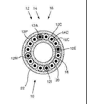
Reference is now made to Figs. 1A and 1B, which are
schematic views of cabling 10, according to an embodiment of
the present invention. Fig. 1A is a schematic cross-
sectional view of the cabling. Fig. 1B is a schematic, side
view of cabling 10, which has been partially cut-away to
expose internal elements of the cabling. As is explained
further below, an electrode is attached to the cabling, and
the cabling is typically configured so that a large number
of separate electrodes, each having respective attached
wires, may be attached in a small length of the cabling, so
that cabling 10 is capable of supporting a high density of
electrodes. Cabling 10 is typically used as part of a
medical catheter wherein electrical measurements are to be
made from the electrodes attached to the cabling.
Cabling 10 comprises a plurality of generally similar
wires 12, each wire 12 being formed as a conductor 14
covered by an insulating layer 16. In the following
description, generally similar components associated with
cabling 10 are referred to generically by their identifying
component numeral, and are differentiated from each other,
as necessary, by appending a letter A, B, ... to the numeral.
Thus wire 12C is formed as conductor 14C covered by
insulating layer 16C. While embodiments of the present
invention may be implemented with substantially any
plurality of wires 12 in the cabling, for clarity and
simplicity in the following description cabling 10 is
assumed to comprise 16 wires 12A, ... 12E, ... 121, ... 12M, ...
12P.
(For purposes of illustration, insulating layers 16 of
wires 12 have been drawn as having approximately the same
dimensions as conductors 14. In practice, the insulating
5
CA 02865334 2014-09-26
layer is typically approximately one-tenth the diameter of
the wire.)
In order to be used as part of a medical catheter, an
outer diameter of cabling 10 is implemented to be as small
as possible. In one embodiment, cabling 10 is approximately
cylindrical with a length of approximately 2 m, and an outer
diameter approximately equal to 0.5 mm.
Wires 12 may be formed with any diameter wire that is
consistent with the outer diameter of cabling 10. In one
embodiment wires 12 are formed of 48 AWG wire, corresponding
to a wire diameter of approximately 30 microns. In some
embodiments of the present invention the inventors have
used, inter alia, monel, constantan, or copper for
conductors 14. While copper has a higher electrical
conductivity than monel or constantan, it may have a
tendency to break during production of the cabling. Both
monel and constantan enhance the strength of cabling 10, but
in environments where magnetic properties of materials are
significant, such as during a magnetic resonance imaging
procedure or in a catheter using magnetic navigation, it may
be preferable to use constantan for conductors 14.
While monel, constantan and copper are provided as
examples of the material used for conductors 14, it will be
understood that embodiments of the present invention are not
limited to a particular type of material, and any other
convenient electrically conducting material may be used. In
some embodiments wires that neighbor each other may be
selected to have dissimilar conductors, such as copper and
constantan, so as to be available for forming a thermocouple
junction.
Wires 12 are formed over an internal core 18, which is
typically shaped as a cylindrical tube, and core 18 is also
referred to herein as tube 18. The core material is
typically selected to be a thermoplastic elastomer such as a
6
CA 02865334 2014-09-26
polyether block amide (PEBA). In a disclosed embodiment core
18 is formed of 401) Pebax, produced by Arkema, Colombes,
France. In the disclosed embodiment core 18, by way of
example, is cylindrical with a wall thickness of
approximately 13 microns, and an outer diameter of
approximately 0.4 mm. Wires 12 are formed on an outer
surface 20 of core 18 by coiling the wires around the tube.
Thus, in the case that core 18 is cylindrical, each wire 12
on the outer surface is in the form of a helical coil. In
contrast to a braid, all helical coils of wires 12 have the
same handedness, i.e., all wires of the cabling are left-
handed, or all wires of the cabling are right-handed. In the
present disclosure and in the claims, cabling, wherein all
the wires of the cabling that are coiled around an internal
core of the cabling have the same handedness, is referred to
as single-handed cabling. Also in the present disclosure and
in the claims, cabling wherein the wires of the cabling
comprise a first group of wires coiled left-handedly and a
second group of wires coiled right-handedly, is referred to
as braided cabling. Typically in braided cabling the number
of wires in the first group equals the number in the second
group.
Further details of a single-handed cabling generally
similar to cabling 10 are provided in U.S. Patent
Application Number 13/860,921, referenced above. An example
of a braided cabling is provided in U.S. Patent Application
2012/0172714, referenced above.
For simplicity, the following description considers
only single-handed cabling, as is exemplified by cabling 10.
However, embodiments of the present invention apply to
either single-handed or braided cabling, and those having
ordinary skill in the art will be able to adapt the
description, mutatis mutandis, for braided cabling.
7
CA 02865334 2014-09-26
In coiling wires 12 on surface 20, the wires are
typically arranged so that they contact each other in a
"close-packed" configuration. In other words, if internal
tube 18 were to be opened so that surface 20 is a flat
plane, the wires (neglecting "end-effects") form a single
wire layer over surface 20, with insulating layers 16
continuously in contact with two other insulating layers,
and with the insulating layers being continuously in contact
with surface 20.
In the case of tube 18 being cylindrical, the close-
packed arrangement of the helical coils of wires 12 means
that the wires are configured in a multi-start thread
configuration. Such a configuration is described in more
detail in U.S. Patent Application Number 13/860,921
referenced above.
Once wires 12 have been formed in the multi-start
thread configuration described above, the wires are covered
with a protective sheath 22. The protective sheath material
is typically selected to be a thermoplastic elastomer such
as PEBA. In a disclosed embodiment sheath 22 is formed of
55D Pebax, produced by Arkema, and no additives are
incorporated in the sheath, so that it is transparent. In
the disclosed embodiment sheath 22, by way of example, has
an outer diameter of approximately 0.5 mm.
Typically, although not necessarily, the insulating
layer of at least one of wires 12 is colored differently
from the colors of the remaining wires. Such coloration aids
in identifying particular wires once they have been arranged
within cabling 10, assuming that sheath 22 is transparent.
An alternative method for identifying particular wires in a
braided arrangement is described in U.S. Patent Application
2012/0172714.
By way of example, in the embodiment described herein,
using 16 wires, every fourth wire has its insulating layer
8
CA 02865334 2014-09-26
colored, so that insulating layers 16A, 16E, 161, and 16M
are respectively colored green, black, red, and violet. The
insulating layers of the remaining wires may be given
another color, such as white, or may be left colorless.
Thus, wires 12A, 12E, 121, and 12M appear to have the colors
green, black, red, and violet, and are visually different in
appearance from the remaining wires.
The process of coiling wires 12 around a core, and then
covering the wires by a sheath, essentially embeds the wires
within a wall of cabling 10, the wall consisting of the core
and the sheath. Embedding the wires within a wall means that
the wires are not subject to mechanical damage when the
cabling is used to form a catheter. Mechanical damage is
prevalent for small wires, such as the 48 AWG wires
exemplified above, if the wires are left loose during
assembly of a catheter.
Figs. 2A - 2E are schematic diagrams illustrating steps
in attaching electrodes 64 to cabling 10, and Fig. 3 is a
flowchart 100 describing the steps, according to embodiments
of the present invention. Typically, up to 16 electrodes 64,
i.e., electrodes 64A, 64B, ... 640, 64P, may be attached to
respective wires of the cabling. The following description
refers to a specific electrode by the generic term electrode
64.
Fig. 2A is a schematic top view of the cabling and
Figs. 2B - 2E are schematic side views of the cabling in
different stages of the attachment of electrode 64. In all
views parts of sheath 22 have been cut-away to expose wires
12 of cabling 10, as well as to illustrate the attachment of
electrode 64 to the cabling.
Electrode 64 is typically in the form of a conductive
ring with dimensions enabling it to be slid over sheath 22.
More details of alternative shapes for electrode 64 are
provided below. The following explanation assumes that the
9
CA 02865334 2014-09-26
electrode is to be attached to conductor 14E of colored wire
12E at a distal end of cabling 10.
In an initial step 102 a location for attaching the
electrode is selected by first finding colored wire 12E
visually, and then finding a required location for the
electrode along the cabling. The visual determination is
possible since sheath 22 is transparent.
In an access step 104 a section of sheath 22 above the
wire, and a corresponding section of insulating layer 16E,
are removed. The removal provides an access channel 42,
through the insulation of sheath 22 and also through the
insulation of layer 16E, to a section 46 of conductor 14E,
as is illustrated in Fig. 2A. The removal of the insulation,
which exposes the section of conductor 14E, may be by any
convenient means, such as by using a laser to penetrate the
insulation, or by mechanical removal of the insulation.
In a glue application step 106, glue 44 is applied over
the access channel. The application of the glue typically
covers channel 42, as is illustrated in Fig. 2B.
In a solder ball step 108, a solder ball 60 is
positioned in proximity to the entrance of access channel
42, and is held in place relative to the channel by glue 44.
The positioning of the solder ball is illustrated in Fig.
2C.
Typically, solder ball 60 is formed from a low melting
point metal, or a low melting point alloy. In one embodiment
of the present invention, solder ball 60 is formed from
indium.
In an electrode positioning step 110, electrode 64 is
located to be in contact with the solder ball. By way of
example electrode 64 is assumed to be in the form of a ring,
and is also referred to herein as ring electrode 64. In some
embodiments ring electrode 64 completely encircles cabling
10, in which case the positioning of ring electrode 64 may
CA 02865334 2014-09-26
be implemented by sliding the ring along cabling 10 so that
the ring covers the solder ball. In alternative embodiments
ring electrode 64 partially encircles cabling 10, as a
"broken" ring, in which case the positioning of ring
electrode 64 may be implemented by pushing the ring over
cabling 10 so that the ring covers the solder ball. In the
remaining description of the flowchart, ring electrode 64 is
assumed to completely encircle the cabling. The positioning
of ring electrode 64, for a completely encircling ring, to
cover the solder ball is illustrated in Fig. 21J.
In a heating step 112 ring electrode 64 is heated, and
while being heated is pressed onto ball 60. The combination
of heat and pressure melts the solder of the ball so that
the ball deforms, and so that the molten solder wets the
inner surface of ring electrode 64 and also penetrates
channel 42. The molten solder penetrating the channel wets
the exposed section of conductor 14E.
In a final step 114, the heating applied to the ring
electrode is removed, and the electrode and solder are
allowed to cool, typically to ambient room temperature. On
cooling, the solder solidifies into a solid solder bridge
68, as is illustrated in Fig. 2E. Bridge 68, which
corresponds to a deformed solder ball, connects electrode 64
and section 46 of conductor 14E.
Fig. 4 is a schematic illustration of an invasive
medical procedure using cabling 10, according to an
embodiment of the present invention. In preparation for the
procedure, cabling 10 is incorporated into a catheter 150,
the cabling having electrodes 64 at its distal end. Catheter
150 uses one set of cabling 10, and is typically a catheter
that is used for measuring electrical properties of a body
cavity. At its distal end catheter 150 may be straight or
curved as a lasso or helical catheter.
11
CA 02865334 2014-09-26
By way of example, a medical professional 156 is
assumed to insert catheter 150 into a patient 158 in order
to acquire electropotential signals from a heart 160 of the
patient. The professional uses a handle 162 attached to the
catheter in order to perform the insertion, and signals
generated at electrodes 64 are conveyed to a console 164.
Console 164 comprises a processing unit 166 which
analyzes the received signals, and which may present results
of the analysis on a display 168 attached to the console.
The results are typically in the form of a map, numerical
displays, and/or graphs derived from the signals.
A more detailed description of the use of a catheter
such as catheter 150 in acquiring electropotentials is
provided in U.S. Patents 6,584,345 and 6,400,981, both to
Govari, which are incorporated herein by reference.
While the description above has been generally directed
to attaching an electrode to cabling having wires coiled in
a single-handed manner, it will be appreciated that the
scope of the present invention includes cabling that is
braided, i.e., wherein the cabling comprises wires formed as
both left- and right-handed coils. It will also be
appreciated that the electrode attached to the cabling need
not be in the form of a ring encircling the cabling, but
rather may be any convenient shape that does not encircle
the cabling.
It will thus be appreciated that the embodiments
described above are cited by way of example, and that the
present invention is not limited to what has been
particularly shown and described hereinabove.
Rather, the
scope of the present invention includes both combinations
and subcombinations of the various features described
hereinabove, as well as variations and modifications thereof
which would occur to persons skilled in the art upon reading
12
CA 02865334 2014-09-26
. .
the foregoing description and which are not disclosed in the
prior art.
13