Note: Descriptions are shown in the official language in which they were submitted.
CA 02865604 2014-08-26
DESCRIPTION
Title of Invention
MANUFACTURING METHOD AND MANUFACTURING DEVICE FOR OPTICAL
SUBSTRATE HAVING CONCAVO-CONVEX PATTERN USING FILM-SHAPED
MOLD, AND MANUFACTURING METHOD FOR DEVICE PROVIDED WITH
OPTICAL SUBSTRATE
Technical Field
[0001] The present invention relates to a manufacturing method for
manufacturing an
optical substrate having a minute or fine concave and convex pattern (concavo-
convex
pattern) for scattering or diffracting light, by using a long film-shaped
mold; an apparatus
performing the manufacturing method; and a method for manufacturing a device
provided
with the optical substrate produced by the manufacturing method.
Background Art
[0002] There has been known a lithography method as a method for forming a
minute
pattern such as a semiconductor integrated circuit. The resolution of the
pattern formed
by the lithography method is dependent on the wavelength of a light source and
the
numerical aperture of an optical system, and the light source is expected to
have shorter
wavelength in order to meet demand for miniaturized devices in recent years.
However,
the light source having the short wavelength is expensive, development thereof
is not easy,
and the development of an optical material transmitting such a short-
wavelength light is
also needed. Further, manufacturing a large-area pattern through a
conventional
lithography method needs a large-size optical element, and thus there are
difficulties in
technical and economic aspects. Therefore, a novel method for forming a
desired pattern
on a large area has been studied.
[0003] There has been known a nanoimprint method as a method for forming a
minute
pattern without using any conventional lithography apparatus. The nanoimprint
method
is a technique such that a pattern of an order of nanometer can be transferred
by
sandwiching a resin between a mold and a substrate. A thermal nanoimprint
method, a
photonanoimprint method, and the like have been studied depending on the
employed
material. Of the above methods, the photonanoimprint method includes four
steps of: i)
1
CA 02865604 2014-08-26
resin coating (application of a resin layer); ii) pressing by use of the mold;
iii)
photo-curing; and iv) mold-releasing. The photonanoimprint method is excellent
in that
processing on a nanoscale can be achieved by the simple process as described
above.
Especially, since a photo-curable resin curable by being irradiated with light
is used as the
resin layer, a period of time for a pattern transfer step is short and high
throughput is
promised. Thus, the photonanoimprint method is expected to come into practical
use in
many fields including, for example, an optical member such as an organic EL
element
(Organic Electro-Luminescence element or organic light emitting diode) and
LED, MEMS,
and a biochip, in addition to a semiconductor device.
[0004] For example, in the organic EL element (organic light emitting diode),
a hole
injected from a hole injecting layer and electron injected from an electron
injecting layer
are carried to a light emitting layer respectively, then the hole and electron
are recombined
on an organic molecule in the light emitting layer to excite the organic
molecule, and
thereby light emission occurs. Therefore, in a case that the organic EL
element is used as
a display device and/or an illumination device, the light from the light
emitting layer is
required to be efficiently extracted from the surface of the organic EL
element. In order
to meet this demand, PATENT LITERATURE 1 discloses that a diffraction-grating
substrate is provided on a light extraction surface of the organic EL element.
Citation List
Patent Literature
[0005] PATENT LITERATURE 1: Japanese Patent Application Laid-open No.
2006-236748
PATENT LITERATURE 2: PCT International Publication No.
W02011/007878A1
[0006] The applicant of the present invention discloses the following method
in PATENT
LITERATURE 2 in order to manufacture a concave and convex pattern of the
diffraction
grating substrate for the organic EL element. That is, a solution obtained by
dissolving a
block copolymer satisfying a predetermined condition into a solvent is applied
on a base
member to form a micro phase separation structure of the block copolymer by
using a
self-organizing phenomenon of the block copolymer, and thereby obtaining a
master block
(metal substrate) in which a minute or fine and irregular concave and convex
pattern is
formed. A mixture of a silicon-based polymer and a curing agent is dripped
onto the
2
CA 02865604 2016-06-02
obtained master block and then cured to obtain a transferred pattern as a
mold. Then, a
glass substrate coated with a curable resin is pressed against the transferred
pattern and the
curable resin is cured by irradiation with ultraviolet rays. In this way, a
diffraction grating
in which the transferred pattern is duplicated is manufactured. The organic EL
element
can be obtained by stacking a transparent electrode, an organic layer, and a
metal electrode
on the diffraction grating.
[0007] However, in order to mass-produce the above-mentioned diffraction
grating for
the organic EL element, it is necessary to efficiently perform the pattern
transfer (pattern
formation) onto the material such as the curable resin by using the
transferred pattern of
the mold.
[0008] Thus, it is expected to develop a new transfer process and transfer
apparatus
which are capable of mass-producing the optical substrate, such as the
diffraction-grating
substrate, used for the organic EL element and the like with high throughput
by using the
nanoimprint method.
[0009] The photo-curable resin described above generally has low heat
resistance, and is
decomposed and/or turns into yellow at high temperature. Thus, there is fear
that a film
having the minute pattern might be broken in a case that a high-temperature
treatment is
included in subsequent steps. Further, the photo-curable resin has a low
adhesion
property to a glass substrate. Furthermore, in a case that the resin layer to
which the
pattern has been transferred is used for an element such as the organic EL
element, there is
fear that impurities are eluted from the resin layer to cause adverse effect
on the element.
Therefore, in order to mass-produce the optical substrate, such as the
diffracting-grating
substrate, for the organic EL element with high throughput by using the
nanoimprint
method, the material for forming the concave and convex pattern on the glass
substrate
and/or mold material are required to be optimized.
Summary of Invention
Technical Problem
[0010] In view of the above, an object of the present invention is to provide
a novel
manufacturing method and manufacturing apparatus capable of mass-producing an
optical
substrate and a device provided with the optical substrate with high
throughput, the optical
substrate including a minute or fine concave and convex pattern which has a
high adhesion
property to a substrate, heat resistance, and weather resistance.
3
CA 02865604 2014-08-26
Solution to the Problem
[0011] According to a first aspect of the present invention, there is provided
a method for
manufacturing an optical substrate having a concave and convex pattern,
including:
a step of preparing a long film-shaped mold having a surface of the concave
and
convex pattern;
a step of forming a coating film made of a sol-gel material on a substrate;
a step of transferring the surface of the concave and convex pattern of the
film-shaped mold to the coating film by arranging the surface of the concave
and convex
pattern to face the coating film and pressing a pressing roll against a
surface of the
film-shaped mold on a side opposite to the surface of the concave and convex
pattern;
a step of releasing the film-shaped mold from the coating film; and
a step of curing the coating film to which the concave and convex pattern has
been
transferred.
[0012] In the method for manufacturing the optical substrate, the step of
curing the
coating film may include curing the coating film by baking the coating film.
[0013] In the method for manufacturing the optical substrate, the step of
preparing the
long film-shaped mold may include:
coating a long film-shaped base member with a concave-convex forming material;
performing a roll transfer of the concave and convex pattern to the
concave-convex forming material by pressing a transfer roll having the concave
and
convex pattern against the concave-convex forming material coating the long
film-shaped
base member while rotating the transfer roll; and
curing the concave-convex forming material to which the concave and convex
pattern has been transferred through the roll transfer so as to obtain the
long film-shaped
mold in a roll shape. Further,
the film-shaped base member having the cured
concave-convex forming material may be wound around a film winding roll,
and/or the
concave and convex pattern of the transfer roll may be transferred while the
film-shaped
base member is transported by using a film feeding roll feeding the film-
shaped base
member and the film winding roll winding or rolling up the film-shaped base
member. In
any case, the long film-shaped mold in the roll shape wound around the film
winding roll
may move with being fed to the pressing roll. The released long film-shaped
mold may
be wound around a mold winding roll.
4
CA 02865604 2014-08-26
[0014] In the method for manufacturing the optical substrate, the pressing
roll may be
pressed against the surface of the film-shaped mold on the side opposite to
the surface of
the concave and convex pattern while the coating film being heated. By doing
so, the
pre-baking of the sol-gel material is performed simultaneously with the
pressing, which
makes it possible to form the concave and convex pattern reliably and to
facilitate the
releasing of the surface of the concave and convex pattern from the coating
film after the
pressing. Further, it is possible to further facilitate the releasing of the
surface of the
concave and convex pattern from the coating film after the pressing by heating
the pressed
coating film in the releasing step or between the transfer step and the
releasing step.
[0015] In the method for manufacturing the optical substrate, the surface of
the concave
and convex pattern of the long film-shaped mold may be successively pressed
against
coating films on a plurality of substrates with the pressing roll while
continuously feeding
the long film-shaped mold under or below the pressing roll and transporting
each of the
substrates to the pressing roll at a predetermined time interval with the
coating film made
of the sol-gel material being formed. The use of the long film-shaped mold
enables the
continuous process of each of the substrates, thereby making it possible to
improve the
throughput of manufacture of the optical substrate. The length of the film-
shaped mold
can be adjusted to a length enough to produce the optical substrate in amount
of one lot, for
example, hundreds to thousands of optical substrates. For example, the length
of the
film-shaped mold can be adjusted in a range of several hundreds of meters to
several
thousands of meters.
[0016] The concave and convex pattern of the film-shaped mold used in the
method for
manufacturing the optical substrate may be, for example, an irregular concave
and convex
pattern in which an average pitch of concavities and convexities is in a range
of 100 to
1500 nm and an average value (average height) of a depth distribution of the
concavities
and convexities is in a range of 20 to 200 nm.
[0017] According to a second aspect of the present invention, there is
provided an
apparatus for manufacturing an optical substrate, including:
a coating-film forming section configured to form a coating film made of a sol-
gel
material on a substrate;
a substrate transporting section configured to transport the substrate on
which the
coating film is formed to a predetermined position;
CA 02865604 2016-06-02
a mold transporting section which includes a mold feeding roll configured to
feed
a long film-shaped mold having a surface of a concave and convex pattern and a
mold
winding roll configured to wind or roll up the long film-shaped mold, and is
configured to
transport the film-shaped mold to the predetermined position by continuously
feeding the
film-shaped mold from the mold feeding roll to the predetermined position and
winding
the film-shaped mold around the mold winding roll; and
a pressing roll rotatably arranged at the predetermined position and
configured to
press a part of the surface of the concave and convex pattern of the long film-
shaped mold,
which is fed to the predetermined position by the mold transporting section,
against the
coating film on the substrate which is transported to the predetermined
position by the
substrate transporting section.
[0018] The apparatus for manufacturing the optical substrate may further
include a
peeling roll configured to peel (release) the part of the surface of the
concave and convex
pattern of the long film-shaped mold pressed with the pressing roll from the
coating film
on the substrate.
[0019] The apparatus for manufacturing the optical substrate may further
include a
heating means configured to heat the coating film on the substrate against
which the part of
the surface of the concave and convex pattern of the film-shaped mold is
pressed. The
heating means may be provided in the pressing roll. The apparatus for
manufacturing the
optical substrate may further include a heating means configured to heat the
coating film
when the film-shaped mold is released (peeled off) from the coating film.
[0020] The apparatus for manufacturing the optical substrate may further
include a
supporting roll provided at a position to face the pressing roll and
configured to support the
substrate from a lower side of the substrate. The coating-film forming section
may
include a substrate stage configured to move the substrate while holding the
substrate.
[0021] The concave and convex pattern of the film-shaped mold used in the
apparatus for
manufacturing the optical substrate may be, for example, an irregular concave
and convex
pattern used for scattering or diffracting light in which an average pitch of
concavities and
convexities is in a range of 100 to 1500 nm and an average value (average
height) of a
depth distribution of the concavities and convexities is in a range of 20 to
200 nm.
[0022] The apparatus for manufacturing the optical substrate may further
include a roll
process apparatus configured to form the long film-shaped mold, the roll
process apparatus
including: a transporting system configured to transport a substrate film; a
coating unit
6
CA 02865604 2016-06-02
configured to coat the substrate film being transported with a concave-convex
forming
material; a transfer roll provided on a downstream side of the coating unit
and configured
to transfer the concave and convex pattern to the concave-convex forming
material; and a
radiation light source configured to emit light to the substrate film. The
transporting
system may include a film feeding roll configured to feed the substrate film;
a nip roll
configured to urge the substrate film toward the transfer roll; a releasing
roll configured to
facilitate releasing of the substrate film from the transfer roll; and a film
winding roll
configured to wind or roll up the substrate film to which the concave and
convex pattern
has been transferred. In this case, the film winding roll around which the
substrate film is
wound may be used as the mold feeding roll configured to feed the film-shaped
mold.
[0023] According to a third aspect of the present invention, there is provided
a method
for manufacturing a device provided with an optical substrate having a concave
and
convex pattern, including:
a substrate formation step of forming a substrate with a predetermined concave
and convex pattern by coating the substrate with a sol-gel material and
transferring the
concave and convex pattern to the sol-gel material coating the substrate;
a cleaning step of cleaning the substrate with the concave and convex pattern;
a first electrode formation step of forming a first electrode on the cleaned
substrate by patterning;
an annealing step of annealing the substrate in which the first electrode is
formed;
a thin film formation step of forming a thin film on the first electrode; and
a second electrode formation step of forming a second electrode on the thin
film.
[0024] In the method for manufacturing the device of the present invention,
the sol-gel
material as a transfer-target material of the concave and convex pattern has
corrosion
resistance and high strength as compared with resin material. Thus, ultrasonic
cleaning,
cleaning with a brush, and/or UV/03 cleaning may be performed in the cleaning
step.
[0025] In the method for manufacturing the device of the present invention,
the
patterning may be performed by using an acid solvent or an alkaline solvent,
and the
patterning may include formation of a first electrode layer, resist coating
(application of a
resist), exposure and development, etching of the first electrode layer, and
stripping
(removing) of the resist. The sol-gel material also has the corrosion
resistance to the
solvent used for each of the processes.
[0026] In the method for manufacturing the device of the present invention,
since the
7
CA 02865604 2016-06-02
sol-gel material as the transfer-target material of the concave and convex
pattern has heat
resistance, the annealing may be performed at a temperature in a range of 160
degrees
Celsius to 360 degrees Celsius.
[0027] The method for manufacturing the device of the present invention is
suitable for
the manufacture of an organic EL element as the device. In this case, the
first electrode
may be a transparent electrode, the thin film may include an organic layer,
and the second
electrode may be a metal electrode. Further, the method for manufacturing the
device of
the present invention is suitable for the manufacture of a solar cell as the
device. In this
case, the first electrode may be a transparent electrode, the thin film may
include a
semiconductor layer, and the second electrode may be a metal electrode.
[0028] The concave and convex pattern used in the method for manufacturing the
device
of the present invention may be an irregular concave and convex pattern used
for scattering
or diffracting light in which an average pitch of concavities and convexities
is in a range of
100 to 1500 nm and an average value of a depth distribution of the concavities
and
convexities is in a range of 20 to 200 nm. The substrate may be a glass
substrate and the
sol-gel material may include a silica precursor. The method for manufacturing
the device
of the present invention may further include baking of the sol-gel material at
a temperature
of 300 degrees Celsius or more after coating the substrate with the sol-gel
material and
transferring the predetermined concave and convex pattern to the sol-gel
material coating
the substrate.
[0029] In the method for manufacturing the device of the present invention,
the substrate
formation step may include:
a step of preparing a long film-shaped mold having a surface of the concave
and
convex pattern;
a step of forming a coating film made of the sol-gel material on the
substrate;
a step of transferring the surface of the concave and convex pattern of the
film-shaped mold to the coating film by arranging the surface of the concave
and convex
pattern of the film-shaped mold to face the coating film and pressing a
pressing roll against
a surface of the film-shaped mold on a side opposite to the surface of the
concave and
convex pattern;
a step of releasing (peeling) the film-shaped mold from the coating film; and
a step of baking the coating film to which the concave and convex pattern has
been transferred.
8
CA 02865604 2016-06-02
Advantageous Effects of Invention
[0030] In the method for manufacturing the optical substrate of the present
invention,
since the sol-gel material is used as the concave-convex pattern forming
material and the
roll process with the long film-shaped mold is utilized to form the concave
and convex
pattern made of the sol-gel material, it is possible to manufacture the
optical substrate with
high throughput while performing the pattern transfer accurately and reliably.
Since the
concave and convex pattern of the optical substrate manufactured by the method
for
manufacturing the optical substrate of the present invention is made of the
sol-gel material,
the optical substrate with the concave and convex pattern is excellent in heat
resistance,
weather resistance (of which concept includes light resistance), and corrosion
resistance.
Further, the optical substrate with the concave and convex pattern is also
resistant to the
manufacturing process of an element in which the optical substrate is
incorporated, which
makes it possible to extend the service life of the element.
[0031] Since the long film-shaped mold is utilized in the present invention,
there are
advantages as follows. That is, regarding a hard mold made of metal, silica,
and the like,
in a case that any defect has been found in a concave and convex pattern of
the hard mold,
it is possible to clean and/or repair the defect. Thus, any failure can be
avoided which
would be otherwise caused by the transfer of the defect to the sol-gel
material layer.
However, in the film-shaped mold, the cleaning and the repair as described
above are less
likely to be performed easily. In the meanwhile, the mold made of metal,
silica, and the
like is in a roll shape, and when any defect such as clogging occurs in the
mold, a transfer
device is required to be immediately stopped to exchange the mold. However,
since the
transfer using the film-shaped mold is performed while each of the parts of
the film-shaped
mold being made to correspond to each single glass substrate, a part having
the defect such
as the clogging is marked at an inspection stage, and the transport of the
glass substrate can
be suspended until the defect part passes through the glass substrate.
Therefore, on the
whole, the use of the film-shaped mold can reduce the occurrence of defective
product and
thereby making it possible to improve the throughput. In a case that the
concave and
convex pattern of the hard mold made of metal, silica, and the like is tried
to be directly
transferred to the sol-gel material layer, various limitations as described
below arise and
thereby a desired performance can not be given sufficiently in some cases. For
example,
in a case that a hard substrate such as glass is used as the substrate on
which the sol-gel
9
CA 02865604 2014-08-26
material layer is formed, the adjustment of the pressure applied to the mold
is difficult.
For example, if the pressure applied to the mold is high, the substrate is
damaged, for
example, to have a crack since both of the substrate and the mold are hard; or
if the
pressure applied to the mold is low, the concave and convex pattern is
transferred
insufficiently. Therefore, a soft material must be used for the substrate or
the mold.
Even when the film-shaped mold (soft mold) is used, a material to which the
concave and
convex pattern is transferred is required to have a superior mold-releasing
property, a
superior adhesion property to the substrate, and a superior transferability of
the concave
and convex pattern. Thus, the material must be selected from among limited
materials.
Accordingly, by dividing the method for manufacturing the optical substrate
into two steps
including the first step of manufacturing the film-shaped mold from the metal
mold and the
second step of performing the transfer to the sol-gel material layer with the
film-shaped
mold, and by selecting a material suitable for each of the steps, a desired
material can be
used on a desired substrate in the optical substrate. Consequently, the
transfer can be
performed to have a satisfactory mold-releasing property without causing any
pattern
defect, while satisfying necessary characteristics.
[0032] In the method for manufacturing the device of the present invention,
since the
concave and convex pattern of the optical substrate is made of the sol-gel
material, the
optical substrate has the resistance to the cleaning with the brush and the
UV/03 cleaning
in the cleaning step of cleaning the substrate with the concave and convex
pattern, the
corrosion resistance to the acid solvent or alkali solvent used in the first
electrode
formation step, and the heat resistance to high temperature in the subsequent
annealing step.
Therefore, it is possible to produce the device without inhibiting optical
characteristics of
the optical substrate with the concave and convex pattern and/or an adhesion
property to
the thin film, which is formed as a working layer, on the optical substrate.
Further, the
method for manufacturing the device of the present invention also contributes
to improve
the heat resistance, the weather resistance, and the corrosion resistance of
the device itself
manufactured by the method for manufacturing the device of the present
invention.
Accordingly, the method for manufacturing the device of the present invention
is
extremely useful when manufacturing various devices such as the organic EL
element and
the solar cell with high throughput.
Brief Description of Drawings
CA 02865604 2014-08-26
[0033]
Fig. 1 is a flowchart showing a method for manufacturing a device of the
present
invention.
Fig. 2 is a flowchart showing manufacturing steps of an optical substrate used
for
the method for manufacturing the device of the present invention.
Fig. 3 is a conceptual view of a roll process apparatus for manufacturing a
film-shaped mold used for manufacture of the optical substrate.
Fig. 4 is a conceptual view for illustrating a roll process using the film-
shaped
mold.
Figs. 5(a) to 5(t) conceptually show a process for manufacturing an ITO
transparent electrode.
Fig. 6 shows a cross-section structure of an organic EL element.
Fig. 7 is a conceptual view of an optical substrate manufacturing apparatus
for
performing a method for manufacturing the optical substrate of the present
invention.
Fig. 8 is a conceptual view illustrating a modified embodiment of the optical
substrate manufacturing apparatus, in which no peeling roll is utilized.
Fig. 9 is a conceptual view illustrating another modified embodiment of the
optical substrate manufacturing apparatus, in which the film-shaped mold as an
endless
belt is utilized.
Fig. 10 is a conceptual view illustrating still another modified embodiment of
the
optical substrate manufacturing apparatus, in which a heat zone as a heating
means of a
sol-gel material layer is provided in a pressing section.
Fig. 11 is a conceptual view illustrating an apparatus for inspecting
unevenness of
a diffraction grating substrate.
Fig. 12(a) is a photograph showing an image from the surface of the substrate
observed in Example 1, and Fig. 12(b) is a graph showing profile of pixel
positions on the
line LI in the photograph of Fig. 12(a) and pixel values at the pixel
positions.
Description of Embodiments
[0034] In the following, embodiments of the present invention will be
described with
reference to the drawings. As shown in Fig. 1, a method for manufacturing a
device
provided with an optical substrate having a concave and convex pattern
according to the
present invention mainly includes: a substrate formation step P1 for forming a
substrate in
11
CA 02865604 2014-08-26
which the concave and convex pattern is formed; a cleaning step P2 for
cleaning the
substrate in which the concave and convex pattern is formed; a first electrode
formation
step P3 for forming a first electrode on the cleaned substrate by patterning
using an acid
solvent or alkaline solvent; an annealing step P4 for annealing the substrate,
on which the
patterned first electrode is formed, at a predetermined temperature; a thin
film formation
step P5 for forming a thin film on the annealed substrate; and a second
electrode formation
step S6 for forming a second electrode on the thin film. The substrate
formation step PI
for forming the substrate in which the concave and convex pattern is formed
includes a
method for manufacturing the optical substrate having the concave and convex
pattern
according to the present invention. As shown in Fig. 2, the method for
manufacturing the
optical substrate having the concave and convex pattern mainly includes a step
SO for
preparing a film-shaped mold; a solution preparation step SI for preparing a
sol-gel
material; a coating step S2 for coating a substrate with the prepared sol-gel
material
(applying the prepared sol-gel material on a substrate); a drying step S3 for
drying the
coating film of the sol-gel material coating the substrate; a transfer step S4
for pressing the
film-shaped mold in which a transfer pattern is formed against the dried
coating film with a
pressing roll; a releasing step (peeling step) S5 for releasing (peeling off)
the mold from
the coating film; and a main baking step S6 in which the coating film is
subjected to main
baking.
[0035] Hereinbelow, the method for manufacturing the optical substrate and the
method
for manufacturing the device including the optical substrate manufactured by
this
manufacturing method according to the present invention will be explained by
citing a
manufacturing process of an organic EL element 200 as shown in Fig. 6, as an
example,
the organic EL element 200 including a stacked structure on a substrate
(diffraction grating
substrate) 40 having a sol-gel material layer 42 in which a concave and convex
pattern is
formed.
[0036]
[Substrate formation step]
At first, an explanation will be made about a method for manufacturing the
substrate 40 including the sol-gel material layer 42 in which the concave and
convex
pattern is formed using the method for manufacturing the optical substrate of
the present
invention by citing, as an example.
[0037]
12
CA 02865604 2014-08-26
<Step for preparing film-shaped mold>
The film-shaped mold used for manufacturing an optical member of the present
invention is a film-shaped or sheet-shaped mold which is long, flexible, and
has a concave
and convex transfer pattern on a surface thereof. The mold is made, for
example, of
organic materials such as silicone resin, polyethylene terephthalate (PET),
polyethylene
naphthalate (PEN), polycarbonate (PC), cycloolefin polymer (COP), polymethyl
methacrylate (PMMA), polystyrene (PS), polyimide (PI), and polyarylate. The
concave
and convex pattern may be formed directly in each of the materials, or may be
formed in
(on) a concave-convex forming material with which a base material (substrate
sheet)
formed of the above-mentioned materials is coated. It is possible to use photo-
curable
resin, thermosetting resin, and thermoplastic resin as the concave-convex
forming material.
[0038] The film-shaped mold is, for example, a long mold which may have 10
meter or
more in length, 50 to 3000 mm in width, and 1 to 500 gm in thickness. The size
of the
film-shape mold, in particular, the length thereof can be set appropriately
based on the size
of the optical substrate to be mass-produced, the number of optical substrates
(the number
of lots) continuously produced in a single manufacturing process. A surface
treatment or
an easy-adhesion treatment may be performed to improve an adhesion property
between
the substrate and the coating material (concave-convex forming material).
Further, a
mold-release treatment may be performed on each surface of the concave and
convex
pattern as needed. The concave and convex pattern may be formed to have any
profile by
arbitrary method.
[0039] The concave and convex pattern of the film-shaped mold varies in uses
of the
optical substrate finally obtained. The concave and convex pattern, for
example, may be
an irregular concave and convex pattern in which pitches of concavities and
convexities
are ununiform and orientations of the concavities and convexities have no
directivity. In
a case that the optical substrate is used for scattering or diffracting
visible light, for
example, the average pitch of the concavities and convexities can be within a
range from
100 to 1500 nm, and is more preferably within a range from 200 to 1500 nm. In
a case
that the average pitch of the concavities and convexities is less than the
lower limit, the
pitches are so small relative to wavelengths of the visible light that the
diffraction of light
by the concavities and convexities is likely to be insufficient. In a case
that the average
pitch exceeds the upper limit, a diffraction angle is so small that functions
as an optical
element such as the diffracting grating are more likely to be lost. In similar
uses, the
13
CA 02865604 2014-08-26
average value (average height) of a depth distribution of the concavities and
convexities is
preferably in a range of 20 to 200 nm, and more preferably in a range of 50 to
150 nm.
[0040] The light scattered and/or diffracted by such a concave and convex
pattern is not
light having single wavelength or wavelength having a narrow band. The light
scattered
and/or diffracted by such a concave and convex pattern has a range of
wavelength
relatively broad, has no directivity, and is directed in various directions.
However, the
"irregular concave and convex pattern" includes a quasi-periodic structure
such as that in
which a Fourier-transformed image, which is obtained by performing a two-
dimensional
fast Fourier-transform processing on a concavity and convexity analysis image
obtained by
analyzing a concave and convex shape on the surface, shows a circular or
annular pattern,
that is, such as that in which, although the concavities and convexities have
no particular
orientation, the pitches of the concavities and convexities vary. Therefore,
the substrate
having such a quasi-periodic structure is suitable for a diffraction substrate
used in a
surface-emitting element and the like such as the organic EL element; a
transparent
conductive substrate of a solar cell; and the like, provided that the
substrate has the
concavities and convexities of which pitch distribution or pitch variability
enables the
substrate diffract visible light.
[0041] An exemplary method for manufacturing the long film-shaped mold used in
the
present invention will be explained by referring to Fig. 3. A roll process
apparatus (first
unit) 70 shown in Fig. 3 is an apparatus for manufacturing the film-shaped
mold by
forming a concave and convex pattern on a coating film formed on a long
substrate film.
The roll process apparatus 70 mainly includes a transporting system 86 which
transports a
substrate film (base material) 80, a die coater 82 which coats the substrate
film 80 being
transported with the material for forming the concavities and convexities, a
transfer roll
(metal mold) 90 which is positioned on the downstream side of the die coater
82 and
transfers a pattern, and a radiation light source 85 which is provided to face
the transfer roll
90 with the substrate film 80 intervening therebetween and emits UV light to
the substrate
film 80. The transporting system 86 for transporting the substrate film 80
includes a film
feeding roll 72 which feeds the substrate film 80, a nip roll 74 which is
arranged to face the
transfer roll 90 with the substrate film 80 intervening therebetween, a
releasing roll
(peeling roll) 76 which facilitates the releasing (peeling) of the substrate
film 80 from the
transfer roll 90, a film winding roll 87 which winds or rolls up a substrate
film 80a
(film-shaped mold) having the pattern transferred thereon, and a plurality of
transporting
14
CA 02865604 2014-08-26
rolls 78 which transport the substrate film 80 while maintaining the tension
of the substrate
film 80.
[0042] The film-shaped mold is manufactured through the following
manufacturing
process by using the roll process apparatus 70. The substrate film 80 wound on
the film
feeding roll 72 in advance is fed to the downstream side by the rotations of
the film feeding
roll 72, the film winding roll 87, etc. When the substrate film 80 passes
through the die
coater 82, a concave-convex forming material 84 is applied on a surface of the
substrate
film 80 by the die coater 82 to form a coating film having a predetermined
thickness.
Then, the coating film on the substrate film 80 is pressed against the outer
circumferential
surface of the transfer roll 90 by the nip roll 74 so as to transfer a pattern
of the outer
circumferential surface of the transfer roll 90 to the coating film. At the
same time or
immediately after the above, UV light is emitted from the radiation light
source 85 to the
coating film so as to cure the concave-convex forming material 84. Although
the
wavelength of the UV light varies according to the concave-convex forming
material 84,
the wavelength of the UV light is generally in a range of 200 to 450 nm. The
amount of
irradiation may be in a range of 10 mJ/cm2 to 5 J/cm2. After releasing
(peeling off) the
substrate film 80 with the concave-convex forming material having the cured
pattern from
the transfer roll 90 by using the releasing roll (peeling roll) 76, the
substrate film 80 is
wound around the film winding roll 87. Accordingly, a long film-shaped mold
80a is
obtained. Since the long film-shaped mold 80a is obtained in a roll shape, it
is suitable
for a mass-producing process of the optical substrate using a pressing roll
which will be
described later. Further, the shape of the long film-shaped mold 80a is
suitable to be
transported to an apparatus performing the mass-producing process of the
optical substrate
by use of the pressing roll. Additionary, since the film-shaped mold is rolled
up it in a
roll shape after being manufactured, storage and aging processes can be easily
performed.
[0043] In the manufacturing process described above, the substrate film 80 is
exemplified,
for example, by base members made of inorganic materials such as glass; and
base members made of organic materials such as silicone resin, polyethylene
terephthalate (PET), polyethylene naphthalate (PEN), polycarbonate (PC),
cycloolefin
polymer (COP), polymethyl methacrylate (PMMA), polystyrene (PS), polyimide
(PI), and
polyarylate. The thickness of the substrate film may be, for example, in a
range of 1 to
500 gm.
[0044] The concave-convex forming material 84 is exemplified by curable resins
such as
CA 02865604 2014-08-26
various kinds of UV curable resins including, for example, epoxy resin,
acrylic resin,
methacrylic resin, vinyl ether resin, oxetane resin, urethane resin, melamine
resin, urea
resin, polyester resin, phenol resin, cross-linking type liquid crystal resin,
fluorine resin,
and silicone resin. The thickness of the curable resin is preferably in a
range of 0.5 to 500
Jim. In a case that the thickness is less than the lower limit, heights of the
concavities and
convexities formed on the surface of a cured resin layer are likely to be
insufficient. In a
case that the thickness exceeds the upper limit, the influence of volume
change of the resin
upon curing is likely to be so large that the formation of the shape of the
concavities and
convexities is liable to be unsatisfactory.
[0045] In the above manufacturing process, a die coating method by the die
coater is used
to coat the substrate film 80 with the concave-convex forming material 84
(apply the
concave-convex forming material 84 on the substrate film 80). Instead of this,
it is
possible to adopt various coating methods such as a spin coating method, a
spray coating
method, a dip coating method, a dropping method, a gravure printing method, a
screen
printing method, a relief printing method, a curtain coating method, an ink-
jet method, and
a sputtering method. The condition for curing the concave-convex forming
material 84
such as the curable resin varies depending on the kind of the resin used. For
example, a
curing temperature is preferably within a range from room temperature to 250
degrees
Celsius, and an UV light irradiation amount is preferably within a range from
10 mJ/cm2 to
J/cm2. The concave-convex forming material 84 may be cured by irradiation
with
energy rays such as electron beams other than the UV light.
[0046] The transfer roll 90 used in the above-mentioned manufacturing process
may be,
for example, a roll having a pattern directly formed on a surface thereof such
as a metal
roll; a roll in which a substrate having a pattern such as a metal substrate
is wound on the
roll and then fixed thereto; or a roll formed by manufacturing a cylindrical
substrate having
a pattern and fitting and fixing it to the roll. The transfer roll 90 may be
made of a hard
material other than the metal.
100471 Here, an explanation will be made about a method for forming a concave
and
convex pattern provided on the surface of the transfer roll 90. It is
preferred that the
concave and convex pattern be formed by a method of utilizing self-
organization or
assembly (micro phase separation) of a block copolymer described in Japanese
Patent
Application Laid-open No. 2011-006487 of the applicants of the present
invention
(hereinafter referred to as "BCP (Block Copolymer) method" as appropriate), a
method of
16
CA 02865604 2014-08-26
heating and cooling a polymer film on a vapor-deposited film to form
concavities and
convexities of wrinkles on a surface of polymer disclosed in PCT International
Publication
No. W02011/007878A1 of the applicants of the present invention (hereinafter
referred to
as "BKL (Buckling) method" as appropriate), or the like. A photolithography
method
may be utilized instead of the BCP and BKL methods. In a case that the pattern
is formed
by the BCP method, the pattern can be made of any material, and the material
is preferably
a block copolymer composed of combinations of two selected from the group
consisting of
a styrene-based polymer such as polystyren; polyalkyl methacrylate such as
polymethyl
methacrylate; polyethylene oxide; polybutadiene; polyisoprene;
polyvinylpyridine; and
polylactic acid.
[0048] Pitches and heights of concavities and convexities of the pattern are
arbitrary.
For example, in a case that the pattern is used as the diffraction grating
scattering or
diffracting light in a visible region, the average pitch of the concavities
and convexities is
preferably in a range of 100 nm to 1500 nm, more preferably in a range of 200
nm to 1500
nm. In a case that the average pitch of the concavities and convexities is
less than the
lower limit, the pitches are so small relative to wavelengths of the visible
light that the
diffraction of the light by the concavities and convexities is less likely to
occur. In a case
that the average pitch exceeds the upper limit, a diffraction angle is so
small that functions
as an optical element such as the diffraction grating are more likely to be
lost. The
average value of the depth distribution of the concavities and convexities is
preferably in a
range of 20 nm to 200 nm, and more preferably in a range of 50 nm to 150 nm.
In a case
that the average value of the depth distribution of the concavities and
convexities is less
than the lower limit, the height is so short relative to the wavelengths of
the visible light
that the required diffraction is less likely to occur. In a case that the
average value
exceeds the upper limit, the intensity of diffracted light becomes non-
uniform, and as a
result, the following tendency is found. When the concave and convex pattern
is used, for
example, as the optical element for light extraction of the organic EL
element, the electric
field distribution in an EL layer becomes non-uniform, and electric fields
concentrate on a
certain position or area, thereby a leak current is more likely to arise
and/or the service life
of the optical element is shortened.
[0049] After forming the master block with the pattern by the BCP or BKL
method, a
mold to which the pattern is transferred can be formed by an electroforming
method or the
like, as follows. At first, a seed layer functioning as an electroconductive
layer for an
17
CA 02865604 2014-08-26
electroforming process can be formed on the master block, which has the
pattern to be
transferred, formed by non-electrolytic plating, sputtering, vapor deposition,
or the like.
The thickness of the seed layer is preferably not less than 10 nm to
uniformize a current
density during the subsequent electroforming process, and thereby making the
thickness of
a metal layer accumulated by the subsequent electroforming process uniform. As
the
material of the seed layer, it is possible to use, for example, nickel,
copper, gold, silver,
platinum, titanium, cobalt, tin, zinc, chrome, gold-cobalt alloy, gold-nickel
alloy,
boron-nickel alloy, solder, copper-nickel-chromium alloy, tin-nickel alloy,
nickel-palladium
alloy, nickel-cobalt-phosphorus alloy, or alloy thereof. Subsequently, a metal
layer is
accumulated on the seed layer by the electroforming (electroplating). The
entire
thickness of the metal layer including the thickness of the seed layer can be,
for example,
in a range of 10 to 3000 pm. As the material of the metal layer accumulated by
the
electroforming, it is possible to use any of metal species as described above
which can be
used as the seed layer. It is preferable to use nickel as the material of the
metal layer in
view of the wear resistance, the releasing property, and the like of a metal
substrate to be
obtained as the mold. In this case, nickel is preferably used also for the
seed layer.
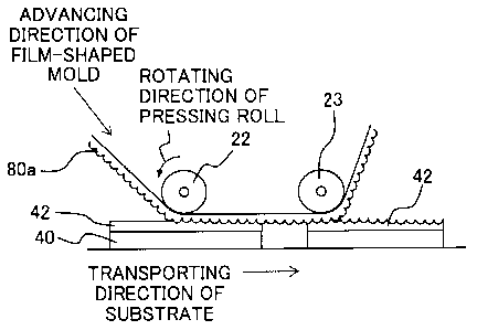
Considering ease of the subsequent processes for forming the mold such as
pressing to the
resin layer, releasing, and cleaning, the formed metal layer desirably has
appropriate
hardness and thickness.
[0050] The metal layer including the seed layer obtained as described above is
released
(peeled off) from the master block having the concave and convex structure to
obtain a
metal substrate. In order to release the metal layer easily and reliably, it
is preferred that
an annealing process be performed by heating the master block with the pattern
before the
electroforming. As the releasing method, the metal layer may be peeled off
physically, or
the materials composing the pattern of the master block may be dissolved to be
removed
by using an organic solvent dissolving them, such as toluene, tetrahydrofuran
(THF), and
chloroform. In a case that the metal substrate is peeled off from the master
block, a
remaining material component on the metal substrate can be removed by
cleaning. As the
cleaning method, it is possible to use wet cleaning using a surfactant etc.,
or dry cleaning
using ultraviolet rays and/or plasma. Alternatively, for example, the
remaining material
component may be attached to an adhesive agent or a bonding agent then be
removed.
Accordingly, the metal substrate to which the pattern has been transferred
from the master
block can be obtained. The transfer roll 90 having the concave and convex
pattern can be
18
CA 02865604 2014-08-26
obtained by winding or putting the metal substrate obtained as described above
around the
surface of a roll body. It is possible to form the film-shaped mold by using
the transfer
roll 90 by the above manufacturing process. It is needless to say that the
long
film-shaped mold is not required to be self-manufactured and a long film-
shaped mold
manufactured by a manufacturer such as a film manufacturer may be used. The
step for
preparing the film-shaped mold may be performed at any time, provided that the
step is
performed before the transfer step S4 which will be described later. Thus, it
is not
indispensable to perform the step for preparing the film-shaped mold before
the sol-gel
material preparation step Sl.
10051]
<Sol-gel material preparation step>
In the method for manufacturing the optical substrate of the present
invention, the
sol-gel material is prepared to form the coating film to which the pattern is
transferred by a
sol-gel method (step S1 of Fig. 2). For example, in a case that silica is
synthesized on a
substrate by the sol-gel method, a sol-gel material of metal alkoxide (silica
precursor) is =
prepared. The silica precursor is exemplified by metal alkoxides including,
for example,
tetraalkoxide monomers such as tetramethoxysilane (TMOS), tetraethoxysilane
(TEOS),
tetra-i-propoxysilane, tetra-n-propoxysilane, tetra-i-butoxysilane, tetra-n-
butoxysilane,
tetra-sec-butoxysilane, and tetra-t-butoxysilane; trialkoxide monomers such as
methyl
trimethoxysilane, ethyl trimethoxysilane, propyl trimethoxysilane, isopropyl
trimethoxysilane, phenyl trimethoxysilane, methyl triethoxysilane (MTES),
ethyl
triethoxysilane, propyl triethoxysilane, isopropyl triethoxysilane, phenyl
triethoxysilane,
methyl tripropoxysilane, ethyl tripropoxysilane, propyl tripropoxysilane,
isopropyl
tripropoxysilane, phenyl tripropoxysilane, methyl triisopropoxysilane, ethyl
triisopropoxysilane, propyl triisopropoxysilane, isopropyl
triisopropoxysilane, phenyl
triisopropoxysilane; a polymer obtained by polymerizing the above monomers in
small
amounts; and a composite material characterized in that functional group
and/or polymer
is/are introduced into a part of the above material. Further, the silica
precursor is
exemplified, for example, by metal acetylacetonate, metal carboxylate,
oxychloride,
chloride, and mixtures thereof. The silica precursor, however, is not limited
thereto.
Examples of metal species include, in addition to Si, Ti, Sn, Al, Zn, Zr, In,
and mixtures
thereof, but are not limited thereto. It is also possible to use any
appropriate mixture of
precursors of the oxides of the above metals.
19
CA 02865604 2014-08-26
[0052] In a case that a mixture of TEOS and MTES is used, the mixture ratio
thereof can
be 1:1, for example, in a molar ratio. The sol-gel material produces amorphous
silica by
performing hydrolysis and polycondensation reaction. An acid such as
hydrochloric acid
or an alkali such as ammonia is added in order to adjust pH of the solution as
a synthesis
condition. The pH is preferably not more than 4 or not less than 10. Water may
be
added to perform the hydrolysis. The amount of water to be added can be 1.5
times or
more with respect to metal alkoxide species in the molar ratio. It is possible
to use, as the
sol-gel material, a material other than the silica. For example, a titanium-
based material,
a material based on indium tin oxide (ITO), ZnO, ZrO2, A1203, and the like may
be used.
[0053] Examples of the solvent of the sol-gel material include alcohols such
as methanol,
ethanol, isopropyl alcohol (IPA), and butanol; aliphatic hydrocarbons such as
hexane,
heptane, octane, decane, and cyclohexane; aromatic hydrocarbons such as
benzene, toluene,
xylene, and mesitylene; ethers such as diethyl ether, tetrahydrofuran, and
dioxane; ketones
such as acetone, methyl ethyl ketone, isophorone, and cyclohexanone; ether
alcohols such
as butoxyethyl ether, hexyloxyethyl alcohol, methoxy-2-propanol, and
benzyloxyethanol;
glycols such as ethylene glycol and propylene glycol; glycol ethers such as
ethylene glycol
dimethyl ether, diethylene glycol dimethyl ether, and propylene glycol
monomethyl ether
acetate; esters such as ethyl acetate, ethyl lactate, and y-butyrolactone;
phenols such as
phenol and chlorophenol; amides such as N,N-dimethylformamide,
N,N-dimethylacetamide, and N-methylpyrrolidone; halogen-containing solvents
such as
chloroform, methylene chloride, tetrachloroethane, monochlorobenzene, and
dichlorobenzene; hetero-element containing compounds such as carbon disulfide;
water;
and mixture solvents thereof. Especially, ethanol and isopropyl alcohol are
preferable.
Further, a mixture of water and ethanol and a mixture of water and isopropyl
alcohol are
also preferable.
[0054] As an additive of the sol-gel material, it is possible to use
polyethylene glycol,
polyethylene oxide, hydroxypropylcellulose, and polyvinyl alcohol for
viscosity
adjustment; alkanolamine such as triethanolamine, 13-diketone such as
acetylacetone,
13-ketoester, formamid, dimetylformamide, and dioxane, and the like, as a
solution
stabilizer.
[0055]
<Coating step>
The substrate is coated with the sol-gel material prepared as described above
(step
CA 02865604 2016-06-02
S2 of Fig. 2). From a viewpoint of mass-production, it is preferred that the
substrate be
coated with the sol-gel material (the sol-gel material be applied on the
substrate) at a
predetermined position while a plurality of substrates are continuously
transported. As
the coating method, it is possible to use any coating method such as a bar
coating method,
a spin coating method, a spray coating method, a dip coating method, a die
coating method,
and an ink-jet method. The die coating method, the bar coating method, and the
spin
coating method are preferable, because the substrate having a relatively large
area can be
coated uniformly with the sol-gel material and the coating can be quickly
completed prior
to gelation of the sol-gel material.
[0056] As the substrate, substrates made of inorganic materials such as glass,
silica glass,
and silicon substrates or substrates of resins such as polyethylene
terephthalate (PET),
polyethylene terenaphthalate (PEN), polycarbonate (PC), cycloolefin polymer
(COP),
polymethyl methacrylate (PMMA), polystyrene (PS), polyimide (PI), and
polyarylate may
be used. The substrate may be transparent or opaque. A relatively hard
substrate is
preferable from the perspective that the sol-gel material layer is formed on
this substrate
and further a functional layer is formed on this substrate when the optical
substrate is
incorporated into the device. Further, if a substrate having a concave and
convex pattern
obtained from this substrate is used for production of the organic EL element
as will be
described later, this substrate desirably has the heat resistance and the
weather resistance to
ultraviolet (UV) light and the like. In these respects, substrates made of
inorganic
materials such as glass, silica glass, and silicon substrates are more
preferable. Since the
inorganic materials are used as the sol-gel material coating the substrates,
in a case that the
substrate is made of the inorganic materials, the difference in refractive
index between the
substrate and the sol-gel material layer is small and unintended refraction
and/or reflection
in the optical substrate can be prevented. Thus, the substrates made of the
inorganic
materials are preferable also in these respects. It is allowable to perform a
surface
treatment or provide an easy-adhesion layer on the substrate in order to
improve an
adhesion property, and to provide a gas barrier layer in order to keep out
moisture and/or
gas such as oxygen. It is noted that, since a sol-gel material layer with a
desired concave
and convex pattern is formed in subsequent steps, the surface of the substrate
(including
the surface treatment or the easy-adhesion layer in case that the surface
treatment or the
easy-adhesion layer is present) may be flat, and the substrate itself does not
have the
desired concave and convex pattern. It is preferred that each substrate coated
with the
21
CA 02865604 2014-08-26
sol-gel material be transported as it is for the subsequent drying step and
transfer step.
[0057]
<Drying step>
After the coating step, the substrate is dried by being held or kept in the
atmosphere or under reduced pressure so as to evaporate the solvent in the
coating film
(hereinafter also referred to as "sol-gel material layer" as appropriate)
(step S3 of Fig. 2).
In a case that the holding time of the substrate is short, the viscosity of
the coating film is
too low to transfer the pattern in the subsequent transfer step. In a case
that the holding
time of the substrate is too long, the polymerization reaction of the
precursor proceeds too
much and thereby the transfer cannot be performed in the transfer step. In
case that the
optical substrate is mass-produced, the holding time can be controlled as a
time for
transporting the substrate from the sol-gel material coating to the subsequent
transfer step
using the film-shaped mold. A holding temperature of the substrate in the
drying step
desirably stays constant in a range of 10 to 100 degrees Celsius, and more
desirably stays
constant in a range of 10 to 30 degrees Celsius. In a case that the holding
temperature is
higher than this range, the gelation reaction of the coating film proceeds
rapidly before the
transfer step, which is not preferable. In a case that the holding temperature
is lower than
this range, the gelation reaction of the coating film proceeds slowly before
the transfer step,
which reduces the productivity and is not preferable. After the sol-gel
material coating,
the polymerization reaction of the precursor proceeds as the evaporation of
the solvent
proceeds, and the physical property such as the viscosity of the sol-gel
material also
changes in a short time. The amount of vaporization of the solvent depends
also on the
amount of the solvent (concentration of the sol-gel material) used at the time
of preparing
the sot-gel material. For example, in a case that the sot-gel material is the
silica precursor,
the hydrolysis and condensation polymerization reaction of the silica
precursor occurs as
the gelation reaction and alcohol is generated in the sot-gel material through
dealcoholization reaction. A volatile solvent such as the alcohol is used in
the sol-gel
material as the solvent. That is, the alcohol generated in the hydrolysis
process and the
alcohol existing as the solvent are included in the sot-gel material, and sol-
gel reaction
proceeds by removing them in the drying step. Therefore, it is desirable that
the holding
time and holding temperature be adjusted by taking the gelation reaction and
the solvent
used in the sot-gel material into consideration. In the drying step, the
solvent in the
sol-gel material evaporates simply by holding the substrate as it is. Thus, it
is not
22
CA 02865604 2014-08-26
indispensable to actively perform a drying operation such as heating and
blowing.
Leaving the substrate with the coating film as it is for a predetermined time
or transporting
said substrate in a predetermined time for subsequent steps are enough for
drying the
substrate. That is, the drying step is not indispensable for the substrate
formation step.
[0058]
<Transfer step>
After the time set as described above has elapsed, the film-shaped mold
prepared
in the step SO is pressed against the coating film with the pressing roll
(laminate roll) to
transfer the concave and convex pattern of the film-shaped mold to the coating
film on the
substrate (step S4 of Fig. 2). For example, as shown in Fig. 4, it is possible
to transfer the
concave and convex pattern of the film-shaped mold 80a to the coating film
(sol-gel
material) 42 on the substrate 40 by sending the film-shaped mold 80a between
the pressing
roll 22 and the substrate 40 being transported immediately below the pressing
roll 22.
That is, in a case that the film-shaped mold 80a is pressed against the
coating film 42 with
the pressing roll 22, the film-shaped mold 80a is coated on the surface of the
coating film
42 on the substrate 40 while the film-shaped mold 80a and the substrate 40 are
synchronously transported. In this situation, by rotating the pressing roll 22
while
pressing the pressing roll 22 against the back surface (surface on the side
opposite to the
surface in which the concave and convex pattern is formed) of the film-shaped
mold 80a,
the film-shaped mold 80a moves with the substrate 40 to adhere to the
substrate 40. In
order to send the long film-shaped mold 80a to the pressing roll 22, it is
advantageous that
the film-shaped mold 80a is fed directly from the film winding roll 87 (see
Fig. 3) around
which the long film-shaped mold 80a is wound in the step SO.
[0059] A roll process using such a pressing roll has the following advantages
as
compared with a pressing system: i) the period of time during which the mold
and the
coating film are brought in contact with each other in the roll process is
shorter than that in
the pressing system, and thus it is possible to prevent deformation of the
pattern caused by
the difference among coefficients of thermal expansion of the mold, the
substrate, a stage
on which the substrate is provided, and the like; ii) productivity is improved
by the roll
process and the productivity is further improved by use of the long film-
shaped mold; iii) it
is possible to prevent generation of bubbles of gas in the pattern caused by
bumping of the
solvent in the gel solution and/or it is possible to prevent a trace or mark
of gas from being
left; iv) it is possible to reduce transfer pressure and releasing force
(peeling force) because
23
CA 02865604 2014-08-26
of line contact with the substrate (coating film), and thereby making it
possible to deal with
a larger substrate readily; and v) no bubble is involved during the pressing.
Since the
flexible film-shaped mold is used as the mold in the manufacturing method of
the present
invention, when the concave and convex pattern of the mold is transferred to
the sot-gel
material layer 42 formed on the relatively hard substrate 40, the pattern of
the mold can be
uniformly pressed against the sol-gel material layer formed on the entire
surface of the
substrate. Accordingly, the concave and convex pattern of the mold can be
faithfully
transferred to the sot-gel material layer, thereby making it possible to
suppress the
occurrence of transfer omission and/or transfer failure.
[0060] In the transfer step, the film-shaped mold may be pressed against the
coating film
while the coating film is heated. As the method for heating the coating film,
for example,
the heating through the pressing roll may be performed, or the coating film
may be heated
directly or from the side of the substrate. In a case that the heating is
performed through
the pressing roll, a heating means may be provided in the pressing roll
(transfer roll), and
any heating means can be used. Although it is preferred that a heater be
included in the
pressing roll, the heater may be provided separately from the pressing roll.
In any case,
arbitrary pressing roll may be used provided that the coating film can be
pressed while
being heated. The pressing roll is preferably a roll of which surface is
coated with a resin
material with heat resistance, such as ethylene propylene diene rubber (EPDM),
silicone
rubber, nitrile rubber, fluororubber, acrylic rubber, and chloroprene rubber.
A supporting
roll may be provided to face the pressing roll while sandwiching the substrate
therebetween in order to resist the pressure applied by the pressing roll.
Alternatively, a
support base supporting the substrate may be provided.
[0061] The heating temperature of the coating film at the time of the pressing
may be in a
range of 40 degrees Celsius to 150 degrees Celsius. In a case that the heating
is
performed by use of the pressing roll, the heating temperature of the pressing
roll may be
also in a range of 40 degrees Celsius to 150 degrees Celsius. By heating the
pressing roll
as described above, the mold can be easily released (peeled off) from the
coating film
against which the mold has been pressed, and thereby making it possible to
improve the
productivity. In a case that the heating temperature of the coating film or
the pressing roll
is less than 40 degrees Celsius, the mold can not be expected to be released
(peeled off)
from the coating film quickly. In a case that the heating temperature of the
coating film
or the pressing roll exceeds 150 degrees Celsius, the solvent used evaporates
so rapidly
24
CA 02865604 2014-08-26
that there is fear that the concave and convex pattern is not transferred
sufficiently. By
performing the pressing while heating the coating film, an effect similar to
that obtained in
pre-baking of the sol-gel material layer which will be described later can be
expected.
[0062] After the mold is pressed against the coating film (sol-gel material
layer), the
coating film may be subjected to the pre-baking. In a case that the pressing
is performed
without heating the coating film, it is preferred that the pre-baking be
performed. The
pre-baking promotes gelation of the coating film to solidify the pattern, and
thereby the
pattern is less likely to be collapsed during the releasing. That is, the pre-
baking has two
roles of the reliable pattern formation and the improvement of releasing
property (peeling
property) of the mold. In a case that the pre-baking is performed, the heating
is
preferably performed at temperatures of 40 degrees Celsius to 150 degrees
Celsius in the
atmosphere.
[0063]
<Releasing step>
The mold is released or peeled off from the coating film (sol-gel material
layer)
after the transfer step or the pre-baking step (step S5). Since the roll
process is used as
described above, the releasing force (peeling force) may be smaller than that
of a
plate-shaped mold used in the pressing system, and it is possible to easily
release the mold
from the coating film without remaining the coating film on the mold. In
particular, since
the pressing is performed while the coating film is heated, the reaction is
more likely to
progress, which facilitates the releasing the mold from the coating film
immediately after
the pressing. In order to promote the releasing property (peeling property) of
the mold, it
is possible to use a peeling roll (releasing roll). As shown in Fig. 4, by
providing a
peeling roll (releasing roll) 23 on the downstream side of the pressing roll
22 and
supporting the film-shaped mold 80a while urging the film-shaped mold 80a
toward the
coating film 42 with the rotating peeling roll 23, a state in which the film-
shaped mold 80a
is attached to the coating film can be maintained by a distance between the
pressing roll 22
and the peeling roll 23 (for a certain period of time). Then, by changing a
path of the
film-shaped mold 80a such that the film-shaped mold 80a is pulled up above the
peeling
roll 23 on the downstream side of the peeling roll 23, the film-shaped mold
80a is peeled
off (released) from the coating film 42. The pre-baking or the heating may be
performed
during a period in which the film-shaped mold 80a is attached to the coating
film. In a
case that the peeling roll 23 is used, by peeling the coating film from the
mold 80a while
CA 02865604 2014-08-26
heating the coating film, for example, at temperatures of 40 degrees Celsius
to 150 degrees
Celsius, the coating film can be peeled more easily.
[0064]
<Main baking step>
After the mold is released (peeled off) from the coating film (sol-gel
material
layer) 42 on the substrate 40, the coating film is subjected to the main
baking (step S6 of
Fig. 2). Hydroxyl group and the like contained in the layer of sol-gel
material such as
silica, which forms the coating film, is desorbed or eliminated by the main
baking to
further harden (solidify) the coating film. It is preferred that the main
baking be
performed at temperatures of 200 degrees Celsius to 1200 degrees Celsius for
about 5
minutes to 6 hours. Accordingly, the coating film is cured, and thereby the
substrate with
the concave and convex pattern film which corresponds to the concave and
convex pattern
of the mold, that is, the substrate in which the sol-gel material layer having
the concave
and convex pattern is directly formed on the flat substrate, is obtained. In
this situation,
in a case that the sol-gel material layer is made of the silica, depending on
a baking
temperature and a baking time, the silica is amorphous, crystalline, or in a
mixture state of
the amorphous and the crystalline.
[0065]
<Cleaning step>
The substrate 40 (light extraction substrate), in which the sol-gel material
layer 42
having the concave and convex pattern is formed through the roll process, is
cleaned.
The cleaning is performed to remove foreign substances and the like adhering
to the
substrate. For example, the substrate is mechanically cleaned in pure water by
using a
brush such as a roll-brush which is constructed by implanting, in the
periphery of a
rotational shaft, polypropylene, vinyl chloride, or the like processed to have
a linear-shape
or a strip-shape, and then an alkaline cleaner and an organic solvent are used
to eliminate
organic substances and the like. As the alkaline cleaner, it is possible to
use, for example,
an alkaline organic compound solution which is commercially available as
Semico Clean
(trade name), ethylamine, diethylamine, ethanolamine, and (2-hydroxyethyl)
trimethyl-ammonium hydroxide (choline). As the organic solvent, it is possible
to use,
for example, acetone and isopropyl alcohol (IPA).
[0066] In addition to or instead of the above cleaning methods, ultrasonic
cleaning may
be performed. The ultrasonic cleaning can be performed, for example, for a few
minutes
26
CA 02865604 2014-08-26
to several tens of minutes by immersing the substrate in alcohols such as
isopropyl alcohol,
acetone, or the alkaline organic compound solution known, for example, as
Semico Clean
(trade name). In addition to or instead of the above cleaning methods, a UV/03
process
may be performed.
[0067] In the present invention, since the concave and convex pattern of the
optical
substrate is made of the sol-gel material, the concave and convex pattern is
relatively hard,
has the resistance to the mechanical cleaning with the brush, and has the
corrosion
resistance to the alkaline cleaner and the organic solvent. Further, the
concave and
convex pattern of the sol-gel material 42 is more insusceptible to the
ultrasonic cleaning or
the UV/03 process as compared with the curable resin.
[0068]
<First electrode formation step>
Subsequently, a transparent electrode 92 as the first electrode is stacked on
the
sol-gel material layer 42 on the cleaned substrate 40 to maintain the concave
and convex
structure formed on the surface of the sol-gel material layer 42 as shown in
Fig. 6 (first
electrode formation step P2 of Fig. 1). The formation process of the
transparent electrode
92 will be explained while referring to Fig. 5(a)-(0. At first, as shown in
Fig. 5(a), the
film of an electrode material layer 32 forming the transparent electrode 92 is
formed on the
substrate 40. As the method for forming the film, any conventionally known
method such
as a vapor deposition method, a sputtering method, a CVD method, and a spray
method
can be employed as appropriate. Of these methods, the sputtering method is
preferably
employed from the viewpoint of improving the adhesion property. As the
electrode
material, for example, indium oxide, zinc oxide, tin oxide, indium-tin oxide
(ITO) which is
a composite material thereof, gold, platinum, silver, or copper can be used.
Of these
materials, ITO is preferable from the viewpoint of transparency and electrical
conductivity.
The thickness of the electrode material layer 32 (therefore, transparent
electrode 92) is
preferably in a range of 20 to 500 nm. In a case that the thickness is less
than the lower
limit, the electrical conductivity is more likely to be insufficient. In a
case that the
thickness exceeds the upper limit, there is possibility that the transparency
is so insufficient
that emitted EL light cannot be extracted to the outside sufficiently.
[0069] After forming the film of the electrode material layer 32 by the
sputter method or
the like, a photoresist 34 is applied on the electrode material layer 32 (the
electrode
material layer 32 is coated with a photoresist 34), as shown in Fig. 5(b), in
order to form a
27
CA 02865604 2014-08-26
desired electrode pattern by using a photolithography process (photoetching
method).
Next, as shown in Fig. 5(c), the photoresist 34 is exposed with UV light etc.,
via a mask 44
in which the electrode pattern is formed. Next, as shown in Fig. 5(d), the
etching is
performed on the photoresist 34 by a developer to remove a part of the
photoresist 34,
thereby exposing a part 32a of the electrode material layer 32. Next, as shown
in Fig.
5(e), the exposed part 32a of the electrode material layer 32 is removed by
wet etching
with an etching liquid (etchant) such as hydrochloric acid to obtain a
patterned electrode
material layer 32b. Then, by removing the photoresist remaining on the
electrode
material layer 32b with a resist stripper, the patterned transparent electrode
92 can be
obtained as shown in Fig. 5(t). The substrate is exposed to a high temperature
of about
300 degrees Celsius at the time of the sputtering. It is desired that the
UV/03 process be
performed after cleaning the obtained transparent electrode with the brush and
eliminating
organic substances and the like by the alkaline cleaner and the organic
solvent. The
patterned transparent electrode 92 may be obtained by performing the step for
forming the
film of the electrode material layer 32 after the step for developing the
photoresist shown
in Fig. 5(d) and then removing the photoresist layer by lift-off (lift-off
method).
[0070] In the transparent electrode formation step by using the
photolithography process,
a composition composing the photoresist includes organic substances such as
ethyl lactate
and propylene glycol methyl ether acetate (PGMEA) as a solvent. As the resist
developer,
it is used a solution and the like, of which major component is an organic
base such as
tetramethylammonium hydroxide (TMAH) solution and trimethyl (2-hydroxyethyl)
ammonium hydroxide. In the wet etching of the electrode material, it is used
an acid
solution such as hydrochloric acid and oxalic acid. As the resist stripper,
N-methyl-2-pyrrolidone (N MP), dimethylsulfoxide (DMSO), diethylene glycol
monobuthyl ether, monoethanolamine, or the like is used. As described above,
since the
optical substrate with the concave and convex pattern is exposed to the
organic solvent and
the acid solvent such as the developer and the etching liquid in the
transparent electrode
formation step, the concave and convex pattern formed in the optical substrate
should have
the corrosion resistance thereto. In the present invention, since the concave
and convex
pattern is made of the sot-gel material, even when the organic solvent and the
acid solvent
are used in the electrode formation step, the concave and convex pattern is
not corroded by
the solvents. Further, no color deterioration occurs in the concave and convex
pattern.
The first electrode in the present invention is not limited to the transparent
electrode, and
28
CA 02865604 2014-08-26
the first electrode may be an electrode such as a metal electrode having no
permeability to
visible light etc., depending on the type of device and/or the use of device.
[0071]
<Annealing step>
After the photolithography process, the patterned transparent electrode is
subjected to the annealing, so that the crystallinity is increased to reduce a
resistance value
and improve a transmittance (annealing step P4 of Fig. 1). The annealing is
generally
performed in a heating furnace for about 10 minutes to 3 hours, and the
annealing
temperature generally ranges from 160 to 360 degrees Celsius, for example, the
annealing
temperature is 250 degrees Celsius. In the annealing step, although the
optical substrate
is exposed to an annealing process at a high temperature of about 250 degrees
Celsius,
since the sol-gel material layer 42 is usually made of the inorganic materials
to have heat
resistance, the annealing process has no effect on the sol-gel material layer
42. Finally,
the annealed substrate is cleaned. A cleaning method similar to the above-
mentioned
cleaning method of the optical substrate can be used. For example, the
cleaning with the
brush and UV/03 process may be used.
[0072]
<Thin film formation step>
Subsequently, an organic layer 94 as shown in Fig. 6 is stacked on the
transparent
electrode 92 (thin film formation step P5 of Fig. 1). The organic layer 94 is
not
particularly limited, provided that the organic layer 94 is usable as an
organic layer of the
organic EL element. As the organic layer 94, any known organic layer can be
used as
appropriate. The organic layer 94 may be a stacked body of various organic
thin films.
For example, the organic layer 94 may be a stacked body of a hole transporting
layer 95, a
light-emitting layer 96, and an electron transporting layer 97 as shown in
Fig. 6. Here,
examples of materials of the hole transporting layer 95 include aromatic
diamine
compounds such as phthalocyanine derivatives, naphthalocyanine derivatives,
porphyrin
derivatives, N,N'-bis(3-methylpheny1)¨(1,1'-biphenyl)-4,4'-diamine (TPD), and
4,4'-bis[N-(naphthyl)¨N-pheny1-amino]biphenyl(a-NPD); oxazole; oxadiazole;
triazole;
imidazole; imidazolone; stilbene derivatives; pyrazoline derivatives;
tetrahydroimidazole;
polyarylalkane; butadiene; and
4,4',4"-tris(N-(3-methylphenyl)N-phenylamino)triphenylamine (m-MTDATA). The
materials of the hole transporting layer, however, are not limited thereto.
29
CA 02865604 2014-08-26
[0073] By providing the light emitting layer 96, a hole injected from the
transparent
electrode 92 and electron injected from a metal electrode 98 are recombined to
occur light
emission. Examples of materials of the light emitting layer 96 include metallo-
organic
complex such as anthracene, naphthalene, pyrene, tetracene, coronene,
perylene,
phthaloperylene, naphthaloperylene, diphenylbutadiene, tetraphenylbutadiene,
coumarin,
oxadiazole, bisbenzoxazoline, bisstyryl, cyclopentadiene, and aluminum-
quinolinol
complex (Alq3); tri-(p-terpheny1-4-yl)amine; 1-ary1-2,5-di(2-thienyl) pyrrole
derivatives;
pyran; quinacridone; rubren; distyrylbenzene derivatives; distyryl arylene
derivatives;
distyryl amine derivatives; and various fluorescent pigments or dyes. Further,
it is
preferred that light-emitting materials selected from the above compounds be
mixed as
appropriate and then are used. Furthermore, it is possible to preferably use a
material
system generating emission of light from a spin multiplet, such as a
phosphorescence
emitting material generating emission of phosphorescence and a compound
including, in a
part of the molecules, a constituent portion formed by the above materials.
The
phosphorescence emitting material preferably includes heavy metal such as
iridium. A
host material having high carrier mobility may be doped with each of the light-
emitting
materials as a guest material to generate the light emission using dipole-
dipole interaction
(Forster mechanism), or electron exchange interaction (Dexter mechanism).
Examples of
materials of the electron transporting layer 97 include heterocyclic
tetracarboxylic
anhydrides such as nitro-substituted fluorene derivatives, diphenylquinone
derivatives,
thiopyran dioxide derivatives, and naphthaleneperylene; and metallo-organic
complex such
as carbodiimide, fluorenylidene methane derivatives, anthraquino dimethane and
anthrone
derivarives, oxadiazole derivatives, and alum inum-quinolinol complex (A1q3).
Further,
in the oxadiazole derivatives mentioned above, it is also possible to use, as
the electron
transporting material, thiadiazole derivatives in which oxygen atoms of
oxadiazole rings
are substituted by sulfur atoms and quinoxaline derivatives having quinoxaline
rings
known as electron attractive group. Furthermore, it is also possible to use a
polymeric
material in which the above materials are introduced into a macromolecular
chain or the
above materials are made to be a main chain of the macromolecular chain. It is
noted that
the hole transporting layer 95 or the electron transporting layer 97 may also
function as the
light-emitting layer 96. In this case, there are two organic layers between
the transparent
electrode 92 and the metal electrode 98.
[0074] From the viewpoint of facilitating the electron injection from the
metal electrode
CA 02865604 2014-08-26
98, it is allowable to provide, between the organic layer 94 and the metal
electrode 98, as
an electron injecting layer, a layer made of a metal fluoride such as lithium
fluoride (LiF),
a metal oxide such as Li203, a highly active alkaline earth metal such as Ca,
Ba, or Cs, an
organic insulating material, or the like. In addition, from the viewpoint of
facilitating the
hole injection from the transparent electrode 92, it is allowable to provide,
between the
organic layer 94 and the transparent electrode 92, as the hole injecting
layer, a layer made
of triazole derivatives; oxadiazole derivatives; imidazole derivatives;
polyarylalkane
derivatives; pyrazoline derivatives and pyrazolone derivatives;
phenylenediamine
derivatives; arylamine derivatives; amino-substituted chalcone derivatives;
oxazole
derivatives; styrylanthracene derivatives; fluorenon derivatives; hydrazone
derivatives;
stilbene derivatives; silazane derivatives; aniline copolymer; or a conductive
polymer
oligomer, in particular, thiophene oligomer, or the like.
[0075] In a case that the organic layer 94 is a stacked body formed of the
hole
transporting layer 95, the light-emitting layer 96, and the electron
transporting layer 97, the
thicknesses of the hole transporting layer 95, the light-emitting layer 96,
and the electron
transporting layer 97 are preferably in a range of 1 to 200 nm, in a range of
5 to 100 nm,
and in a range of 5 to 200 nm, respectively. As a method for stacking the
organic layer 94,
any known method such as a vapor deposition method, a sputtering method, a
spin coating
method, and a die coating method can be employed as appropriate.
[0076]
<Second electrode formation step>
Subsequently, as shown in Fig. 6, the metal electrode 98 as the second
electrode is
stacked on the organic layer 94 (second electrode formation step P6 of Fig.
1). Materials
of the metal electrode 98 are not particularly limited, and a substance having
a small work
function can be used as appropriate. Examples of the materials include
aluminum, MgAg,
Mgln, and AlLi. The thickness of the metal electrode 98 is preferably in a
range of 50 to
500 nm. In a case that the thickness is less than the lower limit, the
electrical
conductivity is more likely to be decreased. In a case that the thickness
exceeds the upper
limit, there is possibility that the repair or restoration is difficult when a
short circuit
between electrodes occurs. Any known method such as a vapor deposition method
and a
sputtering method can be adopted to stack the metal electrode 98. Accordingly,
the
organic EL element 200 having the structure as shown in Fig. 6 can be
obtained.
[0077] After the second electrode formation step, it is allowable to perform a
step of
31
CA 02865604 2014-08-26
sealing the organic EL element 200 by using a sealing material to prevent
deterioration due
to moisture and/or oxygen; a step of cutting a panel of the organic EL element
200 as
appropriate (scribe-and-break step); and/or a step of putting a polarizing
plate to take a
measure against specular reflection of the metal electrode.
[0078] In the above embodiment, the explanation has been given by citing the
manufacture of the organic EL element as an example. The present invention,
however,
can be applied to a method for manufacturing another device such as a solar
cell. For
example, in a case that the solar cell is manufactured, the steps PI to P4
(i.e., the substrate
formation step Pl, the cleaning step P2, the first electrode formation step
S3, and the
annealing step P4) may be substantially the same as those of the manufacturing
process of
the organic EL element. However, in the film formation step P5, depending on
the type
of the solar cell, it is formed a thin film including, for example, thin-film
silicon using
polysilicon and/or compound semiconductor; organic semiconductor; and a dye-
sensitized
structure in which an electrolyte layer is provided for semiconductor. In the
second
electrode formation step P6, the transparent electrode and/or metal electrode
is/are formed.
[0079] Although the sol-gel material curable by heating is used in the method
for
manufacturing the optical substrate of the above embodiment, instead of this,
it is
allowable to use a photo-curable sol-gel material. In such a case, it is
possible to adopt,
for example, a method in which photo-acid generator such as
hexafluorophosphate
aromatic sulfonium salt which generates acid by light is used, or a method in
which
chemical modification (chelation) is caused by adding P-diketone represented
by
acetylacetone to a sol solution and the chemical modification is removed by
being
irradiated with light. In a case that the photo-curable sol-gel material is
used for the
sol-gel material layer, after the mold is pressed against the coating film
(sol-gel material
layer) in the transfer step, the coating film may turn into a gel (be cured)
by being
irradiated with light instead of the pre-baking of the coating film. Further,
in the main
baking step, after the mold is released from the coating film on the
substrate, the coating
film can be cured by being irradiated with light instead of the main-baking of
the coating
film.
100801 In addition to the manufacture of the organic EL and the solar cell,
the method for
manufacturing the device of the present invention can be applied to any
device, provided
that the device is manufactured through the steps P1 to P6 (i.e., the
substrate formation step
P1, the cleaning step P2, the first electrode formation step S3, the annealing
step P4, the
32
CA 02865604 2014-08-26
thin film formation step P5, and the second electrode formation step S6). For
example,
the method for manufacturing the device of the present invention can be
applied to the
manufacture of a liquid crystal display and a touch panel.
[0081]
<Manufacturing apparatus for optical substrate>
In order to perform the method for manufacturing the optical substrate of the
present invention, it is possible to use, for example, an optical-substrate
manufacturing
apparatus (second unit) 100 manufacturing the optical substrate, as shown in
Fig. 7. The
optical-substrate manufacturing apparatus 100 mainly includes a coating
section
(coating-film forming section) 120 for coating the substrate 40 with the sol-
gel material; a
substrate transporting section 130 for transporting the substrate; and a mold
transporting
section 140 for transporting the film-shaped mold 80a. The mold transporting
section 140
includes a pressing section 150 by which the film-shaped mold 80a is pressed
against and
transferred to the substrate 40 and a releasing section (peeling section) 160
which releases
(peels off) the film-shaped mold 80 from the substrate 40.
[0082] The coating section 120 includes a substrate stage 34 which is movable
while
holding the substrate 40 and a die coater 30 which is positioned above the
substrate stage
and coats the substrate 40 with a sol-gel material 41 (applies a sol-gel
material 41 on the
substrate 40). The substrate transporting section 130 includes a plurality of
rotating rolls
36 aligned in a transporting direction of the substrate (from the left side to
the right side in
Fig. 7) and transports the substrate 40 placed on the rotating rolls 36 in the
transporting
direction by driving to rotate the rotating rolls. The substrate transporting
section 130
further includes a heating section 27 for drying the substrate 40 coated with
the sol-gel
material while the substrate 40 being transported.
[0083] The mold transporting section 140 mainly includes a mold feeding roll
21 which
feeds the long film-shaped mold 80a; a pressing roll 22 which is arranged at a
predetermined position on a transport path of the substrate to press the film-
shaped mold
80a to the side of the coating film (not shown) formed on the substrate 40; a
peeling roll
(releasing roll) 23 which is provided on the downstream side of the pressing
roll 22 to peel
off (release) the film-shaped mold 80a, after a state in which the film-shaped
mold 80a is
pressed against the coating film on the substrate 40 is maintained over a
predetermined
distance; a mold winding roll 24 which is provided on the downstream side of
the peeling
roll 23 to wind or roll up the film-shaped mold; and transporting rolls 29
which transport
33
CA 02865604 2014-08-26
the film-shaped mold 80a in an advancing direction of the film-shaped mold
80a. The
mold feeding roll 21 and the mold winding roll 24 are rotatably mounted on
support bases
(not shown) so that the rolls 21 and 24 are detachable. Regarding the mold
feeding roll
21, it is advantageous that the film winding roll 87 (see Fig. 3), on which
the film-shaped
mold 80a manufactured by the roll process apparatus 70 is wound, is
transported to the
apparatus 100 as appropriate and is directly used as the mold feeding roll 21.
[0084] A supporting roll 26 is provided to face the pressing roll 22 in the
pressing section
150. The supporting roll 26 presses the substrate 40 from the lower side of
the substrate
in a state that the film-shaped mold 80a and the substrate 40 are sandwiched
between the
supporting roll 26 and the pressing roll 22, and the supporting roll 26 is
rotationally driven
to feed the substrate 40 to the downstream side in a substrate transporting
direction. A
heater 22a is provided in the pressing roll 22. The heater may be provided
also in the
supporting roll 26. In the releasing section 160, the peeling roll 23 is
provided on a
transport path of the film-shaped mold 80a and the peeling of the film-shaped
mold 80a
from the substrate 40 is promoted by pulling the film-shaped mold 80a upward
using the
transporting roll 29 disposed on the downstream side of the peeling roll 23 in
the substrate
transporting direction. A heating furnace (heater) 28 is provided between the
pressing
section 150 and the releasing section 160. It is possible to use, for example,
an infrared
heater, hot-air heating, and a hot plate as the heating furnace 28. The
optical-substrate
manufacturing apparatus 100 further includes an electricity-removing unit 142
for
removing electricity from the film-shaped mold 80a fed from the mold feeding
roll 21; an
electricity-removing unit 144 for removing electricity from the film-shaped
mold 80a
before being rolled on the mold winding roll 24; and an electricity-removing
unit 146 for
removing electricity from the substrate 40 from which the film-shaped mold 80a
is peeled
off.
[0085] The optical-substrate manufacturing apparatus 100 includes a control
section (not
shown) which comprehensively controls the operation of the entire apparatus
and
respective operations of the coating section 120, the mold transporting
section 140
provided with the pressing section 150 and the releasing section 160, and the
substrate
transporting section 130. The control section controls driving speeds of the
substrate
transporting section 130, the mold transporting section 140, and the pressing
roll 22 so that
the substrate 40 transported by the substrate transporting section 130 is
transported in
synchronization with the film-shaped mold 80a transported by the mold
transporting
34
CA 02865604 2014-08-26
section 140 when passing through the pressing section 150. Further, the
optical-substrate
apparatus 100 may include an inspection device for observing the thickness and
state of the
coating film formed by the coating section 120, an inspection device for
observing the
concave and convex pattern of the coating film after the releasing (peeling)
of the
film-shaped mold 80a, and the like.
[0086] An explanation will be given about the operation for processing the
substrate 40
with the optical-substrate manufacturing apparatus 100. In the coating section
120, the
substrate is coated uniformly with the sol-gel material by applying the sol-
gel material 41
on the substrate using the die coater 30 while moving the substrate stage 34
holding the
substrate 40 in the transporting direction. Subsequently, the substrate 40 on
which the
coating film made of the sol-gel material is formed is transferred onto the
rotating rolls 36
arranged on the upstream side of the mold transporting section 140, and then
the substrate
40 is transported to the pressing section 150, especially, the pressing roll
22 provided at a
predetermined position. The sol-gel material dries during this transportation.
Meanwhile, in the mold transporting section 140, the film-shaped mold 80a is
fed from the
mold feeding roll 21, passes through the electricity-removing unit 142
provided between
the transporting rolls 29 to remove the electricity from the film-shaped mold
80a, and then
arrives at the pressing section 150 via the transporting rolls 29. In the
pressing section
150, the pressing roll 22 heated to temperatures of 40 degrees Celsius to 150
degrees
Celsius presses the film-shaped mold 80a transported thereunder or therebelow
against the
substrate 40 in a state that the film-shaped mold 80a overlaps with the
substrate 40.
Accordingly, the concave and convex pattern of the film-shaped mold 80a is
pressed
against the coating film (sol-gel material) on the substrate 40 to perform the
transfer of the
pattern. Further, the gelation of the coating film progresses by the heating
with the
pressing roll 22. Subsequently, the substrate 40 to which the concave and
convex pattern
has been transferred by the pressing roll 22 is transported to the releasing
section 160 after
going through the heating furnace 28 with the film-shaped mold 80a being
pressed against
the substrate 40. In the heating furnace 28, the substrate 40 is heated to
temperatures of
40 degrees Celsius to 150 degrees Celsius in order to facilitate the peeling
(releasing) of
the film-shaped mold 80a from the coating film. In the releasing section 160,
the
film-shaped mold 80a is pulled upward by the mold winding roll 24 via the
transporting
roll 29 when passing through the peeling roll 23, so that the film-shaped mold
80a is
peeled off (released) from the coating film 42. Then, the electricity is
removed from the
CA 02865604 2014-08-26
film-shaped mold 80a by the electricity-removing unit 144 and the film-shaped
mold 80a is
rolled on the mold winding roll 24. The substrate 40 from which the film-
shaped mold
80a is peeled off goes out of the optical-substrate manufacturing apparatus
100 after the
electricity is eliminated from the substrate 40 by the electricity-removing
unit 146.
Accordingly, it is obtained the substrate 40 having the coating film to which
the concave
and convex pattern of the film-shaped mold 80a has been transferred. After
this, the
substrate 40 on which the pattern is formed is subjected to the main baking in
an oven (not
shown) or the like. The oven for the main baking may be provided in the
apparatus 100.
[0087] In the optical-substrate manufacturing apparatus 100, a peeling angle
may be
adjusted by appropriately controlling or regulating the installation position
of the peeling
roll 23 and/or the position of the mold winding roll 24 which winds or rolls
up the mold via
the peeling roll 23. It is possible to use any other driving means such as a
movable table
which moves while supporting the substrate, instead of the supporting roll 26.
Further,
although the peeling roll 23 is used to maintain the state in which the
concave and convex
pattern of the film-shaped mold 80a is pressed against the coating film 42
with the pressing
roll 22, it is allowable to use any other supporting member such as a plate-
shaped member
having a smooth surface and a corner with a curved surface, instead of the
peeling roll 23,
in order to maintain the above state. The optical-substrate manufacturing
apparatus 100
as the second unit may include the roll process apparatus 70 as the first unit
shown in Fig.
3. For example, the roll process apparatus 70 as the first unit may be
integrally
incorporated in the optical-substrate manufacturing apparatus 100 as the
second unit so that
the film winding roll 87 of the roll process apparatus 70 may be directly used
as the mold
feeding roll 21 of the optical-substrate manufacturing apparatus 100. In this
case, it can
be configured such that a rotating mechanism for driving the film winding roll
87 is
controlled by the control device of the optical-substrate manufacturing
apparatus 100 to
switch a rotating direction. Or, the optical-substrate manufacturing apparatus
100 as the
second unit may include the roll process apparatus 70 as the first unit, which
is provided
separately from the optical-substrate manufacturing apparatus 100. In this
case, the film
winding roll 87 obtained by rolling the film-shaped mold 80a thereon using the
roll process
apparatus 70 is transported to a position at which the mold feeding roll 21 of
the
optical-substrate manufacturing apparatus 100 is provided, and the film
winding roll 87
can be used as the mold feeding roll 21. The optical-substrate manufacturing
apparatus
100 may be separated from the roll process apparatus 70 as needed, and one of
or both of
36
CA 02865604 2014-08-26
them may be used at a proper place.
[0088] Hereinbelow, an explanation will be made about modified embodiments of
the
optical-substrate manufacturing apparatus of the above embodiment.
<First modified embodiment>
Although the peeling roll is provided in the optical-substrate manufacturing
apparatus 100 of the above embodiment, the peeling roll may be omitted as
shown in Fig. 8.
In the apparatus shown in Fig. 8, the film-shaped mold 80a fed from the mold
feeding roll
21 (see Fig. 7) is pressed against the coating film 42 with the hot pressing
roll 22, and then
the film-shaped mold 80a is wound or lifted with the mold winding roll 24 (see
Fig. 7)
positioned above the substrate 40. By heating the pressing roll 22 and/or
using any other
heating means, the peeling (releasing) of the mold from the coating film
immediately after
the pressing is promoted and the pre-baking of the coating film can be
performed.
[0089]
<Second modified embodiment>
Although the end portions of the film-shaped mold 80a are respectively wound
on
the mold feeding roll 21 and the mold winding roll 24 in the optical-substrate
manufacturing apparatus 100 of the above embodiment, the film-shaped mold 80a
may be
formed to be an endless belt as shown in Fig. 9. By making the film-shaped
mold 80a the
endless belt, a mold feeding roll 121 is not required to be exchanged when the
film-shaped
mold 80a is completely wound off from the mold feeding roll 121, and a mold
winding roll
124 is not required to be exchanged when the film-shaped mold 80a is
completely wound
on the mold winding roll 124.
[0090]
<Third modified embodiment>
Although the heater 22a is provided in the pressing roll 22 in the optical-
substrate
manufacturing apparatus 100 of the above embodiment, the configuration as
shown in Fig.
may be adopted instead of the installation of the heater for heating the
pressing roll 22.
As shown in Fig. 10, a heater 22b is not provided in the pressing roll 22, but
in a heat zone
35 arranged at the periphery of the pressing roll 22 of the pressing section
150. Since the
heater is provided in the heat zone 35, the inside of the heat zone is
maintained at a heating
temperature. In this case, the coating film 42 is subjected to the pre-baking
in the heat
zone 35. The heater may be provided not only in the heat zone 35 but also in
the pressing
roll 22 and/or the supporting roll 26 (see Fig. 7). As another modified
embodiment of
37
CA 02865604 2014-08-26
installation of the heater, instead of providing the heater 22a in the
pressing roll 22, the
heater 22a may be provided in the supporting roll supporting roll 26 (see Fig.
7). In this
case, the coating film 42 is subjected to the pre-baking by heat generated
from the heater
22a provided in the supporting roll 26. Alternatively, the heater 22a may be
provided
both in the pressing roll 22 and in the supporting roll 26.
[0091] The substrate, in (on) which the pattern made of the sol-gel material
layer is
formed through the roll process as described above, can be used as, for
example, a
diffraction-grating substrate for organic EL element, a wire grid polarizer,
an antireflection
film, and an optical element for providing an effect of a confinement of light
within a solar
cell by being placed on the photoelectric conversion surface side of the solar
cell. Or, the
pattern may be transferred to yet another resin by using the substrate having
the pattern as
the mold (mother die). In this case, the transferred resin pattern is an
inverted pattern of
the pattern on the substrate. Thus, it is allowable to produce a mold as a
replica of the
substrate by transferring the transferred inverted pattern to yet another
resin. Each of the
molds can be subjected to an electroforming process using Ni and the like to
form a
metallic mold. The use of each of the molds enables efficient mass production
of an
optical component such as the diffraction-grating substrate for organic EL
element.
Although the sol-gel material is cured by heat in the optical-substrate
manufacturing
apparatus of the above embodiment, the sol-gel material may be cured by being
irradiated
with light using the photo-curable sol-gel material. In this case, the heating
roll (heater)
22a may not be used. A light-radiating machine may be provided instead of the
heating
furnace 28.
Exam pies
[0092] In the following description, the method for manufacturing the device
of the
present invention will be specifically explained with examples and comparative
examples.
The present invention, however, is not limited to the following examples and
comparative
examples.
[0093]
[Example 1]
In this Example, a diffraction grating substrate is manufactured first, and
then an
organic EL element is manufactured by using this diffraction grating
substrate. First, a
mold having a concave and convex surface is manufactured by using the BCP
method in
order to manufacture the diffraction grating substrate first.
38
CA 02865604 2014-08-26
[0094]
<Manufacture of diffraction grating mold>
It was prepared a block copolymer produced by Polymer Source Inc., which was
made of polystyrene (hereinafter referred to as "PS" in an abbreviated manner
as
appropriate) and polymethyl methacrylate (hereinafter referred to as "PMMA" in
an
abbreviated manner as appropriate) as described below.
Mn of PS segment= 868,000
Mn of PMMA segment= 857,000
Mn of block copolymer = 1,725,000
Volume ratio between PS segment and PMMA segment (PS:PMMA)= 53:47
Molecular weight distribution (Mw/Mn) = 1.30
Tg of PS segment= 96 degrees Celsius
Tg of PMMA segment= 110 degrees Celsius
[0095] The volume ratio of the first polymer segment and the second polymer
segment
(first polymer segment: second polymer segment) in each block copolymer was
calculated
on the assumption that the density of polystyrene was 1.05 g/cm3, the density
of
polymethyl methacrylate was 1.19 g/ cm3. The number average molecular weights
(Mn)
and the weight average molecular weights (Mw) of polymer segments or polymers
were
measured by using gel permeation chromatography (Model No: "GPC-8020"
manufactured
by Tosoh Corporation, in which TSK-GEL SuperH1000, SuperH2000, SuperH3000, and
SuperH4000 were connected in series). The glass transition temperatures (Tg)
of
polymer segments were measured by use of a differential scanning calorimeter
(manufactured by Perkin-Elmer under the product name of "DSC7"), while the
temperature
was raised at a rate of temperature rise of 20 degrees Celsius/min over a
temperature range
of 0 degrees Celsius to 200 degrees Celsius. The solubility parameters of
polystyrene and
polymethyl methacrylate were 9.0 and 9.3, respectively (see Kagaku Binran
Ouyou Hen
(Handbook of Chemistry, Applied Chemistry), 2nd edition).
[0096] Toluene was added to 150 mg of the block copolymer and 38 mg of
Polyethylene
Glycol 4000 manufactured by Tokyo Chemical Industry Co., Ltd. (Mw= 3000,
Mw/Mn=
1.10) as polyethylene oxide so that the total amount thereof was 10g, followed
by
dissolving them. Then, the solution was filtrated or filtered through a
membrane filter
having a pore diameter of 0.5 gm to obtain a block copolymer solution. The
obtained
block copolymer solution was applied, on a polyphenylene sulfide film
(TORELINA
39
CA 02865604 2014-08-26
manufactured by TORAY INDUSTRIRES, INC.) as a base member, in a film thickness
of
200 to 250 nm, by spin coating. The spin coating was performed at a spin speed
of 500
rpm for 10 seconds, and then performed at a spin speed of 800 rpm for 30
seconds. The
thin film formed by the spin coating was left at room temperature for 10
minutes until the
thin film was dried.
[0097] Subsequently, the base member on which the thin film was formed was
heated for
hours in an oven of 170 degrees Celsius (first annealing process). Concavities
and
convexities were observed on a surface of the heated thin film, and it was
found out that
micro phase separation of the block copolymer forming the thin film was
caused.
[00981 The thin film heated as described above was subjected to an etching
process as
described below to selectively decompose and remove PMMA on the base member.
The
thin film was irradiated with ultraviolet rays at an irradiation intensity of
30J/cm2
(wavelength of 365 nm) by use of a high pressure mercury lamp. Then, the thin
film was
immersed in acetone, and was subjected to cleaning with ion-exchanged water,
followed
by being dried. As a result, there was formed, on the base member, a concave
and convex
pattern clearly deeper than the concavities and convexities which appeared on
the surface
of the thin film by the heating process.
[0099] Next, the base member was subjected to a heating process (second
annealing
process) for 1 hour in an oven of 140 degrees Celsius so that the concave and
convex
pattern formed by the etching process was deformed to have a chevron-shaped
structure
(process for forming a shape of chevrons).
[0100] A thin nickel layer of about 10 nm was formed as a current seed layer
by
sputtering on the surface of the thin film, for which the process for forming
the shape of
chevrons had been performed. Subsequently, the base member with the thin film
was
subjected to an electroforming process (maximum current density: 0.05A/cm2) in
a nickel
sulfamate bath at a temperature of 50 degrees Celsius to precipitate nickel
until the
thickness of nickel became 250 gm. The base member with the thin film was
mechanically peeled off from the nickel electroforming body obtained as
described above.
Subsequently, the nickel electroforming body was immersed in Chemisol 2303
manufactured by The Japan Cee-Bee Chemical Co., Ltd., followed by being
cleaned while
being stirred for 2 hours at 50 degrees Celsius. Thereafter, polymer
component(s)
adhering to a part of the surface of the electroforming body was(were) removed
by
repeating the following process three times. That is, the nickel
electroforming body was
CA 02865604 2014-08-26
coated with an acrylic-based UV curable resin; and the acrylic-based UV
curable resin
coating the nickel electroforming body was cured; and then the cured resin was
peeled off.
[0101] Subsequently, the nickel electroforming body was immersed in OPTOOL
HD-2100TH manufactured by Daikin Industries, Ltd. for about 1 minute and was
dried,
and then stationarily placed overnight. The next day, the nickel
electroforming body was
immersed in OPTOOL HD-TH manufactured by Daikin Industries, Ltd. to perform an
ultrasonic cleaning process for about 1 minute. Accordingly, a nickel mold
(nickel
substrate) for which a mold-release treatment had been performed was obtained.
101021 Subsequently, a PET substrate (easily-adhesion PET film manufactured by
Toyobo
Co., Ltd., product name: COSMOSHINE A-4100) was coated with a fluorine-based
UV
curable resin. Then, the fluorine-based UV curable resin was cured by
irradiation with
ultraviolet rays at 600 m1/cm2, with the obtained nickel mold being pressed
against the
PET substrate. After curing of the resin, the nickel mold was peeled off from
the cured
resin. Accordingly, a diffraction grating mold made of the PET substrate with
the resin
film to which the surface profile of the nickel mold was transferred was
obtained.
101031
<Manufacture of diffraction grating substrate>
2.5 g of tetraethoxysilane (TEOS) and 2.1 g of methyltriethoxysilane (MTES)
were added by drops to a mixture of 24.3 g of ethanol, 2.16 g of water, and
0.0094 g of
concentrated hydrochloric acid, followed by being stirred for 2 hours at a
temperature of
23 degrees Celsius and humidity of 45 % to obtain a sol-gel material. The sol-
gel
material was applied on a soda-lime glass plate of 15 x 15 x 0.11 cm by bar
coating.
Doctor Blade (manufactured by Yoshimitsu Seiki Co., Ltd.) was used as a bar
coater. The
doctor blade was designed so that the film thickness of the coating film was 5
gm.
However, the doctor blade was adjusted so that the film thickness of the
coating film was
40 gm by sticking an imide tape having a thickness of 35 gm to the doctor
blade. After
the elapse of 60 seconds from the sot-gel material coating, the diffraction
grating mold
manufactured as described above was pressed against the coating film on the
glass plate by
use of the pressing roll heated to 80 degrees Celsius while the pressing roll
was moved and
rotated. After the completion of pressing against the coating film, the mold
was manually
peeled off (released) from the coating film on the glass plate and the coating
film on the
glass plate was subjected to the main baking by being heated for 60 minutes in
an oven of
300 degrees Celsius. Accordingly, it was obtained the diffraction grating
substrate in
41
CA 02865604 2014-08-26
which the pattern of the diffraction grating mold was transferred to the sol-
gel material.
As the pressing roll, it was used a roll which included a heater therein and
had the outer
periphery covered with heat-resistant silicon of a thickness of 4 mm, the roll
having a
diameter ((p) of 50 mm and a length of 350 mm in an axial direction of the
shaft.
[0104] An analysis image of the shape of the concavities and convexities on
the surface
of the diffraction grating substrate was obtained by use of an atomic force
microscope (a
scanning probe microscope equipped with an environment control unit "Nanonavi
II
Station/E-sweep" manufactured by Hitachi High-Tech Science Corporation).
Analysis
conditions of the atomic force microscope were as follows.
Measurement mode: dynamic force mode
Cantilever: SI-DF40 (material: Si, lever width: 40 gm, diameter of tip of
chip: 10 nm)
Measurement atmosphere: in air
Measurement temperature: 25 degrees Celsius
[0105] A concavity and convexity analysis image was obtained as described
above by
performing a measurement in a randomly selected measuring region of 3 gm
square
(length: 3 gm, width: 3 gm) in the diffraction grating substrate. Distances
between
randomly selected concave portions and convex portions in the depth direction
were
measured at 100 points or more in the concavity and convexity analysis image,
and the
average of the distances was calculated as the average value (average height)
of a depth
distribution of the concavities and convexities. The average value of the
depth
distribution of the concave and convex pattern obtained by the analysis image
in this
example was 56 nm.
[0106] A concavity and convexity analysis image was obtained as described
above by
performing a measurement in a randomly selected measuring region of 3 gm
square
(length: 3 gm, width: 3 m) in the diffraction grating substrate. The obtained
concavity
and convexity analysis image was subjected to a flattening process including
primary
inclination correction, and then subjected to two-dimensional fast Fourier
transform
processing. Thus, a Fourier-transformed image was obtained. It was confirmed
that the
Fourier-transformed image showed a circular pattern substantially centered at
an origin at
which an absolute value of wavenumber was 0 gm-1, and that the circular
pattern was
present within a region where the absolute value of wavenumber was in a range
of 10 gm-1
or less.
[0107] The circular pattern of the Fourier-transformed image is a pattern
observed due to
42
CA 02865604 2014-08-26
gathering of bright spots in the Fourier-transformed image. The term
"circular" herein
means that the pattern of the gathering of the bright spots looks like a
substantially circular
shape, and is a concept further including a case where a part of a contour
looks like a
convex shape or a concave shape. The pattern of the gathering of the bright
spots may
look like a substantially annular shape, and this case is expressed as the
term "annular". It
is noted that the term "annular" is a concept further including a case where a
shape of an
outer circle or inner circle of the ring looks like a substantially circular
shape and a case
where a part of the contour of the outer circle or the inner circle of the
ring looks like a
convex shape or a concave shape. Further, the phrase "the circular or annular
pattern is
present within a region where an absolute value of wavenumber is in a range of
10 gm-1 or
less (more preferably 1.25 to 10 m-1, further preferably 1.25 to 5 gm-I)
"means that 30%
or more (more preferably 50% or more, further more preferably 80% or more, and
particularly preferably 90% or more) of bright spots forming the Fourier-
transformed
image are present within a region where the absolute value of wavenumber is in
a range of
um-I or less (more preferably 1.25 to 10 um-I, and further preferably 1.25 to
5 um-1).
Regarding the relationship between the pattern of the concave and convex
structure and the
Fourier-transformed image, the followings have been appreciated. That is, in a
case that
the concave and convex structure itself has neither the pitch distribution nor
the directivity,
the Fourier-transformed image appears to have a random pattern (no pattern).
In a case
that the concave and convex structure is entirely isotropic in an XY direction
and has the
pitch distribution, a circular or annular Fourier-transformed image appears.
In a case that
the concave and convex structure has a single pitch, the annular shape
appeared in the
Fourier-transformed image tends to be sharp.
[0108] The two-dimensional fast Fourier transform processing on the concavity
and
convexity analysis image can be easily performed by electronic image
processing by use of
a computer equipped with software for the two-dimensional fast Fourier
transform
processing.
[0109] As a result of the image analysis of the obtained Fourier-transformed
image, the
wavenumber 2.38 Itmlwas the most intensive. That is, the average pitch was 420
nm.
The average pitch could be obtained as follows. For each of points of the
Fourier-transformed image, the intensity and distance (unit: gm-I) from the
origin of the
Fourier-transformed image were obtained. Then, the average value of the
intensity was
obtained for the points each having the same distance from the origin. As
described
43
CA 02865604 2014-08-26
above, a relationship between the distance from the origin of the Fourier-
transformed
image and the average value of the intensity was plotted, a fitting with a
spline function
was carried out, and the wavenumber of the peak intensity was regarded as the
average
wavenumber (gm'). For the average pitch, it is allowable to make a calculation
by
another method, for example, a method for obtaining the average pitch of the
concavities
and convexities as follows. That is, a concavity and convexity analysis image
is obtained
by performing a measurement in a randomly selected measuring region of 3 gm
square
(length: 3 gm, width: 3 [tm) in the diffraction grating, then the distances
between randomly
selected adjacent convex portions or between randomly selected adjacent
concave portions
are measured at 100 points or more in the concavity and convexity analysis
image, and
then an average of these distances is determined.
[0110]
<Manufacture of organic EL element>
The glass substrate with the pattern made of the sol-gel material layer as the
diffraction grating obtained as described above was cleaned with a brush in
pure water to
remove foreign matter and the like adhering thereto. Then, organic matter and
the like
adhering to the glass substrate was removed by ultrasonic cleaning by use of
Semico Clean
as an alkaline cleaner and IPA as an organic solvent. A transparent electrode
was formed
on the cleaned substrate by patterning as follows (see Fig. 5(a)-(0). At
first, a film of
ITO having a thickness of 120 nm was formed by a sputtering method at a
temperature of
300 degrees Celsius. Then, the ITO film was coated with a photoresist
(produced by
TOKYO OHKA KOGYO CO., LTD., TFR-H) by the spin coating method, and exposure
was performed with light having the wavelength of 365 nm via a mask pattern
for the
transparent electrode. Thereafter, the exposed portion of the photoresist was
removed by
etching by use of 2.5 % concentration TMAH solution as a developer, so that a
part of ITO
is exposed. Next, the exposed area of ITO was removed by using 18 %
concentration
hydrochloric acid as an etching liquid. Finally, the residual photoresist was
removed by
using a mixed solution of DMSO and NMP (DMSO:NMP = 1:1) as stripper.
Accordingly,
the transparent electrode having the predetermined pattern was obtained. After
cleaning
the obtained substrate having the transparent electrode with the brush and
then removing
the organic matter and the like adhering to the substrate by the ultrasonic
cleaning using
the organic solvent (IPA), the UV/03 process was performed and the substrate
was put in
the heating furnace heated to 250 degrees Celsius to perform the annealing
process for 20
44
CA 02865604 2014-08-26
minutes in the ambient atmosphere.
[0111] On the transparent electrode processed as described above, a hole
transporting
layer (4,4',4" tris(9-carbazole)triphenylamine, thickness: 35 nm), a light
emitting layer
(tris(2-phenylpyridinato)iridium(III) complex-doped
4,4',4"tris(9-carbazole)triphenylamine, thickness: 15 nm;
tris(2-phenylpyridinato)iridium(III) complex-doped
1,3,5-tris(N-phenylbenzimidazole-2-yl)benzene, thickness: 15 nm), an electron
transporting layer (1,3,5-tris(N-phenylbenzimidazole-2-yl)benzene, thickness:
65 nm), and
a lithium fluoride layer (thickness: 1.5 nm) were each stacked by a vapor
deposition
method. Further, a metal electrode (aluminum, thickness: 50 nm) was formed as
the
uppermost layer by a vapor deposition method. Accordingly, the organic EL
element as
shown in Fig. 6 was obtained.
[0112] The directivity of light emission of the organic EL element obtained in
this
example was evaluated by the following method. That is, the organic EL element
in a
luminescent state was visually observed in all the directions (directions of
all around 360 ).
Neither particularly bright sites nor particularly dark sites were observed
when the organic
EL element obtained in this Example was observed in any of the directions of
all around
360 , and the brightness was uniform in all the directions. In this way, it
was shown that
the directivity of light emission of the organic EL element of the present
invention was
sufficiently low.
[0113] In Example 1, the temperature at the time of forming the film of the
transparent
electrode (ITO) of the organic EL element was 300 degrees Celsius. Although it
is
allowable that the temperature at the time of forming the film of the
transparent electrode
is lower than 300 degrees Celsius, the transparent electrode is desired to
have low
resistivity, and the film formation is preferably performed at high
temperature to increase
crystallinity. In a case that the temperature during the film formation is
low, which is
about 100 degrees Celsius, the ITO film formed on the substrate is relatively
amorphous
and has inferior specific resistance, and an adhesion property between the
substrate and the
ITO thin film is inferior. Although the concave and convex pattern formed of a
general
UV curable resin and the like has difficulty in withstanding a film formation
process at
high temperature, the use of sol-gel material which is an example of ceramic
allows the
concave and convex pattern go through the film formation process at high
temperature.
Therefore, the method of the present invention is also suitable for the
manufacture of the
CA 02865604 2014-08-26
substrate (diffraction grating) for the organic EL element. Further, in a case
that the
curable resin as described above is kept for a long period under high
temperature because
of, for example, the generation of heat at the time of emitting light, there
is fear that the
curable resin deteriorates to cause yellow discoloration and/or generate gas.
Thus, it is
difficult to use the organic EL element using the resin substrate for a long
period of time.
In contrast, the organic EL element provided with the substrate made of the
sot-gel
material is less likely to deteriorate.
101141
[Example 2]
A diffraction grating substrate was manufactured in the same manner as Example
1, except that the pressing roll, which was heated to 150 degrees Celsius, was
used. As a
result, the pattern transfer could be performed similarly to Example I, and it
was
confirmed that the average value of the depth distribution of the concave and
convex
pattern in the diffraction grating substrate was 56 nm and the average pitch
was 420 nm.
101151
[Example 3]
In this Example, a diffraction grating substrate in which the concave and
convex
pattern was formed of the sot-gel material (hereinafter referred to as
"solLgel pattern
substrate") and a diffraction grating substrate in which the same concave and
convex
pattern was formed of resin (hereinafter referred to as "resin pattern
substrate") were
prepared respectively. Then, the sol-gel pattern substrate was compared with
the resin
pattern substrate with respect to the resistance to cleaning, chemicals, and
heat in the
manufacturing process of the organic EL element, and results thereof were
verified. As
the sot-gel pattern substrate, the diffraction grating substrate manufactured
in Example 1
was used. The resin pattern substrate was manufactured as follows. A soda-lime
glass
substrate of 15 x 15 x 0.11 cm was coated with a fluorine-based UV curable
resin. Then,
the fluorine-based UV curable resin was cured by irradiation with ultraviolet
rays at 600
mJ/cm2, with the diffraction grating mold manufactured in Example 1 being
pressed
against the substrate. After curing of the resin, the diffraction grating mold
was peeled
off from the cured resin. Accordingly, the resin pattern substrate to which
the surface
profile of the diffraction grating mold was transferred was obtained.
101161 The sol-gel pattern substrate and the resin pattern substrate prepared
as described
above were subjected to processes simulating the cleaning process, the
photolithography
46
CA 02865604 2014-08-26
process, the ITO etching process, the photoresist stripping step, and the
annealing step,
those of which were performed before the thin film formation step in the
manufacturing
process of the organic EL element. Then, the concave and convex pattern on
each of the
substrates before and after each of the processes was observed. Although the
transparent
electrode layer, etc., is stacked on the substrate in the actual manufacturing
process of the
organic EL element, in order to examine the effects of chemicals and
environmental
temperature on the substrate in each of the processes, no layer was stacked on
the substrate
and the substrate was exposed to various environments in the following
processes.
[0117]
(1) Cleaning step
In order to evaluate the resistance of each of the diffraction grating
substrates (the
sol-gel pattern substrate and the resin pattern substrate) in the cleaning
step performed
before the thin film formation step, the following three cleaning experiments
were
performed on the sol-gel pattern substrate and the resin pattern substrate.
[0118]
<Ultrasonic cleaning>
An ultrasonic washer or cleaner (produced by Kokusai Denki L Tec:KK) was
filled with isopropyl alcohol (IPA), and each of the sol-gel pattern substrate
and the resin
pattern substrate was immersed in the isopropyl alcohol to be cleaned for 20
minutes at
output power of 200 W under room temperature. Subsequently, acetone was used
as a
cleaning liquid instead of the isopropyl alcohol to perform the ultrasonic
cleaning of each
of the sol-gel pattern substrate and the resin pattern substrate under the
similar conditions
of those of the case using the isopropyl alcohol. Further, Semico Clean 56 was
used as
the cleaning liquid instead of the isopropyl alcohol, and each of the sol-gel
pattern
substrate and the resin pattern substrate was immersed in Semico Clean 56 to
be subjected
to the ultrasonic cleaning for 10 minutes at output power of 200 W under room
temperature.
[0119]
<Cleaning with brush>
The sol-gel pattern substrate and the resin-pattern substrate were each
cleaned by
using a small single-substrate brush cleaner (produced by IMAI SEISAKUSHO Co.,
Ltd.).
A roll brush in which nylon having diameter of 100 gm was put into the surface
of a roll
was used as the brush. The cleaning with the brush was performed under the
following
47
CA 02865604 2014-08-26
conditions: rotation speed of the roll brush of 500 rpm; pressure of the roll
brush against
the substrate of 0.2 MPa; and a substrate transport speed of 1 m/min. Pure
water was
used as cleaning water and two roll brushes were used.
[0120]
<UV/03 Cleaning>
The sol-gel pattern substrate and the resin pattern substrate were each
accommodated in a UV/03cleaner (PL16-110: SEN LIGHTS CORPORATION). Then,
ozone was generated by UV light (wavelengths: 184.9 nm, 253.7 nm) by use of a
low
pressure mercury lamp and each of the substrates was irradiated with UV light
at 15
mW/cm2for 10 minutes.
[0121]
(2) Photolithography step
In order to examine the resistance of the sol-gel pattern substrate and the
resin
pattern substrate in the photolithography step, a beaker was filled with ethyl
lactate
included in the photoresist, and each of the sot-gel pattern substrate and the
resin pattern
substrate was immersed in the ethyl lactate for 20 minutes under room
temperature.
Further, a similar experiment was carried out by using PGMEA instead of the
ethyl lactate.
Furthermore, in order to examine the resistance of the sot-gel pattern
substrate and the
resin pattern substrate to a photoresist developer, each of the sol-gel
pattern substrate and
the resin pattern substrate was immersed in 2.5% of TMAH as the developer for
20
minutes under room temperature.
[0122]
(3) ITO etching step
In order to examine the resistance of the sot-gel pattern substrate and the
resin
pattern substrate in the step of etching and patterning an ITO electrode
material, each of
the substrates was immersed in 18% of hydrochloric acid for 20 minutes at
ordinary
temperature.
[0123]
(4) Resist stripping step
In order to examine the resistance of the sol-gel pattern substrate and the
resin
pattern substrate to the stripper used in the step of stripping the remaining
photoresist in
the lithography step, each of the substrates was immersed in NMP for 20
minutes at
ordinary temperature. A similar experiment was carried out by using DMSO
instead of
48
CA 02865604 2014-08-26
NMP.
[0124]
(5) Annealing step
In order to examine the resistance of the sol-gel pattern substrate and the
resin
pattern substrate in the annealing step performed after the patterning of the
transparent
electrode, each of the substrates was placed in the heating furnace heated to
250 degrees
Celsius for 20 minutes in the ambient atmosphere.
[0125]
<Method for evaluation of substrates>
In order to evaluate the resistance of the sol-gel pattern substrate and the
resin
pattern substrate in each of the processes of the five steps, an inspection of
unevenness and
a SPM inspection were performed on each of the substrates before and after
each of the
processes. As the inspection of unevenness, the following method was adopted
to
observe the overall state of the concave and convex pattern on the surface of
each of the
substrates before and after each of the experiments.
[0126] An inspection apparatus 300 shown in Fig. 11 was provided in a dark
room, and a
substrate 101 (each of the sol-gel pattern substrate and the resin pattern
substrate) before
and after each of the processes in the above five steps was attached to the
inspection
apparatus 300 to observe the intensity distribution of scattered light of the
substrate under
the following conditions. The inspection apparatus 300 includes a stage device
104 on
which the substrate 101 is placed; a pair of highly directional LED bar
illuminations 122
(produced by CCS Inc., LDL2-119 x I6BL) irradiating the substrate 101 with
light; a
digital camera 125 taking the image of light reflected from the substrate; and
an image
processing device 126 performing image processing and analysis of the obtained
image.
The substrate 101 having a size of 30 mm x 30 mm and a thickness of 0.7 mm was
arranged to bridge between extend over a pair of black blocks 102 of the stage
device 104,
each of black blocks 102 having a rectangular parallelepiped shape. The height
of the
blocks 102 was 40 mm and the distance between the blocks 102 was 27 mm. The
pair of
LED bar illuminations 122 had a light-emission central wavelength of 470 nm
and an area
of light-emitting section of 119 mm x 160 mm. The pair of LED bar
illuminations 122
was provided at a position having a height of 160 mm from the floor surface in
a state of
being inclined toward the floor surface at 100 from a horizontal state. The
distance
between the two LED bar illuminations 122 was 307 mm. The digital camera 125
was
49
CA 02865604 2014-08-26
arranged at a position having a distance of 770 mm from the surface of the
substrate.
Light emission of the pair of LED bar illuminations was performed at a maximum
output
(each 5.7 W) and an image of the substrate 101 was obtained. The type of the
digital
camera 125 and the imaging conditions were as follows:
Camera: Canon EOS Kiss X3
Lens: EF-S18-55 mm F3.5-5.6 IS
Shutter speed: 1/100 seconds
ISO sensitivity: 3200
Aperture value: F5.6
White balance: Standard
Picture style: Standard
Pixel value: 0 to 255
101271 Blue pixel values were sampled or extracted from the image obtained by
the
digital camera, and the blue pixel values were displayed as a gray scale.
Further, as
shown in Fig. 12(a), only the pixel values on a line Ll, which extended in an
X direction at
a substantially central position of the image in a Y direction, were sampled
to be outputted
as profile of the pixel values with respect to pixel positions in the X
direction. Only the
pixel values in the portion to be made into the organic EL element (within the
frame
depicted by broken lines in Fig. 12(a)) were outputted as the cross-section
profile. Fig.
12(b) shows an example of profile of the pixel values obtained from the sol-
gel pattern
substrate with respect to the pixel positions in the X direction. In the
example shown in
Fig. 12(b), the average pixel value was 113. It has been found out through
preliminary
test(s) that unevenness of luminance was conspicuous when the diffraction
grating
substrate, in which the change in average pixel value was 20 % before and
after each of the
resistance tests, was used in the organic EL element. Therefore, a case in
which the
change in average pixel value was less than 20 % before and after each of the
resistance
tests was evaluated as "+" (satisfactory), and a case in which the change in
average pixel
value was 20 % or more before and after each of the resistance tests was
evaluated as
(unsatisfactory). The evaluation results are shown in TABLE 1.
101281 In the SPM inspection, the surface condition and depths of concavities
and
convexities of the concave and convex pattern on the surface of each of the
substrates were
inspected by use of a scanning microscope. In the SPM inspection, it was used
the atomic
force microscope (the scanning probe microscope equipped with the environment
control
CA 02865604 2014-08-26
unit "Nanonavi II Station/E-sweep" manufactured by Hitachi High-Tech Science
Corporation.) used in Example 1. Analysis conditions of the atomic force
microscope
were the same as those in Example 1. A concavity and convexity analysis image
was
obtained as described above by performing a measurement in a randomly selected
measuring region of 3 gm square (length: 3 gm, width: 3 gm) in the substrate.
Distances
between randomly selected concave portions and convex portions in the depth
direction
were measured at 100 points or more in the concavity and convexity analysis
image, and
the average of the distances was calculated as the average value (average
height) of depth
distribution of the concavities and convexities. In a case that the change in
average value
of depth distribution of the concavities and convexities was 20 % or less as
compared with
the substrate before each of the resistance tests, the substrate was evaluated
to be
satisfactory or acceptable. In a case that the change in average value of
depth distribution
of the concavities and convexities was 20% or more, the substrate was
evaluated to be
unsatisfactory or defective. Further, in a case that abnormal projections
and/or surface
roughness, which had not been observed before each of the resistance tests,
was/were
observed in the image for evaluation, the substrate was evaluated to be
unsatisfactory or
defective. In a case that no abnormality or defect was observed in the image
for
evaluation, the substrate was evaluated to be satisfactory or acceptable. The
case in
which both the average value of depth distribution of the concavities and
convexities and
the image for evaluation were evaluated to be satisfactory or acceptable, the
substrate was
evaluated to be satisfactory, which is expressed as "+" and cases other than
the above case
were evaluated to be satisfactory, which is expressed as "-". The evaluation
results are
shown in TABLE I.
51
---4
D
Resin
to
Sol-gel substrate
r
.
substrate rn
Names of Contents of Chemicals, etc. Conditions
Observation Observation L.J
steps processes
of
SPM of SPM
unevenness
unevenness
Normal temperature
IPA + + + +
20 min, 200 W
Ultrasonic Normal
temperature
Acetone
+ + + +
cleaning 20 min, 200 W
Cleaning Normal
temperature
Semico Clean 56
+ + + +
step 10 min, 200W
P
Cleaning with Pure water 500 rpm, 1 m/min,
,,':'
+_
+ + 0
brush (Single-substrate cleaner) 0.2 MPa
.
, .
1..) UV/03 process SEN (PL16-110) 10 min,
15 mW/cm2 - - + + ,,
.
,
= .
Normal temperature '
.
Ethyl lactate
+ + + +
.3
Resist 20 min,
immersion r:,
Photo- coating Normal
temperature
lithography PGMEA
+ + + +
20 min, immersion
step
Development Normal
temperature
TMAH (2.5%)
+ + + +
process 20 min,
immersion
ITO etching Etching Normal
temperature
Hydrochloric Acid
+ - + +
step process 20 min,
immersion
Normal temperature
Resist NMP
20 min, immersion + + + +
stripping Stripping process
Normal temperature
step DMSO
+ + + +
20 min, immersion _
Annealing Annealing 250
degree Celsius
Ambient atmosphere -
- + +
step process 20 min
CA 02865604 2014-08-26
[0129] Regarding the resin pattern substrate processed by the UV/03cleaning in
the
cleaning step, there were observed that the change in average pixel value was
20 % or
more in the observation of unevenness, and that the average value of depth
distribution of
the concavities and convexities decreased by 20 % or more in the SPM
observation. It is
assumed that these results were brought about by erosion of the concave and
convex
pattern of the resin during the UV/03cleaning. On the other hand, regarding
the sol-gel
pattern substrate, no significant difference was found out between observation
results
before and after the UV/03cleaning. In the ITO etching process, it was
observed in the
SPM observation that the resin pattern substrate had abnormal projections on
the concave
and convex surface thereof. It is assumed that this result was brought about
by generation
of abnormal precipitate generated by reaction between the resin and the
hydrochloric acid
in the ITO etching process. On the other hand, regarding the sol-gel pattern
substrate, no
significant difference was found out between observation results before and
after the ITO
etching process. Further, regarding the resin pattern substrate after the
annealing process,
there were observed that the change in average pixel value was 20 % or more in
the
observation of unevenness, and that the average value of depth distribution of
the
concavities and convexities on the concave and convex surface decreased by 20
% or more
in the SPM observation. It is assumed that there results were brought about by
melting of
a part of the concave and convex pattern of the resin owing to high
temperature in the
annealing process. On the other hand, regarding the sol-gel pattern substrate,
no
significant difference was found out between observation results before and
after the
annealing process.
[0130]
[Comparative Example I]
The resin pattern substrate manufactured in Example 3 was used as the
diffraction
grating substrate to produce the organic EL element in the same manner as
Example 1.
[0131]
[Evaluation of light emission efficiency of organic EL element]
The light emission efficiency of the organic EL element obtained in each of
Example 1 and Comparative Example 1 was measured by the following method. That
is,
voltage was applied to the obtained organic EL element, and then the applied
voltage V
and a current I flowing through the organic EL element were measured with a
source
measurement instrument (manufactured by ADC CORPORATION, R6244), and a total
53
CA 02865604 2014-08-26
luminous flux amount L was measured with a total flux measurement apparatus
manufactured by Spectra Co-op. From the thus obtained measured values of the
applied
voltage V, the current I, and the total luminous flux amount L, a luminance
value L' was
calculated. Here, for the current efficiency, the following calculation
formula (F1) was
used:
Current efficiency = (L71) x S (F1)
and, for the power efficiency, the following calculation formula (F2) was
used:
Power efficiency = (L'/I/V) x S (F2)
Accordingly, the current efficiency and the power efficiency of the organic EL
element
were calculated. In the above formulae, S is a light-emitting or luminescent
area of the
element. Noted that the value of the luminance L' was calculated on the
assumption that
light distribution characteristic of the organic EL element followed Lambert's
law, and the
following calculation formula (F3) was used:
L' = L/n/S (F3)
[0132] The current efficiency of the organic EL element of Example 1 at a
luminance of
1000 cd/m2 was 111.1 cd/A. Further, the power efficiency of the organic EL
element of
Example 1 at a luminance of 1000 cd/m2 was 97.7 1m/W. The organic EL element
of
Comparative Example 1 could not be evaluated as the element, because the resin
pattern
was broken by mechanical damage at the time of the cleaning with the brush,
damage at
the time of the UV/03 cleaning, and/or damage caused by heat at the time of
the ITO film
formation. An organic EL element manufactured on a glass substrate having no
pattern
was prepared as a comparative sample, and the current efficiency and power
efficiency of
the organic EL element were measured. As a result, the current efficiency at a
luminance
of 1000 cd/m2 was 74.5 cd/A, and the power efficiency at the same luminance of
1000
cd/m2 was 58.4 lin/W.
[0133] As described above, since the concave and convex pattern of the optical
substrate
used for the method for manufacturing the device according to the present
invention is
made of the sot-gel material, this optical substrate has various advantages as
compared
with the substrate having the concave and convex pattern made of the curable
resin, as will
be described below. The sol-gel material has a superior mechanical strength.
Thus,
even when the cleaning with the brush is performed on the substrate and the
surface of the
concave and convex pattern after formation of the transparent electrode in the
manufacturing process of the organic EL element, damage, the adhesion of
foreign matter,
54
CA 02865604 2014-08-26
the projection on the transparent electrode, and the like are less likely to
occur, and it is
possible to suppress any element failure (defect of an optical element) which
would be
otherwise caused by the damage and the like. Therefore, the organic EL
element, as the
device obtained by the method of the present invention is superior to the
organic EL
element in which the curable resin substrate is used, in terms of the
mechanical strength of
the substrate with the concave and convex pattern.
[0134] The substrate made of the sol-gel material produced according to the
method of
the present invention has satisfactory chemical resistance. Therefore, the
substrate of the
present invention is relatively corrosion-resistant to the alkaline fluid and
the organic
solvent used in the cleaning steps of the substrate and the transparent
electrode, which
makes it possible to use various cleaning liquids. Further, the alkaline
developer or the
acidic etching liquid is sometimes used at the time of the patterning of the
transparent
substrate as described above, and the substrate of the present invention is
also corrosion-
resistant to such developer and etching liquid. In this respect, the substrate
of the present
invention has an advantage over the curable resin substrate having relatively
low resistance
to the alkaline fluid and the acid solution.
[0135] The substrate made of the sot-gel material produced according to the
method of
the present invention has superior heat resistance. Thus, it is also possible
to resist a
high-temperature atmosphere of the sputtering step in the process for forming
the
transparent electrode of the organic EL element. Further, the substrate made
of the
sol-gel material produced according to the method of the present invention is
superior to
the curable resin substrate in terms of the UV resistance and the weather
resistance.
Therefore, the substrate of the present invention is also resistant to the
UV/03 cleaning
process after the formation of the transparent electrode. Accordingly, by
using the
substrate made of the sol-gel material, no influence is exerted on the
substrate in the
processes forming the semiconductor film and the organic film.
[0136] In a case that the organic EL element, as the device produced by the
method of the
present invention, is used outside or outdoors, it is possible to suppress the
deterioration
due to sunlight as compared with the case in which the curable resin substrate
is used.
Further, in a case that the curable resin as described above is kept for a
long period under
high temperature because of, for example, the generation of heat at the time
of emitting
light, there is fear that the curable resin deteriorates to cause yellow
discoloration and/or
generate gas. Thus, it is difficult to use the organic EL element using the
resin substrate
CA 02865604 2014-08-26
for a long period of time. In contrast, the organic EL element provided with
the substrate
made of the sot-gel material is less likely to deteriorate.
[0137] In the above description, the present invention was explained by using
Examples.
The manufacturing method and manufacturing apparatus for the optical substrate
and the
method for manufacturing the device according to the present invention,
however, are not
limited to the above embodiments, and can be appropriately modified within the
range of
technical ideas described in the claims. In the above Examples, for example,
although the
diffraction grating substrate was manually manufactured by using the bar
coater, the oven,
and the like, the diffraction grating substrate, however, may be manufactured
by using the
optical substrate manufacturing apparatus as shown in Fig. 4. Further,
although the
sot-gel material cured by heat was used in the above Examples, instead of
this, the
photo-curable sot-gel material may be used. In this case, the coating film
(sot-gel
material) can be cured by being irradiated with light other than the baking of
the coating
film.
Industrial Applicability
[0138] The manufacturing method and manufacturing apparatus for the optical
substrate
according to the present invention are capable of manufacturing the optical
substrate with
high throughput while performing the minute pattern transfer accurately and
reliably. The
method for manufacturing the device according to the present invention
utilizes the optical
substrate with the minute concave and convex pattern, which is manufactured by
the
manufacturing method and the manufacturing apparatus according to the present
invention
and is resistant to the process for manufacturing the element (device) into
which the optical
substrate is incorporated because the optical substrate with the minute
concave and convex
pattern has excellent in the heat resistance, the weather resistance, and the
corrosion
resistance. Therefore, the method for manufacturing the device according to
the present
invention makes it possible to extend the service life of the element.
Accordingly, the
method for manufacturing the device according to the present invention can
produce, with
high throughput, various devices, such as the organic EL element and the solar
cell, which
are excellent in the heat resistance, the weather resistance, and the
corrosion resistance.
Reference Signs List:
[0139]
56
CA 02865604 2014-08-26
21: mold feeding roll; 22: pressing roll; 23: peeling roll; 24: mold winding
roll; 26:
supporting roll; 29: transporting roll; 30: die coater; 32: electrode material
layer; 34:
photoresist; 35: heat zone; 40: substrate; 42: coating film (sol-gel material
layer); 44:
mask; 70: roll process apparatus; 72: film feeding roll; 74: nip roll; 76:
releasing roll; 78:
transporting roll; 80: substrate film; 80a: film-shaped mold; 82: die coater;
85: UV
radiation light source; 86: substrate film transporting system; 87: film
winding roll; 90:
transfer roll; 92: transparent electrode; 94: organic layer; 95: hole
transporting layer; 96:
light-emitting layer; 97: electron transporting layer; 98: metal electrode;
100: optical
substrate manufacturing apparatus; 101: diffraction grating substrate; 102:
block; 104:
stage device; 120: coating section; 122: LED bar illumination; 125: digital
camera; 126:
image processing device; 130: substrate transporting section; 140: mold
transporting
section; 142, 144, 146: electricity-removing unit; 150: pressing section; 160:
releasing
section; 200: organic EL element; 300: inspection apparatus
57