Note: Descriptions are shown in the official language in which they were submitted.
1
CAPACITOR WITH ELECTRODES MADE OF AN INTERCONNECTED
CORRUGATED CARBON-BASED NETWORK
Field of the Disclosure
[0003] The present disclosure provides an interconnected corrugated
carbon-
based network (ICCN) and an inexpensive process for making, patterning, and
tuning the electrical, physical and electrochemical properties of the ICCN.
Background
[0004] Batteries and electrochemical capacitors (ECs) stand at opposite
ends
of the spectrum in terms of their power and energy densities. Batteries store
energy through electrochemical reactions and can exhibit high energy densities
(on the order of 20 to 150 Wh/kg), whereas ECs, which store charge in
electrochemical double layers (EDLs), can only achieve values of 4 to 5 Wh/kg.
However, because ion flow is faster than redox reactions, ECs can deliver much
higher power densities. ECs are also generally maintenance free and display a
longer shelf and cycle life, so they are often favored in many electronic
applications.
[0005] An EC that combines the power performance of capacitors with the
high energy density of batteries would represent a major advance in energy
storage technology, but this requires an electrode with higher and more
CA 2866250 2019-07-08
CA 02866250 2014-09-03
WO 2013/134207
PCMJS2013/029022
2
accessible surface area than that of conventional EC electrodes while
maintaining high conductivity. Carbon-based materials are attractive in this
regard because of their mechanical and electrical properties as well as
exceptionally high surface area. Recently, the intrinsic capacitance of single
layer graphene was reported to be -21 F/cm2; this value now sets the upper
limit for EDL capacitance for all carbon-based materials. Thus, ECs based on
carbon-based materials could, in principle, achieve an EDL capacitance as high
as -550 Fig if their entire surface area could be used.
[0006] Currently, carbon-based materials derived from graphite oxide
(GO)
can be manufactured on the ton scale at low cost, making them potentially cost
effective materials for charge storage devices. Although these carbon-based
materials have shown excellent power density and life-cycle stability, their
specific capacitance (130 F/g in aqueous potassium hydroxide and 99 F/g in an
organic electrolyte) still falls far below the theoretical value of -550 Fig
calculated
for a single layer of carbon. A variety of other carbon-based materials
derived
from GO have also been used, yet the values of specific capacitance, energy
density, and power density have remained lower than expected. These effects
are often attributed to the restacking of carbon sheets during processing as a
result of the strong sheet-to-sheet van der Waals interactions. This reduction
in
the specific surface area of single layer carbon accounts for the overall low
capacitance. In addition, these ECs exhibited relatively low charge/discharge
rates, which precludes their use for high power applications. Recently, EC
devices composed of curved graphene, activated graphene, and solvated
graphene have demonstrated enhanced performance in terms of energy density.
However, further improvements in energy density are needed that do not
sacrifice high power density. In particular, the production of mechanically
robust
carbon-based electrodes with large thicknesses (-10 pm or higher) and high
surface-to-volume ratio in a binder free process would result in high power
and
high energy density ECs.
[0007] In the pursuit of producing high quality bulk carbon-based devices
such
as ECs and organic sensors, a variety of syntheses now incorporate graphite
CA 02866250 2014-09-03
WO 2013/134207
PCMJS2013/029022
3
oxide (GO) as a precursor for the generation of large scale carbon-based
materials. Inexpensive methods for producing large quantities of GO from the
oxidation of graphitic powders are now available. In addition, the water
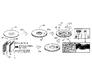
dispersibility of GO combined with inexpensive production methods make GO an
ideal starting material for producing carbon-based devices. In particular, GO
has
water dispersible properties. Unfortunately, the same oxygen species that give
GO its water dispersible properties also create defects in its electronic
structure,
and as a result, GO is an electrically insulating material. Therefore, the
development of device grade carbon-based films with superior electronic
properties requires the removal of these oxygen species, re-establishment of a
conjugated carbon network, as well as a method for controllably patterning
carbon-based device features.
[0008] Methods for reducing graphite oxide have included chemical
reduction
via hydrazine, hydrazine derivatives, or other reducing agents, high
temperature
annealing under chemical reducing gases and/or inert atmospheres,
solvothermal reduction, a combination of chemical and thermal reduction
methods, flash reduction, and most recently, laser reduction of GO. Although
several of these methods have demonstrated relatively high quality graphite
oxide reduction, many have been limited by expensive equipment, high
annealing temperatures and nitrogen impurities in the final product. As a
result,
of these difficulties, a combination of properties that includes high surface
area
and high electrical conductivity in an expanded interconnected carbon network
has remained elusive. In addition, large scale film patterning via an all-
encompassing step for both GO reduction and patterning has proven difficult
and
has typically been dependent on photo-masks to provide the most basic of
patterns. Therefore, what is needed is an inexpensive process for making and
patterning an interconnected corrugated carbon-based network (ICON) having a
high surface area with highly tunable electrical conductivity and
electrochemical
properties.
CA 02866250 2014-09-03
WO 2013/134207
PCT/US2013/029022
4
Summary
[0009] The present disclosure provides a capacitor having at least one
electrode made up of an interconnected corrugated carbon-based network
(ICCN). The ICCN produced has a combination of properties that includes high
surface area and high electrical conductivity in an expanded network of
interconnected carbon layers.
[0010] In one embodiment, each of the expanded and interconnected carbon
layers is made up of at least one corrugated carbon sheet that is one atom
thick.
In another embodiment, each of the expanded and interconnected carbon layers
is made up of a plurality of corrugated carbon sheets that are each one atom
thick. The interconnected corrugated carbon-based network is characterized by
a high surface area with highly tunable electrical conductivity and
electrochemical
properties.
[0011] In one embodiment, a method produces a capacitor having
electrodes
made of a patterned ICCN. In that particular embodiment, an initial step
receives
a substrate having a carbon-based oxide film. Once the substrate is received,
a
next step involves generating a light beam having a power density sufficient
to
reduce portions of the carbon-based oxide film to an ICCN. Another step
involves directing the light beam across the carbon-based oxide film in a
.. predetermined pattern via a computerized control system while adjusting the
power density of the light beam via the computerized control system according
to
predetermined power density data associated with the predetermined pattern.
[0012] In one embodiment, the substrate is a disc-shaped, digital
versatile
disc (DVD) sized thin plastic sheet removably adhered to a DVD sized plate
that
includes a DVD centering hole. The DVD sized plate carrying the disc-shaped
substrate is loadable into a direct-to-disc labeling enabled optical disc
drive. A
software program executed by the computerized control system reads data that
defines the predetermined pattern. The computerized control system directs a
laser beam generated by the optical disc drive onto the disc-shaped substrate,
thereby reducing portions of the carbon-based oxide film to an electrically
5
conductive ICCN that matches shapes, dimensions, and conductance levels
dictated by the data of the predetermined pattern.
[0012a] In accordance with another aspect, there is provided a capacitor
comprising: a first electrode; and a second electrode separated from the first
electrode by a dielectric wherein at least one of either the first electrode
or the
second electrode is made of an interconnected corrugated carbon-based network
(ICCN) having a plurality of expanded and interconnected carbon layers.
[0012b] In accordance with a further aspect, there is provided a capacitor
comprising: a first electrode made of an interconnected corrugated carbon-
based
network (ICCN) having a plurality of expanded and interconnected carbon
layers;
and a second electrode separated from the first electrode by a dielectric
wherein
at least one of either the first electrode or the second electrode is made of
ICCN
having a plurality of expanded and interconnected carbon layers.
[0012c] In accordance with another aspect, there is provided a capacitor
comprising: a first electrode; and a second electrode separated from the first
electrode by a dielectric wherein at least one of either the first electrode
or the
second electrode is made of an interconnected corrugated carbon-based network
(ICCN) having a plurality of expanded and interconnected carbon layers;
wherein the first electrode comprises a plurality of first extending electrode
digits
and the second electrode comprises a plurality of second extending electrode
digits that are interdigitated with the first extending electrode digits; and
wherein each of the plurality of first extending electrode digits and each of
the
plurality of second extending electrode digits are greater than about 330 pm
in
width.
[0012d] In accordance with a further aspect, there is provided a capacitor
comprising: a first electrode made of an interconnected corrugated carbon-
based
network (ICCN) having a plurality of expanded and interconnected carbon
layers;
and a second electrode separated from the first electrode by a dielectric
wherein
at least one of either the first electrode or the second electrode is made of
ICCN
having a plurality of expanded and interconnected carbon layers; wherein the
first
CA 2866250 2020-04-08
5a
electrode and the second electrode have line widths that approach a wavelength
of a light beam used to pattern the first electrode and the second electrode.
[0012e] In accordance with another aspect, there is provided a capacitor
comprising: a first electrode; and a second electrode separated from the first
electrode by a dielectric, wherein at least one of either the first electrode
or the
second electrode is made of an interconnected corrugated carbon-based network
(ICCN) having a plurality of expanded and interconnected carbon layers;
wherein
the first electrode comprises a plurality of first extending electrode digits
and the
second electrode comprises a plurality of second extending electrode digits
that
are interdigitated with the plurality of the first extending electrode digits;
and
wherein an interspace distance between each of the plurality of first
extending
electrode digits and each of the plurality of second extending electrode
digits is
less than about 150 pm.
[0012f] In accordance with a further aspect, there is provided a
capacitor
comprising: a first electrode; and a second electrode separated from the first
electrode by a dielectric, wherein at least one of either the first electrode
or the
second electrode is made of an interconnected corrugated carbon-based network
(ICCN) having a plurality of expanded and interconnected carbon layers;
wherein
theg first electrode comprises a plurality of first extending electrode digits
and the
second electrode comprises a plurality of second extending electrode digits
that
are interdigitated with the plurality of the first extending electrode digits;
and
wherein a total geometric area of the first electrode and the second electrode
is
less than about 50 mm2.
[0012g] In accordance with a further aspect, there is provided a capacitor
comprising: a first electrode; and a second electrode separated from the first
electrode by a dielectric, wherein at least one of either the first electrode
or the
second electrode is made of an interconnected corrugated carbon-based network
(ICCN) having a plurality of expanded and interconnected carbon layers;
wherein
the capacitor has a time constant of less than about 20 ms.
CA 2866250 2020-04-08
5b
[0012h] In accordance with a further aspect, there is provided a capacitor
comprising: a first electrode; and a second electrode separated from the first
electrode by a dielectric, wherein at least one of either the first electrode
or the
second electrode is made of an interconnected corrugated carbon-based network
(ICCN) having a plurality of expanded and interconnected carbon layers;
wherein
the plurality of expanded and interconnected carbon layers yields an
electrical
conductivity that is greater than about 1500 S/m.
[0012i] In accordance with a further aspect, there is provided a
capacitor
comprising: a first electrode; and a second electrode separated from the first
electrode by a dielectric, wherein at least one of either the first electrode
or the
second electrode is made of an interconnected corrugated carbon-based network
(ICCN) having a plurality of expanded and interconnected carbon layers;
wherein
the plurality of expanded and interconnected carbon layers has a surface area
that is greater than about 1000 square meters per gram (m2/g).
[0012j] In accordance with a further aspect, there is provided a capacitor
comprising: a first electrode; and a second electrode separated from the first
electrode by a dielectric, wherein at least one of either the first electrode
or the
second electrode is made of an interconnected corrugated carbon-based network
(ICCN) having a plurality of expanded and interconnected carbon layers;
wherein
a range of thicknesses of the plurality of expanded and interconnected carbon
layers is from about 7 pm to about 8 pm.
[0012k] In accordance with a further aspect, there is provided a capacitor
comprising: a first electrode; and a second electrode separated from the first
electrode by a dielectric, wherein at least one of either the first electrode
or the
second electrode is made of an interconnected corrugated carbon-based network
(ICCN) having a plurality of expanded and interconnected carbon layers;
wherein
an oxygen content of the expanded and interconnected carbon layers ranges
from about 1% to about 5%.
[00121] In accordance with a further aspect, there is provided a
capacitor
comprising: a first electrode; and a second electrode separated from the first
electrode by a dielectric, wherein at least one of either the first electrode
or the
CA 2866250 2020-04-08
5c
second electrode is made of an interconnected corrugated carbon-based network
(ICCN) having a plurality of expanded and interconnected carbon layers;
wherein
the plurality of expanded and interconnected carbon layers has a C/O ratio
that
ranges from about 333:1 to about 25:1.
[0012m] In accordance with a further aspect, there is provided a capacitor
comprising: a first electrode; and a second electrode separated from the first
electrode by a dielectric, wherein at least one of either the first electrode
or the
second electrode is made of an interconnected corrugated carbon-based network
(ICCN) having a plurality of expanded and interconnected carbon layers;
wherein
the plurality of expanded and interconnected carbon layers has a C/O ratio
that
ranges from about 333:1 to about 25:1.
[0012n] In accordance with a further aspect, there is provided a capacitor
comprising: a first electrode; and a second electrode separated from the first
electrode by a dielectric, wherein at least one of either the first electrode
or the
second electrode is made of an interconnected corrugated carbon-based network
(ICCN) having a plurality of expanded and interconnected carbon layers;
wherein
the plurality of expanded and interconnected carbon layers has a range of
Raman spectroscopy S3 second order peaks that ranges from about 2920 cm-1
to about 2930 cm-1.
[00120] In accordance with a further aspect, there is provided a capacitor
comprising: a first electrode; and a second electrode separated from the first
electrode by a dielectric, wherein at least one of either the first electrode
or the
second electrode is made of an interconnected corrugated carbon-based network
(ICCN) having a plurality of expanded and interconnected carbon layers;
wherein
a number of carbon layers in the plurality of expanded and interconnected
carbon
layers is greater than about 100.
[0013] Those skilled in the art will appreciate the scope of the
disclosure and
realize additional aspects thereof after reading the following detailed
description
in association with the accompanying drawings.
CA 2866250 2020-04-08
5d
Brief Description of the Drawings
[0014] The accompanying drawings incorporated in and forming a part of
this
specification illustrate several aspects of the disclosure, and together with
the
description serve to explain the principles of the disclosure.
[0015] Figure 1 depicts the label side of a prior art direct-to-disc
labeling type
CD/DVD disc.
[0016] Figure 2 is a schematic of a prior art direct-to-disc labeling
type optical
disc drive.
[0017] Figure 3 is a process diagram for an exemplary process for
providing
graphite oxide (GO) films on a substrate.
[0018] Figure 4 is a process diagram for laser scribing an
interconnected
corrugated carbon-based network (ICCN) and then fabricating electrical
components from the ICCN.
[0019] Figure 5 is a line drawing of a sample of the ICCN of the present
embodiments.
[0020] Figure 6A is an artwork image of a man's head covered with
circuits.
[0021] Figure 6B is a photograph of a GO film after the artwork image of
Figure 6A is directly patterned on the GO film using the laser scribing
technique
of the present disclosure.
[0022] Figure 7 is a graph that provides a comparison between changes in
electrical conductivity by reducing the GO film of Figure 6B by using various
grayscale levels to laser scribe the artwork of Figure 6A to produce the
patterned
GO film of Figure 6B.
CA 2866250 2020-04-08
CA 02866250 2014-09-03
WO 2013/134207
PCMJS2013/029022
6
[0023] Figure 8A is a scanning electron microscope (SEM) image that
illustrates an infrared laser's effect on GO film prior to laser treatment on
the right
side of the image in contrast to an aligned ICCN on the left side of the
image.
[0024] Figure 8B is an SEM image showing that an ICCN has a thickness
that
.. is approximately 10 times larger in comparison to that of untreated GO
film.
[0025] Figure 8C is an SEM image showing a cross-sectional view of a
single
laser converted ICCN.
[0026] Figure 8D is an SEM image showing a greater magnification of a
selected area within the ICCN in Figure 80.
[0027] Figure 9 compares a powder X-ray diffraction (XRD) pattern of the
ICCN with both graphite and graphite oxide diffraction patterns.
[0028] Figure 10 is a plot of log10 of peak current versus log10 of an
applied
voltammetric scan rate.
[0029] Figures 11A-11E are graphs related to Raman spectroscopy
analysis.
[0030] Figure 12A is a graph depicting an electrical resistance change of a
flexible ICCN electrode as a function of a bending radius.
[0031] Figure 12B is a graph depicting an electrical resistance change
of a
flexible ICCN electrode as a function of bending cycles.
[0032] Figure 13A is a cyclic voltammetry graph comparing a GO
electrochemical capacitor (EC) with an ICCN EC.
[0033] Figure 13B is a graph depicting galvanostatic charge/discharge
(CC)
curves of an ICCN EC measured at a high current density of 10 A/gi CCN/el ect
rode.
[0034] Figure 13C is a graph of volumetric stack capacitance of an ICCN
EC
that is calculated from the CC curves at different charge/discharge current
densities.
[0035] Figure 13D is a graph of ICCN EC cyclic stability versus CC
cycles.
[0036] Figure 13E is a graph of a complex plane plot of the impedance of
an
ICCN EC, with a magnification for the high-frequency region in a graph inset.
[0037] Figure 13F is a graph of impedance phase angle versus frequency
for
an ICCN EC and a commercial activated carbon EC.
[0038] Figure 14A is a structural diagram of an assembled ICCN EC.
CA 02866250 2014-09-03
WO 2013/134207
PCMJS2013/029022
7
[0039] Figure 14B is a graph of stack capacitance as a function of
current
density.
[0040] Figure 140 is a graph of capacitance retention for the ICCN EC
over a
4 month period.
[0041] Figure 14D is a graph of cyclic voltammetry (CV) performance of the
ICCN EC when tested under different bending conditions.
[0042] Figure 14E is a graph of galvanostatic charge/discharge curves
for four
tandem ICCN ECs connected in series.
[0043] Figure 14F is a graph of galvanostatic charge/discharge curves
for four
ICCN ECs in a series and parallel combination.
[0044] Figure 15 is a graph of galvanostatic charge/discharge curves of
the
device when operated at an ultrahigh current density of 250 A/gICCNielectrode=
[0045] Figure 16 is a Ragone plot comparing the performance of ICCN ECs
with different energy storage devices designed for high power
microelectronics.
[0046] Figure 17A is a structural diagram showing a set of interdigitated
electrodes made of ICCNs with dimensions of 6 mm x 6 mm, spaced at around
about 500 m, that are directly patterned onto a thin film of GO.
[0047] Figure 17B is a structural diagram showing the set of
interdigitated
electrodes transferred onto another type of substrate.
[0048] Figure 18A shows an exploded view of a micro-supercapacitor made
up of a plurality of expanded and interconnected carbon layers that are
electrically conductive.
[0049] Figure 18B shows the micro-supercapacitor of Figure 18A after
assembly.
[0050] Figure 19A depicts a micro-supercapacitor configuration having a
first
electrode with two extending electrode digits that are interdigitated with two
extending electrode digits of a second electrode.
[0051] Figure 19B depicts a micro-supercapacitor configuration having a
first
electrode with four extending electrode digits that are interdigitated with
four
extending electrode digits of a second electrode.
CA 02866250 2014-09-03
WO 2013/134207
PCMJS2013/029022
8
[0052] Figure 19C depicts a micro-supercapacitor configuration having a
first
electrode with eight extending electrode digits that are interdigitated with
eight
extending electrode digits of a second electrode.
[0053] Figure 20 is a table listing dimensions for the micro-
supercapacitors of
Figures 19A-190.
[0054] Figures 21A-21E depict the fabrication of ICCN micro-
supercapacitors.
[0055] Figure 22A depicts ICCN micro-devices with 4, 8, and 16
interdigitated
electrodes.
[0056] Figure 22B depicts an ICCN micro-device with 16 interdigitated
fingers
with 150-pm spacings.
[0057] Figure 220 is a tilted view (45 ) SEM image that shows the direct
reduction and expansion of the GO film after exposure to the laser beam.
[0058] Figures 22D and 22E show I-V curves of GO and an ICCN,
respectively.
[0059] Figure 22F is a graphical comparison of electrical conductivity
values
for GO and an ICCN.
[0060] Figures 23A-23I are graphs depicting electrochemical performance
of
ICCN micro-supercapacitors in PVA-H2SO4 gelled electrolyte.
[0061] Figures 24A-24F are graphs depicting the behavior of ICCN micro-
supercapacitors under mechanical stress in series and parallel configurations.
[0062] Figures 25A-25E are images depicting the fabrication of ICCN
micro-
supercapacitors on a chip along with graphs showing the characteristics of the
micro-supercapacitors.
[0063] Figures 26A-26B are graphs depicting self discharge rates for
ICON
micro-supercapacitors.
[0064] Figure 27 is a Ragone plot of energy and power densities of ICCN
micro-supercapacitors compared with commercially available energy storage
systems.
CA 02866250 2014-09-03
WO 2013/134207
PCT/US2013/029022
9
Detailed Description
[0065] The embodiments set forth below represent the necessary
information
to enable those skilled in the art to practice the disclosure and illustrate
the best
mode of practicing the disclosure. Upon reading the following description in
light
of the accompanying drawings, those skilled in the art will understand the
concepts of the disclosure and will recognize applications of these concepts
not
particularly addressed herein. It should be understood that these concepts and
applications fall within the scope of the disclosure and the accompanying
claims.
[0066] The present disclosure provides an inexpensive process for making
and patterning an ICCN having stringent requirements for a high surface area
with highly tunable electrical conductivity and electrochemical properties.
The
embodiments described herein not only meet these stringent requirements, but
provide direct control over the conductivity and patterning of an ICCN while
creating flexible electronic devices in a single step process. Moreover, the
.. production of the ICCN does not require reducing agents, or expensive
equipment. The simple direct fabrication of an ICCN on flexible substrates
therefore simplifies the development of lightweight electrical energy storage
devices. The ICCN can be synthesized on various substrates, such as plastic,
metal, and glass. Herein an electrochemical capacitor (EC), and in particular
a
micro-supercapacitor, is disclosed.
[0067] In at least one embodiment, the ICCNs are conducting films
produced
using a common and inexpensive infrared laser that fits inside a compact
disc/digital versatile disc (CD/DVD) optical drive unit that provides a direct-
to-disc
label writing function. LightScribe (Registered Trademark of Hewlett Packard
Corporation) and LabelFlash (Registered Trademark of Yamaha Corporation) are
exemplary direct-to-disc labeling technologies that pattern text and graphics
onto
the surface of a CD/DVD disc. LightScribe DVD drives are commercially
available for around $20 and the LightScribing process is controlled using a
standard desktop computer.
[0068] Figure 1 depicts the label side of a standard direct-to-disc
labeling type
CD/DVD disc 10 that includes a label area 12 and a clamping area 14 that
CA 02866250 2014-09-03
WO 2013/134207
PCMJS2013/029022
surrounds a centering hole 16. A dye film 18 covers the label area 12 and is
sensitive to laser energy that is typically directed onto the label area 12 to
produce a permanent visible image that may comprise graphics 20 and text 22.
A position tracking indicia 24 is usable by an optical disc drive (not shown)
to
5 accurately locate an absolute angular position of the CD/DVD disc 10
within the
optical disc drive so that the graphics 20 and/or text 22 can be re-written to
provide increased contrast. Moreover, the position tracking indicia 24 is
usable
by the optical disc drive to allow additional graphics and/or text to be
written
without undesirably overwriting the graphics 20 and/or text 22.
10 [0069] Figure 2 is a schematic of a prior art direct-to-disc
labeling type optical
disc drive system 26. In this exemplary case, the CD/DVD disc 10 is depicted
in
cross-section and loaded onto a spindle assembly 28 that is driven by a CD/DVD
spindle motor 30. The label area 12 is shown facing a laser assembly 32 that
includes a label writer laser (LWL) 34, a lens 36, and a focus actuator 38.
The
LWL 34 is typically a laser diode. Exemplary specifications for the LWL 34
includes a maximum pulse optical power of 350 mW at 780 nm emission and a
maximum pulse output power of 300 mW at 660 nm emission. A laser beam 40
emitted by the LWL 34 is focused by the lens 36 that is alternately translated
towards and away from the LWL 34 by the focus actuator 38 in order to maintain
focus of the laser beam 40 onto the label area 12 of the CD/DVD disc 10. The
laser beam 40 is typically focused to a diameter that ranges from around 0.7
p.m
to around 1 rim.
[0070] The laser assembly 32 is responsive to a control system 42 that
provides control signals 44 through an optical drive interface (ODI) 46. The
control system 42 further includes a central processor unit (CPU) 48 and a
memory 50. Label image data (LID) having information needed to realize a
permanent image to be written onto the label area 12 of the CD/DVD disc 10 is
processed by the CPU 48, which in turn provides an LID stream signal 52 that
pulses the LWL 34 on and off to heat the dye film 18 to realize the image
defined
.. by the LID.
CA 02866250 2014-09-03
WO 2013/134207
PCMJS2013/029022
11
[0071] The CPU 48 also processes the LID through the ODI 46 to provide a
position control signal 54 to a radial actuator 56 that translates the laser
assembly 32 in relation to the label area 12 in response to position
information
contained in the LID. In some versions of the present embodiments, the optical
disc drive system 26 monitors the focus of the laser beam 40 with an optical
receiver (not shown), so that the ODI 46 can generate a focus control signal
58
for the focus actuator 38. The ODI 46 also provides a motor control signal 60
for
the CD/DVD spindle motor 30 that maintains an appropriate rotation speed of
the
CD/DVD disc 10 while a label writing process is ongoing.
[0072] In some versions of the optical disc drive system 26 the LWL 34 is
used exclusively for label writing directly to the label area 12 of the CD/DVD
disc
10 and a separate laser diode (not shown) is used to write and/or read data
to/from a data side 62 of the CD/DVD disc 10. In other versions of the optical
disc drive system 26, the LWL 34 is used for label writing and data reading
and/or writing. When the LWL 34 is used for data reading and/or writing, the
CD/DVD disc 10 is flipped over to expose the data side 62 of the CD/DVD disc
10 to the laser beam 40. In versions wherein the LWL 34 is also used as a data
read/write laser, the laser assembly 32 includes optical pick-up components
(not
shown) such as a beam splitter and at least one optical receiver. The output
power of the LWL 34 is typically around 3 mW during data read operations.
[0073] In order to use the optical disc drive system 26 to realize an
inexpensive process for making and patterning an ICON having a high surface
area with highly tunable electrical conductivity and electrochemical
properties, a
carbon-based film is substituted for the dye film 18 (Figure 1). In one
embodiment, graphite oxide (GO) is synthesized from high purity graphite
powder using a modified Hummer's method. Dispersions of GO in water (3.7
mg/mL) are then used to make GO films on various substrates. Exemplary
substrates include but are not limited to polyethylene terephthalate (PET),
nitrocellulose membrane (with 0.4 pm pore size), aluminum foil, carbonized
aluminum, copper foil, and regular copier paper.
CA 02866250 2014-09-03
WO 2013/134207
PCT/US2013/029022
12
[0074] Referring to Figure 3, a process 100 begins with providing
graphite
powder 64. The graphite powder 64 undergoes an oxidation reaction using the
modified Hummer's method to become GO 66 (step 102). However, it is to be
understood that other oxidation methods for producing GO are available and
such methods are within the scope of the present disclosure. An exfoliation
procedure produces exfoliated GO 68 (step 104). The exfoliation procedure may
be accomplished via ultrasonication. It is to be understood that the
exfoliated GO
68 results from a partial exfoliation and not a complete exfoliation to a
single
layer of GO. The partial exfoliation is used to create a high accessible
surface
area that enables a fast redox response which enables a fast sensor response.
Additionally, the partial exfoliation of GO 68 provides the high surface area
for
growing metal nanoparticles that could then be used in catalysis. A substrate
70
carries a GO film 72 that is produced by a deposition procedure that deposits
the
exfoliated GO 68 onto the substrate 70 (step 106). In at least some
embodiments, a GO film 72 is made by either drop-casting or vacuum filtering
GO dispersions onto the substrate 70 that is the size of a CD/DVD disc. The GO
film 72 is typically allowed to dry for 24 hours under ambient conditions.
However, controlling conditions to expose the GO film 72 to a relatively lower
humidity and relatively higher temperature will dry the GO film 72 relatively
quickly. The term GO herein refers to graphite oxide.
[0075] Referring to Figure 4, individual ones of the GO film(s) 72 are
then
affixed to a substrate carrier 74, which has dimensions similar to the CD/DVD
disc 10 (Figure 1)(step 200). The substrate carrier 74 carrying the substrate
70
with the GO film 72 is loaded into the optical disc drive system 26 (Figure 2)
such
that the GO film 72 faces the LWL 34 for laser treatment (step 202). In this
way,
the present embodiments use the GO film 72 in place of the dye film 18 (Figure
1). It is to be understood that the substrate carrier 74 can be a rigid or
semi-rigid
disc onto which the GO film 72 can be fabricated directly. In that case, the
substrate carrier 74 replaces the function of the substrate 70.
[0076] Images 76 for realizing electrical components 78 are patterned in
concentric circles, moving outward from the center of the substrate carrier 74
CA 02866250 2014-09-03
WO 2013/134207
PCMJS2013/029022
13
(step 204). The laser irradiation process results in the removal of oxygen
species and the reestablishment of sp2carbons. This causes a change in the
conductivity of the GO film 72 with a typical resistance of >20 MO/sq to
become a
relatively highly conducting plurality of expanded and interconnected carbon
layers that make up an ICON 80. The number of times the GO film 72 is laser
treated results in a significant and controllable change in the conductivity
of the
ICCN 80. The ICON 80 has a combination of properties that includes high
surface area and high electrical conductivity in an expanded interconnected
network of carbon layers. In one embodiment, the plurality of expanded and
interconnected carbon layers has a surface area of greater than around about
1400 m2/g. In another embodiment, the plurality of expanded and interconnected
carbon layers has a surface area of greater than around about 1500 m2/g. In
yet
another embodiment, the surface area is around about 1520 m2/g. In one
embodiment, the plurality of expanded and interconnected carbon layers yields
an electrical conductivity that is greater than around about 1500 S/m. In
another
embodiment, the plurality of expanded and interconnected carbon layers yields
an electrical conductivity that is greater than around about 1600 S/m. In yet
another embodiment, the plurality of expanded and interconnected carbon layers
yields an electrical conductivity of around about 1650 S/m. In still another
embodiment, the plurality of expanded and interconnected carbon layers yields
an electrical conductivity that is greater than around about 1700 S/rn. In yet
one
more embodiment, the plurality of expanded and interconnected carbon layers
yields an electrical conductivity of around about 1738 S/m. Moreover, in one
embodiment, the plurality of expanded and interconnected carbon layers yields
an electrical conductivity that is greater than around about 1700 S/m and a
surface area that is greater than around about 1500 m2/g. In another
embodiment, the plurality of expanded and interconnected carbon layers yields
an electrical conductivity of around about 1650 S/m and a surface area of
around
about 1520 m2/g.
[0077] The electrical components 78 comprising electrodes 82 used in the
fabrication of an electrochemical capacitor (EC) 84 are laser irradiated 6
times
CA 02866250 2014-09-03
WO 2013/134207
PCMJS2013/029022
14
before reaching the relatively high conductivity of around about 1738 S/m. An
exemplary laser irradiation process takes around about 20 minutes per cycle.
However, it is to be understood that faster laser irradiation rates are
possible
depending on the power of the laser light emitted from the LWL 34 combined
with
an increased positioning rate of the substrate carrier. Moreover, other
imaging
techniques that employ photomasks and flashlamps may provide even faster
fabrication of the electrical components 78. Afterwards, the substrate 70
carrying
the ICCN 80 and any remaining GO film 72 is removed from the substrate carrier
74 (step 206). Next, the ICCN 80 is fabricated into the electrical components
78
that make up the EC 84 (step 208). In this exemplary case, portions of the
ICCN
80 on the substrate 70 are cut into rectangular sections to make the
electrical
components 78, which include the electrodes 82 formed from the ICCN 80. A
separator/electrolyte 86 is sandwiched between the electrodes 82 to form the
EC
84.
[0078] The ICCN 80 possesses a very low oxygen content of only around
about 3.5%, which contributes to a relatively very high charging rate. In
other
embodiments, the oxygen content of the expanded and interconnected carbon
layers ranges from around about 1% to around about 5%. Figure 5 is a line
drawing of a sample of the ICCN 80, which is made up of the plurality of
expanded and interconnected carbon layers that include corrugated carbon
layers such as a single corrugated carbon sheet 88. In one embodiment, each of
the expanded and interconnected carbon layers comprises at least one
corrugated carbon sheet that is one atom thick. In another embodiment, each of
the expanded and interconnected carbon layers comprises a plurality of
corrugated carbon sheets 88. The thickness of the ICCN 80, as measured from
cross-sectional scanning electron microscopy (SEM) and profilometry, was found
to be around about 7.6 pm. In one embodiment, a range of thicknesses of the
plurality of expanded and interconnected carbon layers making up the ICCN 80
is
from around about 7 tm to 8 pm.
[0079] As an illustration of the diversity in image patterning that is
possible, a
complex image formed by the direct laser reduction of GO is shown in Figures
6A
CA 02866250 2014-09-03
WO 2013/134207
PCMJS2013/029022
and 6B. Figure 6A is an artwork image of a man's head covered with circuits.
Figure 6B is a photograph of a GO film after the artwork image of Figure 6A is
directly patterned on the GO film using the laser scribing technique of the
present
disclosure. Essentially, any part of the GO film that comes in direct contact
with
5 the 780 nm infrared laser is effectively reduced to an ICCN, with the
amount of
reduction being controlled by the laser intensity; a factor that is determined
by
power density of the laser beam impinging on the GO film. The resulting image
of Figure 6B is an effective print of the original image of Figure 6A.
However, in
this case the image of Figure 6B is made up of various reductions of the GO
film.
10 As expected, the darkest black areas indicate exposure to the strongest
laser
intensities, while the lighter gray areas are only partially reduced. Since
different
grayscale levels directly correlate with the laser's intensity, it is possible
to tune
the electrical properties of the generated ICCN over five to seven orders of
magnitude in sheet resistance (Q/sq) by simply changing the grayscale level
15 used during the patterning process. As illustrated in Figure 7, there is
a clear
relationship between sheet resistance, grayscale level and the number of times
the GO film is laser irradiated. Control over conductivity from a completely
insulating GO film, with a typical sheet resistance value of >20 MO/sq, to a
conducting ICCN that registers a sheet resistance value of approximately 80
Q/sq, which translates to a conductivity of around about1650 S/m, is possible.
This method is sensitive enough to differentiate between similar grayscale
levels
as shown in the graph of Figure 7, where the sheet resistance varies
significantly
with only a small variation in grayscale level. In addition, the number of
times a
GO film is laser treated results in a significant and controllable change in
sheet
resistance. Each additional laser treatment lowers the sheet resistance as
seen
in Figure 7, where a film is laser irradiated once (black squares), twice
(circles)
and three times (triangles) with respect to the grayscale level. Therefore,
the
film's sheet resistance is tunable both by controlling the grayscale level
used and
the number of times the film is reduced by the laser, a property that has so
far
been difficult to control through other methods.
CA 02866250 2014-09-03
WO 2013/134207
PCMJS2013/029022
16
[0080] Scanning electron microscope (SEM) techniques are usable to
understand the effects a low energy infrared laser has on the structural
properties of GO film by comparing the morphological differences between an
ICCN and untreated graphite oxide GO film. Figure 8A is an SEM image that
illustrates the infrared laser's effect on GO film prior to laser treatment on
the
right side of the image in contrast to an aligned ICCN on the left side of the
image that occurs after being reduced with the infrared laser. The image not
only
gives a clear definition between the ICCN and untreated GO regions, but also
demonstrates the level of precision possible when using this method as a means
to pattern and reduce GO. The regions of ICCN, which result from the laser
treatment, can be further analyzed through cross-sectional SEM.
[0081] Figure 8B is an SEM image showing a cross-sectional view of a
free
standing film of laser treated and untreated GO film, which shows a
significant
difference between GO film thicknesses. As indicated by the white brackets in
Figure 8B, an ICCN increases in thickness by approximately 10 times in
comparison to that of untreated GO film. Moreover, a range of thicknesses of
the
plurality of expanded and interconnected carbon layers is from around about 7
pm to around 8 pm. In one embodiment, an average thickness of the plurality of
expanded and interconnected carbon layers is around about 7.6 pm. The
increased thickness stems from rapid degassing of gases generated and
released during laser treatment, similar to thermal shock, which effectively
causes the reduced GO to expand and exfoliate as these gases rapidly pass
through the GO film. Figure 8C is an SEM image showing a cross-sectional view
of a single ICCN, which shows an expanded structure that is a characteristic
of
the ICCN of the present disclosure.
[0082] Figure 8D is an SEM image showing a greater magnification of a
selected area within the ICCN in Figure 80. The SEM image of Figure 8D allows
the thickness of the plurality of expanded and interconnected carbon layers to
be
calculated to be between around about 5-10 nm. However, the number of
.. carbon layers in the plurality of expanded and interconnected carbon layers
making up the ICCN is greater than around about 100. In another embodiment
CA 02866250 2014-09-03
WO 2013/134207
PCMJS2013/029022
17
the number of carbon layers in the plurality of expanded and interconnected
carbon layers is greater than around about 1000. In yet another embodiment the
number of carbon layers in the plurality of expanded and interconnected carbon
layers is greater than around about 10,000. In still another embodiment, the
number of carbon layers in the plurality of expanded and interconnected carbon
layers is greater than around about 100,000. The SEM analysis shows that
although an infrared laser emission is only marginally absorbed by GO, enough
power and focus (i.e., power density) can cause sufficient thermal energy to
efficiently reduce, deoxygenate, expand, and exfoliate the GO film. Moreover,
the surface area of the ICON is greater than around about 1500 m2/g.
[0083] Since each of the carbon layers has a theoretical surface area of
around about 2630 m2/g, a surface greater than around about 1500 m2/g
indicates that almost all surfaces of the carbon layers are accessible. The
ICON
has an electrical conductivity that is greater than around about 17 S/cm. The
ICCN forms when some wavelength of light hits the surface of the GO, and is
then absorbed to practically immediately convert to heat, which liberates
carbon
dioxide (002). Exemplary light sources include but are not limited to a 780 nm
laser, a green laser, and a flash lamp. The light beam emission of the light
sources may range from near infrared to ultraviolet wavelengths. The typical
carbon content of the ICON is greater than around about 97% with less than
around about 3% oxygen remaining. Some samples of the ICON are greater
than around about 99% carbon even though the laser reduction process is
conducted in the air.
[0084] Figure 9 compares a powder X-ray diffraction (XRD) pattern of the
corrugated carbon-based network with both graphite and graphite oxide
diffraction patterns. A typical XRD pattern for graphite, shown in Figure 9
trace
A, displays the characteristic peak of 20= 27.8 with a d-spacing of 3.20 A.
An
XRD pattern (Figure 9, trace B) for GO, on the other hand, exhibits a single
peak
of 20. 10.76 , which corresponds to an interlayer d-spacing of 8.22 A. The
increased d-spacing in GO is due to the oxygen containing functional groups in
graphite oxide sheets, which tend to trap water molecules between the basal
CA 02866250 2014-09-03
WO 2013/134207
PCMJS2013/029022
18
planes, causing the sheets to expand and separate. The XRD pattern of the
corrugated carbon-based network (Figure 9, trace C) shows the presence of both
GO (10.76 20) and a broad graphitic peak at 25.97 20ass0ciated with a d-
spacing of 3.43 A. The GO presence in the corrugated carbon-based network is
expected since the laser has a desirable penetration depth, which results in
the
reduction of only the top portion of the film with the bottom layer being
unaffected
by the laser. The small presence of GO is more prominent in thicker films, but
begins to diminish in thinner films. In addition, one can also observe a
partially
obstructed peak at 26.66 20, which shows a similar intensity to the broad
25.97
20 peak. Both of these peaks are considered graphitic peaks, which are
associated to two different lattice spacing between basal planes.
[0085] It has been previously shown that the immobilization of carbon
nanotubes (CNTs) on glassy carbon electrodes will result in a thin CNT film,
which directly affects the voltammetric behavior of the CNT modified
electrodes.
In a ferrogerrocyanide redox couple, the voltammetric current measured at the
CNT modified electrode will likely have two types of contributions. The thin
layer
effect is a significant contributor to the voltammetric current. The thin
layer effect
stems from the oxidation of ferrocyanide ions, which are trapped between the
nanotubes. The other contribution results from the semi-infinite diffusion of
ferrocyanide towards the planar electrode surface. Unfortunately, the
mechanistic information is not easily de-convoluted and requires knowledge of
the film thickness.
[0086] In contrast, no thin layer effect is observed in association with
the
interconnected corrugated carbon-based network of the present disclosure.
Figure 10 is a plot of log10 of peak current versus log10 of an applied
voltammetric
scan rate. In this case, no thin layer effect is observed since the plot has a
consistent slope of 0.53 and is linear. The slope of 0.53 is relatively close
to
theoretical values calculated using a semi-infinite diffusion model governed
by
the Randles-Sevcik equation:
CA 02866250 2014-09-03
WO 2013/134207
PCMJS2013/029022
19
=0.3443A6 D0v(nF)3
RT
[0087] Raman spectroscopy is used to characterize and compare the
structural changes induced by laser treating GO film. Figures 11A-11E are
graphs related to Raman spectroscopic analysis. As can be seen in Figure 11A,
characteristic D, G, 20 and S3 peaks are observed in both GO and the ICCN.
The presence of the D band in both spectra suggests that carbon sp3 centers
still
exist after reduction. Interestingly, the spectrum of the ICCN shows a slight
increase in the D band peak at around about 1350 cm-1. This unexpected
increase is due to a larger presence of structural edge defects and indicates
an
overall increase in the amount of smaller graphite domains. The result is
consistent with SEM analysis, where the generation of exfoliated accordion-
like
graphitic regions (Figure 5) caused by the laser treatment creates a large
number
of edges. However the D band also shows a significant overall peak narrowing,
suggesting a decrease in these types of defects in the ICCN. The G band
experiences a narrowing and a decrease in peak intensity as well as a peak
shift
from around about 1585 to 1579 cm-1. These results are consistent with the re-
establishment of sp2 carbons and a decrease in structural defects within the
basal planes. The overall changes in the G band indicate a transition from an
amorphous carbon state to a more crystalline carbon state. In addition, a
prominent and shifted 2D peak from around about 2730 to around about 2688
cm1 is seen after GO is treated with the infrared laser, indicating a
considerable
reduction of the GO film and strongly points to the presence of a few-layer
interconnected graphite structure. In one embodiment, the 20 Raman peak for
the ICCN shifts from around about 2700 cm-1to around about 2600 cm-1 after the
ICCN is reduced from a carbon-based oxide. Moreover, as a result of lattice
disorder, the combination of D-G generates an S3 second order peak, which
appears at around about 2927 cm-1 and, as expected, diminishes with
decreasing disorder after infrared laser treatment. In some embodiments, the
plurality of expanded and interconnected carbon layers has a range of Raman
spectroscopy S3 second order peak that ranges from around about 2920 cm-1 to
CA 02866250 2014-09-03
WO 2013/134207
PCMJS2013/029022
around about 2930 cm-1. The Raman analysis demonstrates the effectiveness of
treating GO with an infrared laser as a means to effectively and controllably
produce the ICON.
[0088] X-ray photoelectron spectroscopy (XPS) was employed to correlate
the
5 effects of laser irradiation on the oxygen functionalities and to monitor
the
structural changes on the GO film. Comparing the carbon to oxygen (C/O) ratios
between GO and the ICON provides an effective measurement of the extent of
reduction achieved using a simple low energy infrared laser. Figure 11B
illustrates the significant disparity between the 0/0 ratios before and after
laser
10 .. treatment of the GO films. Prior to laser reduction, typical GO films
have a 0/0
ratio of approximately 2.6:1, corresponding to a carbon/oxygen content of
around
about 72% and 38%. In one exemplary embodiment, the ICON has an enhanced
carbon content of around about 96.5% and a diminished oxygen content of
around about 3.5%, giving an overall 0/0 ratio of 27.8:1. In yet another
15 exemplary embodiment, a laser reduction of GO results in a 0/0 ratio of
333:1,
which is around about 0.3% oxygen content. This relatively low oxygen content
was measured using photoelectron spectroscopy (XPS). In other embodiments,
the plurality of expanded and interconnected carbon layers has a C/O ratio
that
ranges from around about 333:1 to around about 25:1. Since the laser reduction
20 process takes place under ambient conditions, it is postulated that some
of the
oxygen present in the ICON film is a result of the film having a static
interaction
with oxygen found in the environment.
[0089] Figure 11C shows that the C1s XPS spectrum of GO displays two
broad peaks, which can be resolved into three different carbon components
corresponding to the functional groups typically found on the GO surface, in
addition to a small IF to Tr* peak at 290.4 eV. These functional groups
include
carboxyl, sp3carbons in the form of epoxide and hydroxyl, and sp2 carbons,
which are associated with the following binding energies: approximately 288.1,
286.8 and 284.6 eV, respectively.
[0090] Figure 11D shows expected results, in that the large degree of
oxidation in GO results in various oxygen components in the GO Cis XPS
CA 02866250 2014-09-03
WO 2013/134207
PCMJS2013/029022
21
spectrum. These results are in contrast to the ICCN, which shows a significant
decrease in oxygen containing functional groups and an overall increase in the
C-C sp2 carbon peak. This points to an efficient deoxygenating process as well
as the re-establishment of C=C bonds in the ICCN. These results are consistent
with the Raman analysis. Thus, an infrared laser such as the LWL 34 (Figure 2)
is powerful enough to remove a majority of the oxygen functional groups, as is
evident in the XPS spectrum of the ICCN, which only shows a small disorder
peak and a peak at 287.6 eV. The latter corresponds to the presence of sp3
type
carbons suggesting that a small amount of carboxyl groups remain in the final
product. In addition, the presence of a 7 to -rr* satellite peak at -290.7 eV
indicates that delocalized 7 conjugation is significantly stronger in the ICCN
as
this peak is miniscule in the GO XPS spectrum. The appearance of the
delocalized 7 peak is a clear indication that conjugation in the GO film is
restored
during the laser reduction process and adds support that an sp2 carbon network
has been re-established. The decreased intensity of the oxygen containing
functional groups, the dominating C=C bond peak and the presence of the
delocalized 7 conjugation all indicate that a low energy infrared laser is an
effective tool in the generation of the ICCN.
[0091] Figure 11E depicts UV-visible light absorbance spectra of GO
shown in
black. The inset shows a magnified view of the boxed area showing the
absorbance of GO with respect to a 780 nm infrared laser in the 650 to 850 nm
region.
[0092] Having established that an ICCN has an effective 7 conjugation,
it is
possible to construct devices to make use of the conducting material. In this
regard, at least one embodiment of the present disclosure provides the
production of ICCN ECs through a simple all-solid-state approach that avoids
the
restacking of carbon sheets such as the corrugated carbon sheet 88 (Figure 5).
Irradiation of the GO film 72 (Figure 3) with an infrared laser such as the
LWL 34
(Figure 2) inside the inexpensive commercially available direct-to-disc
labeling
type optical disc drive system 26 (Figure 2) which, as discussed above,
reduces
the GO film 72 to an ICCN, as indicated by the change in film color from
golden
CA 02866250 2014-09-03
WO 2013/134207
PCMJS2013/029022
22
brown to black. Analysis of cross sections of the film with scanning electron
microscopy showed that the initially stacked GO sheets were converted into
partially-exfoliated carbon sheets through laser irradiation (Figure 3). The
resulting ICCN showed excellent conductivity (around about 1738 S/m) as
opposed to 10 to 100 S/m for activated carbons, the current state-of-the-art
material used in commercial devices.
[0093] In addition, Figures 12A and 12B show that the ICCN made up of
corrugated carbon sheets shows excellent mechanical flexibility with only
around
about 1% change in the electrical resistance of the film after 1000 bending
cycles. Thus, ICCNs can be directly used as EC electrodes without the need for
any additional binders or conductive additives. More importantly, these
properties allow ICCNs to act as both an active material and current collector
in
the EC. The combination of both functions in a single layer leads to a
simplified
and lightweight architecture. Thus, a device can be readily made by
sandwiching
an ion porous separator [Celgard 3501 (Celgard, Charlotte, NC)] between two
ICCN electrodes. ICCN ECs are relatively thin with a total thickness of less
than
around about 100 mm, making them potentially useful in microdevice
applications. Other devices can be made by putting ICCNs on porous substrates
such as a nitrocellulose membrane or photocopy paper or on conductive
aluminum foil, which is often used in commercial devices. Therefore, ICCN ECs
can be readily made into different designs, including stacked and spirally
wound
structures to target different applications.
[0094] The ICCN electrodes are fabricated to satisfy the critical
features for
high-performance ECs. First, the relatively large and accessible specific
surface
area of an ICCN (1520 m2/g compared with 1000 to 2000 m2/g for a typical
activated carbon material) results in a sizeable charge storage capacity and
accounts for the high areal and volumetric stack capacitances observed.
Second, the LWL 34 (Figure 2) that is typically a LightScribe or a LabelFlash
laser, causes the simultaneous reduction and partial exfoliation of GO sheets
and
produces the ICCN 80 (Figure 5). The novel structure of the ICCN 80 is porous,
which prevents the agglomeration of carbon sheets, which has been a major
CA 02866250 2014-09-03
WO 2013/134207
PCMJS2013/029022
23
barrier in achieving the full potential of carbon-based ECs. The network
structure
of the ICCN 80 has open pores, which facilitates electrolyte accessibility to
the
electrode surfaces. This offers an opportunity to optimize ionic diffusion in
the
electrodes 82, which is crucial for charging the electrochemical double layers
(EDLs), and generates high power ECs. Moreover, the ICCN 80 possesses
excellent electronic conductivity, which is another key factor for achieving
high
power. Working with these properties, three dimensional composite electrodes
have been successfully used to make batteries with relatively high energy
density
and fast charge/discharge rates. Although activated carbons can provide high
surface area, the difficulty of controlling their pore structure and pore size
distribution has so far limited the energy densities and rate capabilities of
commercial ECs.
[0095] In order to demonstrate the superior performance of ICCN
electrodes
for electrochemical energy storage, symmetric ICON ECs were assembled using
polyethylene terephthalate (PET) as a thin flexible substrate and an aqueous
electrolyte of 1.0 molar (M) phosphoric acid (H3PO4). As shown in Figures 13A-
13F, the ICCN EC performance was analyzed through both cyclic voltammetry
(CV) and galvanostatic charge/discharge (CC) experiments. In comparison with
GO, the ICCN EC shows an enhanced electrochemical performance with a
nearly rectangular CV shape at a scan rate of 1000 mV/s, which is indicative
of
nearly ideal capacitive behavior (Figure 13A) even though no metal current
collectors, binders, or electroactive additives were used, as is the case in
commercial ECs. Additionally, the ICCN EC is robust enough to be charged and
discharged over a wide range of scan rates (100 to 10,000 mV/s) and still
maintain its nearly ideal rectangular CV shape. Figure 13B shows the nearly
triangular shape of the CC curves obtained at a high current density of 10 A/g
of
ICCN per electrode (abbreviated 10 A/gICCN/electrode)= This is indicative of
the
formation of an efficient EDL and fast ion transport within the ICCN
electrodes.
In addition, these CC curves show only a small voltage drop of 0.018 V at the
start of the discharge curve, indicating a device with a low equivalent series
resistance (ESR). The specific capacitance from the CC curves was measured
CA 02866250 2014-09-03
WO 2013/134207
PCMJS2013/029022
24
over a wide range of charge/discharge current densities. Here, the areal and
volumetric capacitances of the stack (this includes the flexible substrate,
the
current collector, the active material, and the separator) were calculated and
compared with a commercial activated-carbon EC (AC-EC) tested under the
same dynamic conditions. Although the AC-EC shows a slightly higher
volumetric capacitance at low charge/discharge rates, its capacitance falls
off
quickly at higher rates, whereas the ICCN EC continues to provide high
capacitance even when operated at very high rates (Figure 130). In addition,
the
areal capacitance of the ICCN EC was calculated to be 3.67 mF/cm2 and
4.04mF/cm2 in 1.0 M H2SO4 at 1 A/gICCNIelectrode= The device also shows a very
high rate capability while still maintaining a capacitance of more than 1.84
mF/cm2, even when the ICCN EC is operated at an ultrafast charge/discharge
rate of 1000 A/g ICCN/electrode= This is comparable with values reported in
the
literature for micro-devices and thin film ECs at much lower current
charge/discharge rates (0.4 to 2 mF/cm2). These ECs can be efficiently
charged/discharged on the 0.1-s time scale. Additionally, the ICCN EC retained
around about 96.5% of its initial capacitance after 10,000 cycles (Figure
13D).
[0096] Electrochemical impedance spectroscopy (EIS) confirmed fast ion
transport within the ICCN electrodes. A complex plan plot of the impedance
data
of the ICCN EC is shown in Figure 13E with an expanded view provided in the
inset. The device displays a pure capacitive behavior, even at high
frequencies
of up to -158 Hz. The series resistance of the device is estimated to be -16
ohms. This value can be attributed to the contact resistance of the device
with
the external circuit that could be reduced by using current collectors. The
dependence of the phase angle on the frequency for the ICCN EC, AC-EC, and
an aluminum electrolytic capacitor is shown in Figure 13F. For frequencies up
to
10 Hz, the phase angle of the ICCN EC is close to -90 , which suggests that
the
device functionality is close to that of an ideal capacitor. The
characteristic
frequency f0 for a phase angle of -45 is 30 Hz for the ICCN EC. This
frequency
marks the point at which the resistive and capacitive impedances are equal.
The
corresponding time constant tO (.1/f0) equals 33 ms compared with 10 seconds
CA 02866250 2014-09-03
WO 2013/134207
PCMJS2013/029022
for the conventional AC-EC and 1 ms for the aluminum electrolytic capacitor.
This rapid frequency response of the ICON EC can be accounted for by the large
and accessible surface area of the ICON, whose exposed flat sheets enhance
the ion transport rate in the device. This is consistent with results reported
5 recently for an EC made from vertically oriented graphene nanosheets
grown
directly on metal current collectors and carbon nanotube electrodes made with
an electrophoretic deposition technique.
[0097] The future development of multifunctional flexible electronics
such as
roll-up displays, photovoltaic cells, and even wearable devices presents new
10 challenges for designing and fabricating lightweight, flexible energy
storage
devices. Commercially available ECs consist of a separator sandwiched
between two electrodes with liquid electrolyte, which is then either spirally
wound
and packaged into a cylindrical container or stacked into a button cell.
Unfortunately, these device architectures not only suffer from the possible
15 harmful leakage of electrolytes, but their design makes it difficult to
use them for
practical flexible electronics. Referring to Figure 14A depicting the
structure of
the EC 84, the liquid electrolyte was replaced with poly(vinyl alcohol) (PVA)-
H3PO4 polymer gelled electrolyte, which also acts as the separator. This
electrolyte reduced the device thickness and weight compared with phosphoric
20 acid and simplified the fabrication process because it does not require
any
special packaging materials. As demonstrated in Figure 14B, at any given
charge/discharge rate, the specific capacitance values for the all-solid-state
device were comparable with those obtained with an aqueous electrolyte. The
high-rate performance of the EC 84 can be accounted for by the porous
structure
25 of the ICON electrodes, which can effectively absorb the gelled
electrolyte and
act as an electrolyte reservoir to facilitate ion transport and minimize the
diffusion
distance to the interior surfaces. Another key factor is that ICON electrodes
are
binder free, thus enabling a reduction in interfacial resistance and enhancing
the
electrochemical reaction rate. As illustrated in Figure 14C, the device
performance was completely stable over 4 months of testing. As with the
aqueous ICON EC, the flexible all-solid-state ICCN EC maintains its excellent
CA 02866250 2014-09-03
WO 2013/134207
PCT/US2013/029022
26
cycling stability: >97% of the initial capacitance was maintained even after
10,000 cycles.
[0098] In order to evaluate under real conditions the potential of all-
solid-state
ICCN ECs, such as the EC 84, for flexible energy storage, a device was placed
under constant mechanical stress and its performance analyzed. Figure 14D
shows the CV performance of this device when tested under different bending
conditions. The bending had almost no effect on the capacitive behavior; it
can
be bent arbitrarily without degrading performance. Moreover, the stability of
the
device was tested for more than 1000 cycles while in the bent state, with only
-5% change in the device capacitance. This performance durability can be
attributed to the high mechanical flexibility of the electrodes along with the
interpenetrating network structure between the ICCN electrodes and the gelled
electrolyte. The electrolyte solidifies during the device assembly and acts
like a
glue that holds all the device components together, improving the mechanical
integrity and increasing its cycle life even when tested under extreme bending
conditions. Because the increased cycle life of the present EC has yet to be
realized in commercial devices, the present ECs may be ideal for next-
generation
flexible, portable electronics.
[0099] Portable equipment often requires cells packaged either in
series, in
parallel, or in combinations of the two in order to meet energy and power
requirements. For example, laptop batteries commonly have four 3.6-V lithium
ion cells connected in series to achieve a voltage of 14.4 V, and two in
parallel to
increase the capacity from 2400 mAh to 4800 mAh. Thus, it would be of interest
to develop an EC that could exhibit control over the operating voltage and
current
by using tandem serial and parallel assemblies with minimal energy losses. The
performances of a set of tandem ICCN ECs were evaluated by assembling four
devices both in series and in parallel configurations. Compared with a single
EC,
which operates at 1.0 V, the tandem series ECs exhibited a 4.0 V
charge/discharge voltage window. In the parallel assembly, the output current
.. increased by a factor of 4, and thus the discharge time was four times that
of a
single device when operated at the same current density. As expected, when the
CA 02866250 2014-09-03
WO 2013/134207
PCMJS2013/029022
27
four ECs were combined, two in series and two in parallel, both the output
voltage and the runtime (capacitive current) increased by a factor of 2 under
the
same charge/discharge current. As with the single devices, the tandem devices
show essentially perfect triangular CC curves with a miniscule voltage drop,
which again indicates excellent capacitive properties with minimal internal
resistance. Thus, when used in tandem, the ICCN ECs undergo minimal energy
losses. As a demonstration, a tandem EC's ability to light a red light-
emitting
diode (LED) that operates at a minimum voltage of 2 V is shown in the Figures
14E and 14F.
.. [00100] An organic electrolyte was also examined, and was discovered to
allow
the operation of the devices at higher voltages, thus achieving higher energy
densities. In this case, tetraethylammonium tetrafluoroborate dissolved in
acetonitrile was used because this is the most common organic electrolyte used
in commercial devices. As shown in Figure 15, the ICCN EC again exhibits
enhanced performance and rate capabilities when compared with the commercial
AC-EC; this is consistent with the data acquired in the aqueous and gelled
electrolytes. Furthermore, the ICCN EC can be operated over a wider voltage
window of 3 V. This ICCN EC offers a specific capacitance of up to 4.82 mF/cm2
(265 F/gICCNieleclrode) and retains a capacitance of 2.07 mF/cm2 when operated
at
the ultrahigh current density of 1000 A/gICCN/electrode= Recently, room-
temperature
ionic liquids have been intensively studied as an attractive alternative to
conventional electrolytes for ECs because of their high ion density, good
thermal
stability, and nonvolatility, as well as their wider potential window when
compared
with organic electrolytes. An ICCN EC was fabricated using the ionic liquid 1-
.. ethyl-3-methylimidazoliumtetrafluoroborate (EMIMBF4) that exhibited a
specific
capacitance as high as 5.02 mF/cm2 (276 F/gICCN/electrode) and at a wider
potential
window of 4 V. A prototype ICCN EC was made and encapsulated in the
EMIMBF4 electrolyte, charged at a constant potential of 3.5 V, and used to
energize a red LED for -24 minutes.
[00101] Figure 16 is a Ragone plot comparing the performance of ICCN ECs
with different energy storage devices designed for high power
microelectronics.
CA 02866250 2014-09-03
WO 2013/134207
PCMJS2013/029022
28
Figure 16 also shows the overall performance of the ICON ECs using various
electrolytes. The Ragone plot includes a commercial 2.75 V/44 mF AC-EC and a
4 V/500- Ah thin film lithium battery and a 3 V/300 F aluminum electrolytic
capacitor, all tested under the same dynamic conditions. The plot shows the
volumetric energy density and power density of the stack for all the devices
tested. The ICON EC can exhibit energy densities of up to 1.36 mWh/cm3, which
is a value that is approximately two times higher than that of the AC-EC.
Additionally, ICON ECs can deliver a power density of around about 20 W/cm3,
which is 20 times higher than that of the AC-EC and three orders of magnitude
higher than that of the 4 V/500-1..tAh thin film lithium battery. Although the
electrolytic capacitor delivers ultrahigh power, it has an energy density that
is
three orders of magnitude lower than the ICON EC. Because of the simplicity of
the device architecture and the availability of the GO precursor which is
already
manufactured on the ton scale, the ICCN ECs of the present embodiments hold
promise for commercial applications.
[00102] Embodiments of the present disclosure also include other types of
ECs, such as planer and interdigitated ECs. For example, Figure 17A shows a
set of interdigitated electrodes with dimensions of 6 mm x 6 mm, spaced at
around about 500 um, that are directly patterned onto a thin film of GO. Prior
to
being patterned, the GO film was deposited on a thin flexible substrate,
polyethylene terephthalate (PET), in order to fabricate a set of electrodes
that are
mechanically flexible. The top arrow points to the region of the ICON that
makes
up the black interdigitated electrodes, while the bottom arrow points to the
un-
reduced GO film. Since the electrodes are directly patterned onto the GO film
on
a flexible substrate, the need for post-processing such as transferring the
film to
a new substrate is unnecessary. Although, if desired, a peel and stick method
could be used to selectively lift-off the black interdigitated electrodes made
of
ICON(s) with e.g. polydimethysiloxane (PDMS) and transfer it onto other types
of
substrates (Figure 17B). The simplicity of this method allows substantial
control
over pattern dimensions, substrate selectivity and electrical properties of
the
CA 02866250 2014-09-03
WO 2013/134207
PCMJS2013/029022
29
ICCN(s) by controlling laser intensity and thereby the amount of reduction in
each film.
[00103] These interdigitated electrodes can, in turn, be used to construct
supercapacitors. Figure 18A shows an exploded view of a micro-supercapacitor
90 having a first electrode 92 and a second electrode 94 that are fabricated
from
ICCNs made up of a plurality of expanded and interconnected carbon layers that
are electrically conductive. It is to be understood that optionally either the
first
electrode 92 or the second electrode 94 can be made of a metal, while the
remaining one of either the first electrode 92 or the second electrode 94 is
made
of ICCNs. However, the first electrode 92 and the second electrode 94 are
typically laser scribed from a GO film disposed onto a suitable substrate 96
such
as PET or silicon (Si) having an insulating layer 97 such as a silicon dioxide
(5i02) layer. A first conductive strip 98 and a second conductive strip 100
are
interfaced with the first electrode 92 and the second electrode 94 to provide
electrically conductive terminals to couple to external circuitry (not shown).
Exemplary external circuitry to be powered by the micro-supercapacitor 90 can
be, but is not limited to, integrated circuits and other electrically powered
micro-
scale devices. A liner 102 that is non-electrically conductive covers the
portions
of the first electrode 92 and the second electrode 94 that are interfaced with
the
first conductive strip 98 and the second conductive strip 100. The liner 102
includes a central window through which an electrolyte 104 is placed in
contact
with the first electrode 92 and the second electrode 94. A polyimide tape can
be
used as the liner 102. The electrolyte is preferably a gel electrolyte such as
fumed silica (FS) nano-powder mixed with an ionic liquid. An exemplary ionic
liquid is 1-buty1-3-methylimidazolium bis(trifluoromethylsulfonyl)imide.
Another
suitable gel electrolyte is a hydrogel such as poly(vinyl alchohol) (PVA)-
H2504.
Other electrolytes are also suitable, but the disclosed electrolytes provide a
voltage window between a maximum charged voltage and a minimum
discharged voltage of around about 2.5V.
[00104] Figure 18B depicts the micro-supercapacitor 90 fully assembled. In
this exemplary depiction, the first conductive strip 98 becomes a positive
terminal
CA 02866250 2014-09-03
WO 2013/134207
PCMJS2013/029022
and the second conductive strip 100 becomes a negative terminal. It is to be
understood that the first conductive strip 98 and the second conductive strip
100
may be made from an electrical conductor such as copper (Cu), aluminum (Al),
and/or additional ICON structures.
5 [00105] Figure 19A depicts a micro-supercapacitor configuration having a
first
electrode 106 with two extending electrode digits 108A and 108B. A second
electrode 110 has two extending electrode digits 112A and 112B that are
interdigitated with the extending electrodes digits 108A and 108B.
[00106] Figure 19B depicts another micro-supercapacitor configuration having
10 a first electrode 114 with four extending electrode digits 116A through
116D. A
second electrode 118 has four extending electrode digits 120A through 1200
that
are interdigitated with the four extending electrodes digits 116A through
116D.
[00107] Figure 190 depicts yet another micro-supercapacitor configuration
having a first electrode 122 with eight extending electrode digits 124A
through
15 124H. A second electrode 126 has eight extending electrode digits 128A
through
128H that are interdigitated with the eight extending electrode digits 124A
through 124H.
[00108] Figure 20 is a table listing exemplary dimensions for the micro-
supercapacitors of Figures 19A-19C. Referring to both Figure 20 and Figure
20 19A, the extending electrode digits 108A, 108B, 112A, and 112B are
depicted
with exemplary individual widths (W) of 1770 pm. The extending electrode
digits
108A, 108B, 112A, and 112B are depicted with an exemplary length (L) of 4800
pm.
[00109] Referring to both Figure 19B and Figure 20, the width of the extending
25 electrode digits 116A through 116D and the extending electrode digits
120A
through 120D are depicted with exemplary individual widths of 810 pm.
Referring to both Figure 190 and Figure 20, the extending electrode digits
124A
through 124H and the extending electrode digits 128A through 128H are
depicted with exemplary individual widths of 330 pm. The exemplary
30 configurations shown in Figures 19A, 19B, and 19C all have an exemplary
edge
dimension (E) of 200 pm, and an exemplary interspace dimension (I) that
CA 02866250 2014-09-03
WO 2013/134207
PCMJS2013/029022
31
separates the first electrodes 106, 114, and 122 from the second electrodes
110,
118, and 126 with a serpentine gap. Moreover, the exemplary micro-
supercapacitor configurations shown in Figures 19A, 19B, and 190 each have a
total area 40 mm2. In regard to the micro-supercapacitor configurations of
Figures 19A, 19B, and 190, it is to be understood that ranges of widths (W)
are
available for each of the first extending electrode digits 108A, 108B, 116A
through 116D, and 124A through 124H and each of the second extending
electrode digits 112A, 112B, 120A through 120D, and 128A through 128H. In
various exemplary embodiments, the width (W) of each of the first extending
.. electrode digits 108A, 108B, 116A through 116D, and 124A through 124H and
for each of the second extending electrode digits 112A, 112B, 120A through
120D, and 128A through 128H are greater than around about 330 pm, or greater
than around about 810 pm, or greater than around about 1770 pm in width.
Moreover, ranges of interspace distance (I) between the first extending
electrode
digits 108A, 108B, 116A through 1160, and 124A through 124H and each of the
second extending electrode digits 112A, 112B, 120A through 1200, and 128A
through 128H respectively, may be less than around about 150 pm, or less than
around about 100 pm, or less than around about 50 pm. The edge dimension
(E) can also have multiple ranges that are around about the same dimensions as
those given for the ranges of width (W). These various dimensions provide
various area ranges for the micro-supercapacitor configurations of Figure 19A.
For example, in one embodiment, a total geometric area of each of the first
electrodes 106, 114, and 122 and each of the second electrodes 110, 118 and
126 is less than around about 50 mm2. In another embodiment, a total geometric
area of each of the first electrodes 106, 114, and 122 and each of the second
electrodes 110, 118 and 126 is less than around about 40 mm2. In yet another
embodiment, a total geometric area of each of the first electrodes 106, 114,
and
122 and each of the second electrodes 110, 118 and 126 is less than around
about 30 mm2.
.. [00110] It is to be understood that the physical size of the
supercapacitors of
the present disclosure is only limited by the wavelength of light that
exfoliates
CA 02866250 2014-09-03
WO 2013/134207
PCMJS2013/029022
32
ICCN patterns into GO. Therefore, supercapacitors produced according to the
present disclosure range from the macro-scale that includes supercapacitors
large enough to power electric vehicles and supply industrial electrical power
grids down to nano scale nano-supercapacitors that are useable to power nano
.. sized devices such as nanoelectromechanical (NEMS) devices.
[00111] Between the macro-scale and the nano-scale is a sub-micron scale
that includes a range of micro-supercapacitors that are usable to power
integrated circuits. For example, the first electrode and the second electrode
have dimensions around about a sub-micron range. As such, these micro-
supercapacitors can be integrated with integrated circuitry such that the
integrated circuitry and micro-supercapacitors can be fabricated into a single
integrated circuit package.
[00112] The ICCNs of the present disclosure are also usable to fabricate
relatively large first and second electrodes separated by an electrolyte that
.. provides enough charge storage capacity to power passenger car sized
electric
vehicles. Moreover, supercapacitors fabricated in accordance with the present
disclosure are also usable to supply electrical power to industrial electrical
power
grids during peak power demands. For example, the first electrode and the
second electrode of a supercapacitor according to the present disclosure can
be
.. sized to supply peak power to a megawatt capacity electrical power grid.
[00113] A process for fabricating the supercapacitors of the present
disclosure
is schematically illustrated in Figure 21A. Circuits designed on a computer
can
be patterned onto the GO film 72 on the substrate 70 which is carried by a
substrate carrier such as a DVD disc. In the process GO absorbs high intensity
light from a light source such as the laser beam 40 and is converted into
ICCN(s). By using the precision of a laser such as the LWL 40, a direct-to-
disc
labeling drive renders a computer-designed pattern onto the GO film 72 to
produce desired ICCN circuits. In this way, interdigitated ICCN electrodes 92
and 94 can be readily scribed on the GO film and transferred to the substrate
96
as shown in Figure 21B. With its nearly insulating properties, GO serves as a
good separator between the positive and negative ICCN interdigitated
CA 02866250 2014-09-03
WO 2013/134207
PCMJS2013/029022
33
electrodes. These ICON circuits can thus be directly used as planar micro-
supercapacitors after receiving an electrolyte overcoat, as depicted in Figure
21C. Unlike conventional micro-fabrication methods, this direct "writing"
technique does not require masks, expensive materials, post-processing or
clean
room operations. Furthermore, the technique is cost effective and readily
scalable. For example, using an exemplary design chosen for this work, 112
micro-supercapacitors 130 were produced on a single piece of GO deposited on
a flexible DVD disc-shaped substrate 132 as depicted in Figure 21D.
lnterdigitated electrodes can be precisely patterned with a lateral spatial
resolution of around about 20 pm using direct-to-disc labeling. This technique
is
thus appropriate for the fabrication of high-resolution micro-supercapacitors
taking into account that the interdigitated electrodes made with conventional
micro-fabrication techniques are usually on the order of around about 100 pm.
[00114] The laser scribing process of the present disclosure is associated
with
significant changes in the optical properties, the electrical properties and
the
structure of the film. For example, GO changes from a golden brown color to
black; a direct impact of the reduction of GO into an ICCN. Figure 22A shows a
line drawing of the as-prepared ICON micro-supercapacitors 134. In particular,
a
micro device 136 having 4 interdigitated electrodes, 2 positive and 2
negative;
along with another micro device having 8 interdigitated electrodes, 4 positive
and
4 negative; are shown with yet another micro-device 140 with 16 interdigitated
microelectrodes, 8 positive and 8 negative. Figure 22B is a line drawing of an
optical microscope image showing a well-defined pattern with no short circuits
between the microelectrodes. Figure 220 shows the expansion of the GO film
when treated with the laser, thus enabling full access to the electrode
surface
that is essential for charging the electrodes. Analysis of the cross-section
of the
micro-device reveals a thickness of 7.6 pm. For comparison, I¨V tests were
carried out for both GO and an ICON as shown in Figures 22D and 22E,
respectively. The GO film exhibits nonlinear and slightly asymmetric behavior
with a differential conductivity value ranging from around about 8.07x10⁻⁴
through 5.42x10⁻³ S/m depending on the gate voltage. Reducing GO within the
CA 02866250 2014-09-03
WO 2013/134207
PCMJS2013/029022
34
direct-to-disc labeling laser results in a linear I-V curve associated with a
significant increase in the film conductivity to around about 2.35x10³S/m as
calculated for the ICON as depicted in Figure 22F. Because of its high
electrical
conductivity and exceptionally high surface area of over 1500 m2/g, the ICON
can
serve as both the electrode material and current collector. This simplifies
the
fabrication process and results in cost-effective micro-supercapacitors.
[00115] In order to understand the role of the micro-scale architecture of the
device on its electrochemical properties, different configurations were
designed
and tested. Micro-supercapacitors with 4 (MSC4), 8 (MSC8), and 16 (MSC16)
interdigitated microelectrodes were constructed and their electrochemical
performance at 1,000, 5,000 and 10,000 mV/s tested, as shown in Figures 23A-
230. A hydrogel-polymer electrolyte, PVA-H2SO4, was used to fabricate the all-
solid-state micro-supercapacitors. A sandwich-type ICON supercapacitor was
also tested for comparison.
[00116] The CV profiles are all rectangular in shape, confirming the formation
of an efficient electrochemical double layer (EDL) capacitor and fast charge
propagation within the electrodes. Even at an ultrafast scan rate of 10,000
mV/s,
the CV remains rectangular in shape indicating the high power capability of
this
micro-supercapacitor. Volumetric and areal capacitances give a more accurate
picture of the true performance of a supercapacitor compared with gravimetric
values. This is even more relevant in the case of micro-devices since the mass
of the active material is very small. Therefore, calculations of the specific
capacitance of the micro-devices have been made based on the volume of the
stack. This includes the combined volume of the active material, current
collector
and the gap between the electrodes. The stack capacitances of the different
micro-supercapacitors as a function of the scan rate are shown in Figure 23D.
Interestingly, the micro-devices show higher capacitance when using the
interdigitated structure as opposed to the sandwich structure. Furthermore,
the
more interdigitated electrodes per unit area, the more power and energy can be
extracted from the micro-devices. This can be explained by the unique porous
network structure of the ICON electrodes that helps minimize the pathway for
ion
CA 02866250 2014-09-03
WO 2013/134207
PCMJS2013/029022
diffusion from the electrolyte to the electrode material. Moreover, the micro-
scale
architecture of the devices results in a significant reduction of the mean
ionic
diffusion pathway between two microelectrodes. This effect becomes even more
pronounced when increasing the number of interdigitated electrodes per unit
5 area. This allows for maximizing the available electrochemical surface
area and
results in the increased capacitance and the fast charge/discharge rates
observed with the micro-devices.
[00117] These conclusions are confirmed by the galvanostatic
charge/discharge (CC) curves depicted in Figure 23E. Note that all the micro-
10 devices, regardless of whether they possess 4, 8 or 16 interdigitated
electrodes,
show nearly ideal triangular CC curves obtained at an ultrahigh current
density of
around about 1.684x10⁴ mA/cm3. The voltage drop at the beginning of each
discharge curve, known as the iR drop, is a measure of the overall resistance
of
the device and since its value is proportional to the discharge current, the
small
15 iR drop shown in Figure 23E at a high discharge current indicates a very
low
resistance for all micro-supercapacitors tested.
[00118] The iR drop gradually decreases from ICCN-MSC(4) through ICCN-
MSC(16), thus confirming the increase in power density of the micro-devices
with
an increasing number of interdigitated electrodes per unit area. Figure 23F
20 shows the volumetric capacitance of the stack as a function of the
current density
for the ICCN micro-supercapacitor for both the interdigitated and sandwich
structures. For comparison, the data for a commercial activated carbon
supercapacitor obtained under the same dynamic conditions is also shown. Not
only does the activated carbon supercapacitor exhibit lower capacitance, but
its
25 performance falls off very quickly at higher charge/discharge rates
because of
the limited diffusion of ions in the inner porous network of the activated
carbon.
The surface of the ICON, on the other hand, is highly accessible to the
electrolyte
with very little impediment to ion transport, thus providing high capacitance
even
when operated at ultrahigh charge/discharge rates. For example, ICON-
30 MSC(16) exhibits a stack capacitance of around about 3.05 F/cm3 at 16.8
mA/cm3 and maintains 60% of this value when operated at an ultrahigh current
CA 02866250 2014-09-03
WO 2013/134207
PCMJS2013/029022
36
density of 1.84x10⁴ mA/cm3 (Figure 23F). This is equivalent to the operation
of
the device at around about 1100 A/gi CCNIelect rode which is around about
three
orders of magnitude higher than the normal discharge current densities used
for
testing traditional supercapacitors. This corresponds to an areal capacitance
that
varies only slightly from around about 2.32 mF/cm2 at 16.8 mA/cm3 to 1.35
mF/cm2 at 1.84x10⁴ mA/cm3. Moreover, in traditional supercapacitors made of
activated carbon, most of the surface area resides in the micropores of the
carbon; as such, this is unlikely to contribute significantly to the charge
storage,
especially at a high rate. This results in a poor frequency response, with the
energy stored in these carbon electrode materials released only at slow rate.
On
the other hand, the ICCN, with its sheet-like structure, possesses a large
open
surface area that is readily accessible to an electrolyte with a small
diffusion
barrier. Thus, the ICCN has the potential for making supercapacitors with
power
densities that surpass any other form of activated carbon. The superior
frequency response achieved with ICCN micro-devices is due to the excellent
electrolyte access to the surfaces of carbon sheets through its interconnected
pores. The micro-scale design of ICCN devices improves the rate capability
through the reduction of the ion transport pathways. In addition, ICCN forms a
highly conductive network, thus reducing the internal resistance of
microelectrodes that make up micro-supercapacitors.
[00119] Figure 23G is a graph of a complex plane plot of the impedance of an
ICCN-MSG(16) with a magnification of a high frequency region shown in an
inset. Figure 23H is a graph of impedance phase angle versus frequency for an
ICCN-MSG(16) compared to commercial AC-SC and aluminum electrolytic
capacitors. Figure 231 is a graph showing a relatively high amount of
capacitance retention over at least 10,000 charge and discharge cycles. In
particular, the graph of FIG. 231 shows only a loss of around about 4% of
initial
capacitance over 10,000 charge and discharge cycles.
[00120] Flexible electronics have recently attracted much attention because of
their potential in providing cost-efficient solutions to large-area
applications such
as roll-up displays and TVs, e-paper, smart sensors, transparent RFIDs and
even
CA 02866250 2014-09-03
WO 2013/134207
PCMJS2013/029022
37
wearable electronics. However, the fabrication of micro-supercapacitors on
flexible substrates using current micro-fabrication techniques does not appear
to
be feasible. Attempts to fabricate micro-supercapacitors on flexible
substrates
using a number of printing and electrochemical techniques have also been
.. reported. However, none of these configurations has been shown to be
suitable
for flexible energy-storage devices. In fact, the performance durability of
these
devices has not been examined under any strain conditions such as bending or
twisting. ICCN micro-supercapacitors such as micro-supercapacitor 90 are
highly flexible and can be bent and twisted without affecting the structural
.. integrity of the device, Figure 24A. The durability of ICCN micro-
supercapacitors
for flexible energy storage has been demonstrated by tests of their
electrochemical performance under constant strain. Figure 24B shows the CV
performance of the micro-supercapacitor with different bending and twisting
conditions at 1,000 mV/s. The micro-supercapacitor shows exceptional
.. electrochemical stability regardless of the degree of bending or twisting,
indicating excellent mechanical stability. The flexibility endurance of the
device
was tested while keeping the device under the bent or twisted state, as
depicted
in Figure 24C. Remarkably, the capacitance was reversibly maintained with 97%
retention of the initial capacitance after 2,000 cycles. This superior
performance
makes ICCN-MSC promising for flexible micro-electronics.
[00121] In general, the total energy that can be stored in a single
supercapacitor is too low for most practical applications. Thus, depending on
the
application, supercapacitors need to be connected together in series and/or
parallel combinations, just as batteries are, to form a "bank" with a specific
voltage and capacitance rating. The adaptability of ICCN micro-supercapacitors
for serial/parallel combinations is demonstrated by connecting four devices
together both in series and in parallel configurations, as depicted in Figures
24D-
24F. The tandem ICCN micro-supercapacitors exhibit a very good control over
the operating voltage window and capacity, thus enabling them to be considered
for practical applications. Like the individual micro-supercapacitors, the
tandem
devices exhibit essentially ideal triangular CC curves with a minute voltage
drop,
CA 02866250 2014-09-03
WO 2013/134207
PCMJS2013/029022
38
which again indicates excellent capacitive properties with minimal internal
resistance. It is worth noting that this exceptional performance has been
achieved without using a voltage balance, which is often needed with series
connections to prevent any cell from going into over-voltage.
[00122] Previous research attempts to design supercapacitors in the all-solid-
state form have focused mainly on using aqueous hydrogel-polymer electrolytes.
Unfortunately, the operating voltage range of these devices barely exceeds 1
V,
making them non-functional for many applications. Unlike water-based
electrolytes, ionic liquids (IL) provide an attractive alternative to these
conventional electrolytes owing to their wide electrochemical window and high
ionic conductivity as well as good thermal stability and non-volatility. These
interesting properties of ILs can be hybridized with another solid component
(e.g.
polymer, silica, etc.) to form gel-like electrolytes called ionogels.
[00123] The combination of a solid matrix with ILs preserves the main
properties of ILs, while allowing easy shaping of the device without having
the
intrinsic leakage problems of liquid electrolytes that limit their flexible
operation.
Although promising, the integration of ionogels into all-solid-state micro-
supercapacitors has not yet been demonstrated. Here, fumed silica (FS) nano-
powder was mixed together with the ionic liquid, 1-buty1-3-methylimidazolium
bis(trifluoromethylsulfonyl)imide to form a clear viscous (FS-IL) ionogel 142,
as
depicted in Figure 25A.
[00124] In an exemplary embodiment, the ionogel is prepared by mixing
together a fumed silica nano-powder having an average particle size 7 nm with
the ionic liquid (1-buty1-3-methylimidazolium
bis(trifluoromethylsulfonyl)imide
([BMIIV][NITf21)) (0.03 g FS/1.0 g ([BMINA][NTf2]). This mixture is then
stirred
under an Argon atmosphere for 5 hours to produce a clear viscous ionogel (FS-
IL). The ionogel is then usable as an electrolyte for the fabrication of all-
solid-
state micro-supercapacitors that are capable of providing 2.5 V compared with
1
V for traditional hydrogel-polymer electrolytes. Resulting micro-
supercapacitors
thus have a potential for increased energy density by at least one order of
magnitude. The ionogel is integrated into an all-solid-state micro-
supercapacitor.
CA 02866250 2014-09-03
WO 2013/134207
PCMJS2013/029022
39
Interestingly, the all-solid-state micro-supercapacitor demonstrates ultrahigh
charge/discharge rates comparable to those with PVA-H2SO4 hydrogel
electrolyte. However, as a result of the ionogel electrolyte, the all-solid-
state
micro-supercapacitor can be operated at a larger potential window of 2.5 V.
[00125] The almost ideal CV profiles and triangular CC curves at ultrafast
charge/discharge rates verify good EDLC behavior. The ICCN-MSC(16)
achieved a stack capacitance of 2.35 F/cm3 at a current density of 16.8
mA/cm3.
When operated at an ultrafast charge/discharge current density of 1.84x10⁴
mA/cm3, the capacitance of the device drops only slightly to 1.40 F/cm3. Since
the energy density increases with the square of the operating potential
window,
the micro-supercapacitor employing a FS-IL ionogel promises an order of
magnitude higher energy density. Furthermore, the high thermal stability of
ionic
liquids eliminates the fire hazards associated with commercial
supercapacitors.
Finally, the micro-supercapacitor shows excellent cycling stability; the
capacitance remains unchanged after more than 30,000 charge/discharge
cycles.
[00126] Current trends for developing miniaturized electronic devices place
emphasis on achieving performance levels generally associated with integrated
circuits. Figure 25B depicts an exemplary on-chip micro-supercapacitor 144
that
.. can be integrated with MEMS devices and CMOS in a single chip using the
direct-to-disc labeling technique. A structure made up of a silicon (Si)
substrate
and a silicon dioxide (SiO2) insulating layer for the on-chip micro-
supercapacitor
144 is schematically illustrated in Figure 25B; with the ionogel 142 used as
the
electrolyte. Other devices 146 similar to the micro-supercapacitor 144 were
fabricated using the same process described earlier except for the plastic
substrate which has been replaced with an oxidized silicon wafer 148, as
depicted in Figure 25C. Figures 26D-26E show that the device reveals superior
electrochemical performance with ultrahigh power, comparable to that
demonstrated on the flexible substrate. This technique may thus present a low-
cost and scalable solution for on-chip self-powered systems.
CA 02866250 2014-09-03
WO 2013/134207
PCMJS2013/029022
[00127] Charged supercapacitors, like charged batteries, are in a state of
high
free energy relative to that of the discharged state, so there is a
thermodynamic
driving force for them to self-discharge. The self-discharge behavior of
supercapacitors is a matter of major practical significance in their operation
and
5 the types of function they may be required to fulfill. During self-
discharge, a
small amount of leakage current will cause the voltage decay of a charged
supercapacitor over time. The leakage current can be measured by applying a
rated DC voltage to the supercapacitor and measuring the current required to
maintain that voltage. Typically, this is done using the voltage at which the
10 supercapacitor is operated, Vmax. The results are presented in Figure
26A
which also include the data for two commercially available supercapacitors,
all
tested under the same dynamic conditions. The results show that the ICCN
micro-supercapacitor exhibits an ultra-small leakage current of less than
around
about 150 nA after 12 hours compared to less than around about 5 pA for both
of
15 the commercial supercapacitors. With its low leakage current, ICCN micro-
supercapacitors could be integrated with energy harvesters to create efficient
self-powered systems.
[00128] The self-discharge curves obtained immediately after pre-charging to
Vmax in the previous test are shown in Figure 26B. Basically, the voltage
20 difference between the two terminals of the supercapacitor is recorded
on open
circuit as a function of time. Normally, most supercapacitors are operated in
the
range of Vmax to approximately 1/2 Vmax. Thus the time required for the
voltage
across the supercapacitor to change from Vmax to 1/2Vmax was measured for all
of the tested supercapacitors. The results show that the ICCN micro-
25 supercapacitor self-discharges in 13 hours, a value comparable to those
of
commercial supercapacitors with self-discharge rates of 8 hours and 21 hours.
This fine performance for the ICCN micro-supercapacitors shows promise for
practical applications.
[00129] Figure 27 shows a Ragone plot comparing the performance of ICCN
30 micro-supercapacitors with different energy storage devices designed for
high-
power microelectronics. The Ragone plot shows the volumetric energy density
CA 02866250 2014-09-03
WO 2013/134207
PCT/US2013/029022
41
and power density of the stack for all the devices tested. The Ragone plot
reveals a significant increase in supercapacitor performance when scaling down
the electrode dimensions to the micro-scale. For example, the interdigitated
micro-supercapacitors deliver more energy and power than their sandwich
counterparts both in the hydrogel-polymer and ionogel electrolytes.
Remarkably,
compared with the AC supercapacitor, the ICON micro-device exhibits three
times more energy and around about 200 times more power. Furthermore, the
ICCN micro-supercapacitors demonstrate power densities comparable to those
of the aluminum electrolytic capacitor, while providing more than three orders
of
magnitude higher energy density. Although Li-ion batteries can provide high
energy density, they have limited power performance that is 4 orders of
magnitude lower than the ICCN-MSC. This superior energy and power
performance of the ICON micro-supercapacitors should enable them to compete
with micro-batteries and electrolytic capacitors in a variety of applications.
Further miniaturization of the width of the micro-electrodes and the space
between them would reduce the ionic diffusion pathway, thus leading to micro-
supercapacitors with even higher power density.
[00130] The single-step fabrication technique described here obviates the need
for time-consuming and labor-intensive lithography, while enhancing the yield
of
the process and the functionality of the micro-devices produced. Remarkably,
this technique allows for the fabrication of micro-devices without the use of
organic binders, conductive additives or polymer separators that are often
needed in commercial supercapacitors, thus leading to improved performance
because of the ease with which ions can access the active material. The
combination of the microscale design of the device with the ICON whose surface
is fully accessible to electrolyte ions is responsible for the high
power/energy
performance of the the ICON micro-supercapacitors. They combine the power
density of electrolytic capacitors with the energy density of micro-batteries
that
could have a significant impact on high-power microelectronics. These findings
also provide a solution to microscale energy storage in numerous areas where
electrolytic capacitors cannot provide sufficient volumetric energy density.
CA 02866250 2014-09-03
WO 2013/134207
PCMJS2013/029022
42
[00131] Furthermore, ICCN micro-supercapacitors show excellent cycling
stability. This is relatively important when compared with micro-batteries
whose
finite life-time could present significant problems when embedded in permanent
structures such as biomedical implants, active radio frequency identification
(RFID) tags and embedded micro-sensors where no maintenance or
replacement is possible. Since these micro-supercapacitors can be directly
integrated on-chip, they may help to better extract the energy from solar,
mechanical, and thermal sources and thus enable more efficient self-powered
systems. They could also be fabricated on the backside of solar cells in both
portable devices and rooftop installations, to store power generated during
the
day for use after sundown and thus may help to provide electricity around the
clock where connection to the grid is not possible. Other applications may
arise
which take advantage of the flexible nature of the substrates, such as
electronics
embedded into clothing, large-area flexible displays, and roll-up portable
displays.
[00132] Note that the electrodes made of ICCNs are fabricated on flexible PET
substrates covered with GO which, when laser reduced, serves as both the
electrode and the current collector, thus making this particular electrode not
only
lightweight and flexible, but also inexpensive. In addition, the low oxygen
content
in ICCNs (-3.5%) as shown through XPS analysis is quite advantageous to the
electrochemical activity seen here, since a higher oxygen content at the edge
plane sites have been shown to limit and slow down the electron transfer of
the
ferri-/ferrocyanide redox couple. As such, embodiments of the present
disclosure
provide methodologies for making highly electroactive electrodes for potential
applications in vapor sensing, biosensing, electrocatalysis and energy
storage.
[00133] The present disclosure relates to a facile, solid-state and
environmentally safe method for generating, patterning, and electronic tuning
of
graphite-based materials at a low cost. ICCNs are shown to be successfully
produced and selectively patterned from the direct laser irradiation of GO
films
under ambient conditions. Circuits and complex designs are directly patterned
on various flexible substrates without masks, templates, post-processing,
CA 02866250 2014-09-03
WO 2013/134207
PCT/US2013/029022
43
transferring techniques, or metal catalysts. In addition, by varying the laser
intensity and laser irradiation treatments, the electrical properties of ICCNs
are
precisely tuned over at least five orders of magnitude, a feature that has
proven
difficult with other methods. This new mode of generating ICCNs provides a new
venue for manufacturing all organic based devices such as gas sensors, and
other electronics. The relatively inexpensive method for generating ICCNs on
thin flexible organic substrates makes it a relatively ideal heterogeneous
scaffold
for the selective growth of metal nanoparticles. Moreover, the selective
growth of
metal nanoparticles has the potential in electrocatalysing methanol fuel
cells.
Further still, films made of ICCNs show exceptional electrochemical activity
that
surpasses other carbon-based electrodes in the electron charge transfer of
ferro-
/ferricyanide redox couple. The simultaneous reduction and patterning of GO
through the use of an inexpensive laser is a new technique, which offers
significant versatility for the fabrication of electronic devices, all organic
devices,
asymmetric films, microfluidic devices, integrated dielectric layers,
batteries, gas
sensor, and electronic circuitry.
[00134] In contrast to other lithography techniques, this process uses a low-
cost infrared laser in an unmodified, commercially available CD/DVD optical
disc
drive with LightScribe technology to pattern complex images on GO and has the
additional benefit to simultaneously produce the laser converted corrugated
carbon network. A LightScribe technology laser is typically operated with a
780
nm wavelength at a power output within a range of around 5 mW to around 350
mW. However, it is to be understood that as long as the carbon-based oxide
absorbs within the spectrum of the laser's emission, the process is achievable
at
any wavelength at a given power output. This method is a simple, single step,
low cost, and maskless solid-state approach to generating ICCNs that can be
carried out without the necessity of any post-processing treatment on a
variety of
thin films. Unlike other reduction methods for generating graphite-based
materials, this method is a non-chemical route and a relatively simple and
environmentally safe process, which is not limited by chemical reducing
agents.
CA 02866250 2014-09-03
WO 2013/134207
PCMJS2013/029022
44
[00135] The technique described herein is inexpensive, does not require bulky
equipment, displays direct control over film conductivity and image
patterning,
can be used as a single step for fabricating flexible electronic devices, all
without
the necessity for sophisticated alignment or producing expensive masks.
Additionally, due to the conductive nature of the materials used, it is
possible to
control the resulting conductivity by simply patterning at different laser
intensities
and power, a property that has yet to have been shown by other methods.
Working circuit boards, electrodes, capacitors, and/or conducting wires are
precisely patterned via a computerized program. The technique allows control
over a variety of parameters, and therefore provides a venue for simplifying
device fabrication and has the potential to be scaled, unlike other techniques
that
are limited by cost or equipment. This method is applicable to any
photothermically active material, which includes but is not limited to GO,
conducting polymers, and other photothermically active compounds such as
carbon nanotubes.
[00136] As described above, a method has been presented for producing
graphite-based materials that is not only facile, inexpensive and versatile,
but is a
one-step environmentally safe process for reducing and patterning graphite
films
in the solid state. A simple low energy, inexpensive infrared laser is used as
a
powerful tool for the effective reduction, subsequent expansion and
exfoliation
and fine patterning of GO. Aside from the ability to directly pattern and
effectively
produce large areas of highly reduced laser converted graphite films, this
method
is applicable to a variety of other thin substrates and has the potential to
simplify
the manufacturing process of devices made entirely from organic materials. A
flexible all organic gas sensor has been fabricated directly by laser
patterning of
GO deposited on thin flexible PET. An ICCN is also shown to be an effective
scaffold for the successful growth and size control of Pt nanoparticles via a
simple electrochemical process. Finally, a flexible electrode made of ICCN was
fabricated, which displays a textbook-like reversibility with an impressive
increase
of -238% in electrochemical activity when compared to graphite towards the
electron transfer between the ferri-/ferrocyanide redox couple. This exemplary
CA 02866250 2014-09-03
WO 2013/134207
PCT/US2013/029022
process has the potential to effectively improve applications that would
benefit
from the high electrochemical activity demonstrated here including batteries,
sensors and electrocatalysis.
[00137] Those skilled in the art will recognize improvements and modifications
5 to the embodiments of the present disclosure. All such improvements and
modifications are considered within the scope of the concepts disclosed herein
and the claims that follow.