Note: Descriptions are shown in the official language in which they were submitted.
CA 02866779 2014-11-25
1
A DYE-SENSITIZED SOLAR CELL INCLUDING A POROUS INSULATION SUBSTRATE AND A
METHOD
FOR PRODUCING THE POROUS INSULATION SUBSTRATE
Field of the invention
The present invention relates to a dye-sensitized solar cell including a
porous insulation
substrate made of microfibers, having a first conducting layer formed on one
side of the porous
insulation substrate, and a second conducting layer arranged on the opposite
side of the
porous substrate. The present invention further relates to a porous insulation
substrate for a
dye-sensitized solar cell. The present invention also relates to a method for
producing the
porous insulation substrate and the conducting layers.
Prior Art
Dye-sensitized solar cells (DSC) have been under development for the last 20
years and work
on similar principles as photosynthesis. Unlike silicon solar cells, these
cells obtain energy from
sunlight using dyes which can be manufactured cheap, environmentally
unobtrusive and in
abundance.
A conventional sandwich type dye-sensitized solar cell has a few p.m thick
porous TiO2
electrode layer deposited onto a transparent conducting substrate. The TiO2
electrode
comprises interconnected TiO2 metal oxide particles dyed by adsorbing dye
molecules on the
surface of the TiO2 particles and forming a working electrode. The transparent
conducting
substrate is normally a transparent conducting oxide deposited onto a glass
substrate. The
transparent conducting oxide layer serves the function as a back contact
extracting photo-
generated electrons from the working electrode. The TiO2 electrode is in
contact with an
electrolyte and another transparent conducting substrate, i.e. a counter
electrode.
Sunlight is harvested by the dye, producing photo-excited electrons that are
injected into the
conduction band of the TiO2 particles and further collected by the conducting
substrate. At the
same time, I- ions in the redox electrolyte reduce the oxidized dye and
transport the generated
electron acceptors species to the counter electrode. The two conducting
substrates are sealed
at the edges in order to protect the DSC modules against the surrounding
atmosphere, and to
prevent the evaporation or leakage of the DSC components inside the cell.
CA 02866779 2014-11-25
2
WO 2011/096154 discloses a sandwich type DCS module including a porous
insulation
substrate, a working electrode including a porous conducting metal layer
formed on top of the
porous insulation substrate and creating a back contact, and a porous
semiconductor layer
containing an adsorbed dye arranged on top of the porous conducting metal
layer, a
.. transparent substrate facing the porous semiconductor layer, adapted to
face the sun and to
transmit the sun light to the porous semiconductor layer. The DSC module
further includes a
counter electrode including a conducting substrate arranged on a side opposite
to the porous
semiconductor layer of the porous insulation substrate, and at a distance from
the porous
insulation substrate, thereby forming a space between the porous insulation
substrate and the
conducting substrate. An electrolyte is filled in the space between the
working electrode and
the counter electrode. The porous conducting metal layer may be created using
a paste
including metallic or metal based particles, which is applied on top of the
porous insulation
substrate by printing, and followed by heating, drying and baking. An
advantage with this type
of DSC module is that the conducting layer of the working electrode is
arranged between the
porous insulation substrate and the porous semiconductor layer. Thus, the
conducting layer of
the working cell does not have to be transparent, and can be made of a
material of high
conductivity, which increases the current-handling capability of the DSC
module and ensures
high efficiency of the DSC module.
There are high demands on the porous insulation substrate. An ideal porous
insulation
substrate must fulfill the following requirements:
The substrate must have sufficient mechanical strength to withstand the
mechanical handling
and processing. During the processing of the DSC the substrate is subjected to
mechanical
handling such as: cutting processes, stacking and de-stacking processes,
printing processes,
drying processes, air/vacuum sintering processes, sealing processes, etc.
Substrates with poor
mechanical strength can suffer damage during handling and processing,
resulting in defect
solar cells, which lower the manufacturing yield.
The substrate must have sufficient high temperature resistance and exhibit low
mechanical
deformation and/or small loss in mechanical stability after high temperature
treatment. During
processing the substrate is subjected to temperatures of 500 C in air and
(580¨ 650) C in
CA 02866779 2014-11-25
3
vacuum or inert atmosphere. The substrate must withstand temperatures in air
up to 500 C
without significant mechanical deformation or loss in mechanical stability.
The substrate must
withstand temperatures in vacuum or inert atmosphere of at least up to 580 C
or higher
without significant mechanical deformation or loss in mechanical stability.
The substrate must be chemically inert to high temperature processing. During
the various high
temperature treatments the substrate is exposed to, e.g., hot air, hot air
containing organic
solvents, hot air containing organic combustion products and to hydrogen gas.
The substrate
must be chemically inert to all these high temperature treatments and not
react chemically to
produce compounds that could be harmful for the DSC.
The substrate must withstand the chemicals used in the DSC. The DSC contains
active
substances such as, e.g., organic solvents, organic dyes, and ions such as I-
and l etc. In order
to have a good performance stability and life time of the DSC the substrate
must not react with
the active substances of the DSC to alter the chemical composition of the DSC
or produce
compounds that could be harmful for the DSC.
The substrate must allow for fast transport of ions between the electrodes. In
order to have
fast ion transport between the electrodes, the substrate must have
sufficiently high porosity
(pore volume fraction) and low tortuosity.
The substrate has to be electrically insulating. This is to prevent electrical
short circuit between
the counter electrode and the current collector.
The distance between the counter electrode and the working electrode is
affected by the
thickness of the substrate. The distance between the counter electrode and the
working
electrode should be as small as possible such that the transport of ions
between the counter
electrode and working electrode is as fast as possible. Therefore, the
thickness of the substrate
should be as thin as possible.
The substrate must have sufficient capacity to block the conductive particles
in the printing ink
from seeping through the substrate. In order to avoid electrical short circuit
between
conducting layers printed on both sides of the substrate, the substrate must
be able to block
CA 02866779 2014-11-25
'
,
4
the conductive particles printed on one side of the substrate from seeping
through to the other
side of the substrate.
To summarize, the porous insulation substrate must allow ions to pass through
the substrate
and prevent particles to pass through the substrate, and must have sufficient
mechanical
properties.
In WO 2011/096154 it is proposed to use a molded fiber glass compact as the
porous insulation
substrate. The molded fiber glass compact can be woven glass fabric containing
glass fibers, or
non-woven fiberglass in the form of a sheet having glass fibers, which are
joined by suitable
means.
By using high temperature compatible glass based substrates it is possible to
fulfill most of the
above requirements. However, if the substrate is made of non-woven microglass
fibers, the
substrate has to be made very thick in order to withstand the mechanical
handling and
processing during manufacturing of the solar cell. This is due to the fact
that non-woven glass
microfibers have very poor mechanical properties, and accordingly, substrates
based on non-
woven glass microfibers must be produced with very high thicknesses in order
to increase their
mechanical stability. A substrate with high thickness leads to a large
distance between the
counter electrode and the working electrode, and accordingly, to a very slow
transport of ions
between the counter electrode and working electrode.
Woven glass fibers, i.e. glass fabric, include woven yarns of glass
microfibers, where each glass
fiber yarn consists of multiple glass microfibers. Woven glass fibers are
inherently mechanically
stronger compared to non-woven glass fibers. Additionally, the thickness of
woven fibers can
be made very thin with maintained mechanical strength. However, woven fibers
often have
large holes between the woven yarns, which cause a large amount of particles
in printed inks
to pass right through the substrate in an uncontrolled way across the entire
area of the woven
fiber causing electrical short circuit between the counter electrode and
current collector. Thus,
the holes in the fabric make it difficult to apply an ink including metallic
or metal based
particles on both sides of the porous insulation substrate without creating an
electrical short-
circuit, unless the particles are much larger than the holes. However, having
such large
particles in the ink makes the conducting metal layers too thick. Thick
conducting metal layers
CA 02866779 2014-11-25
,
,
will increase the distance between the counter electrode and the working
electrode resulting
in a slower ion transport between the counter electrode and the working
electrode.
Object and summary of the invention
The object of the present invention is to provide a dye-sensitized solar cell
having a porous
5 insulation substrate that fulfills the above-mentioned requirements.
This object is achieved with a dye-sensitized solar cell as defined herein.
The dye-sensitized solar cell includes a working electrode, a first conducting
layer for extracting
photo-generated electrons from the working electrode, a porous insulation
substrate made of
microfibers, wherein the first conducting layer is a porous conducting layer
formed on one side
of the porous insulation substrate, a counter electrode including a second
conducting layer
arranged on the opposite side of the porous substrate, and electrolyte for
transferring
electrons from the counter electrode to the working electrode. The solar cell
is characterized in
that the porous insulation substrate comprises a layer of woven microfibers
and a layer of non-
woven microfibers disposed on the layer of woven microfibers on a first side
of the substrate.
A microfiber is a fiber having a diameter less than 10 rn and larger than mm.
We have found that by combining the properties of woven and non-woven
microfibers, it is
possible to achieve all the above requirements for an ideal porous insulation
substrate. A
woven fabric can be made very thin and mechanically very strong, but it
contains large holes
between the woven yarns. On the other hand, the non-woven microfiber is
mechanically weak,
but has excellent filtering properties that blocks conductive particles in the
printing ink from
seeping through the porous insulation substrate. By depositing a thin layer of
non-woven
microfibers on top of a layer of woven microfibers, it is possible to prevent
the particles in the
inks from passing right through the woven fiber, and it is possible to achieve
all the above
requirements. The thin fragile layer of non-woven microfibers is mechanically
stabilized by the
supporting layer of woven microfibers.
According to an embodiment of the invention, the first conducting layer is
disposed on the
layer of non-woven microfibers. The non-woven layer provides a smooth surface
on the
substrate, suitable for applying a smooth conducting layer on the substrate by
printing.
CA 02866779 2014-11-25
,
6
According to an embodiment of the invention, the layer of woven microfibers
comprises yarns
with holes formed between the individual woven yarns, and at least a part of
the non-woven
microfibers are accumulated in the holes between the yarns. Thus, the
thickness of the layer of
non-woven microfibers varies in dependence of the locations of the holes in
the woven layer of
microfibers, such that the layer of non-woven microfibers is thicker in the
holes in the layer of
woven microfibers and thinner on top of the yarns of layer of woven
microfibers. The layer of
non-woven microfibers protrudes into the holes between the yarns. This
embodiment reduces
the thickness of the layer of non-woven microfibers and makes it possible to
provide a thin
substrate. Thereby, the distance between the counter electrode and the working
electrode
becomes small and the transport of ions between the counter electrode and
working electrode
becomes fast. The thickness of the substrate becomes significantly reduced
compared to
providing a uniformly thick layer of non-woven microfibers on top of a sheet
of woven fibers,
such as stacking a sheet of non-woven fibers on top of a sheet of woven
fibers.
According to an embodiment of the invention, the porous insulation substrate
comprises a
second layer of non-woven microfibers arranged on the layer of woven
microfibers on a second
side of the substrate. By providing a second layer of non-woven microfibers on
the other side
of the layer of woven microfibers, a symmetrical and more mechanically stable
substrate is
achieved, and the substrate is prevented from curling during the heat
treatment during the
manufacturing of the solar cell. Additionally, the second layer of non-woven
microfibers further
enhances the blocking of conductive particles in the inks from passing right
through the woven
fibers. This embodiment provides a smooth surface on both sides of the
substrate and thus
makes it possible to apply smooth conducting layers on both sides of the
substrate by printing.
Preferably, the second conducting layer is disposed on the second side of the
substrate on the
second layer of non-woven microfibers.
According to an embodiment of the invention, the layer of woven microfibers is
made of
woven yarns including a plurality of microfibers, in the following denoted
filaments, and the
diameter of the microfibers in the layer of non-woven microfibers is smaller
than the diameter
of the filaments in the layer of woven microfibers. This embodiment enables
the fibers to
accumulate in the holes between the yarns and thus block the holes.
CA 02866779 2014-11-25
7
According to an embodiment of the invention, the layer of woven microfibers is
made of
ceramic microfibers, such as a glass fabric. Ceramic microfibers are
mechanically very strong
and can be made very thin and still be strong enough. Ceramic microfibers can
also withstand
the high temperatures used in the heat treatment of the solar cell during the
manufacturing
procedure. Ceramic microfibers are fibers made of a refractory and inert
material, such as
glass, silica (SiO2), alumina (Al2O3), aluminosilicate and quartz.
According to an embodiment of the invention, the layer of non-woven
microfibers is made of
ceramic microfibers, such as non-woven glass microfibers. The ceramic
microfibers can
withstand the high temperatures used in the heat treatment of the solar cell
during the
manufacturing procedure.
According to an embodiment of the invention, the thickness of the layer of
woven microfibers
is between 4 m and 30 pm, preferably between 4 m and 20 pm and more
preferably
between 4 um and 10 p.m. Such a layer provides the required mechanical
strength at the same
time as it is thin enough to enable a fast transport of ions between the
counter electrode and
working electrode.
According to an embodiment of the invention, the microfibers in the layer of
non-woven
microfibers have a diameter of less than 4 m, preferably less than 1 um, and
more preferably
less than 0.5 p.m. The use of very thin fibers reduces the thickness of the
layer of non-woven
microfibers and accordingly the thickness of the substrate. Further, the thin
fibers efficiently
block the holes in the layer of woven microfibers and prevent conductive
particles from
seeping through the substrate and thus prevent the formation of an electrical
short circuit.
A further object of the present invention is to provide a porous insulation
substrate that fulfills
the above mentioned requirements. This object is achieved with a porous
insulation substrate.
The porous insulation substrate comprises a layer of woven microfibers and a
layer of non-
woven microfibers disposed on the layer of woven microfibers. Preferably, the
woven
microfibers are made of ceramic microfibers. The further features described
above related to
the porous insulation substrate of the solar cell are also applicable to the
porous insulation
substrate itself.
CA 02866779 2014-11-25
8
According to an embodiment of the invention, the layer of woven microfiber and
the layer of
non-woven microfibers are made of ceramic microfibers, such as glass
microfibers. Ceramic
microfibers are mechanically very strong and can be made very thin and still
be strong enough.
According to another embodiment of the invention, the layer of non-woven
microfibers
.. comprises organic microfibers. Organic microfibers are fibers made of
organic materials, such
as polymers, for example, polycaprolactone, PET, or PEO, and cellulose, for
example
nanocellulose (MFC) or wood pulp. It is possible to use organic microfibers in
the layer of non-
woven microfibers. Organic microfibers cannot withstand the high temperatures
used in the
heat treatment during manufacturing of a dye sensitized solar cell. However,
organic
microfibers can serve the purpose of blocking the conductive particles in the
inks from seeping
right through the woven fibers during printing and drying of the inks on the
porous insulating
substrate, thereby reducing the risk of electrical short circuit. The organic
microfibers are then
removed during heat treatment at higher temperatures. Organic fibers are more
flexible and
not as fragile as ceramic fibers. Thus, by adding organic fibers, the
mechanical strength of
substrate increases, which for example is advantageous during a printing and
drying process.
According to a further embodiment of the invention, the layer of non-woven
microfibers
comprises organic microfibers and ceramic microfibers. The layer of non-woven
microfibers is
made of organic and ceramic microfibers. An advantage of mixing organic
microfibers and
ceramic microfibers in the layer of non-woven microfibers is that the organic
microfibers are
thinner than the ceramic microfibers, thereby creating a nano-network of
organic fibers inside
a micro network of ceramic fibers and by that reducing the size of the holes
in the micro
network. The organic fibers fill up the holes between the microfibers thereby
improving the
ability to block the particles in the ink and thus avoiding short circuit.
Further, by mixing
organic microfibers and ceramic microfibers in the layer of non-woven
microfibers, the
mechanical strength of the substrate is improved compared to only having
ceramic microfibers
in the substrate.
Another object of the present invention is to provide a method for producing a
porous
insulation substrate that fulfills the above mentioned requirements and a
porous conducting
layer formed on the insulation substrate.
CA 02866779 2014-11-25
,
9
This object is achieved by a method as defined herein.
The method comprises:
a) producing the porous insulation substrate by providing a fabric of woven
microfibers
comprising yarns with holes formed between them, preparing a fiberstock
solution by
mixing liquid and microfibers, covering a first side of the fabric with the
fiberstock solution,
draining liquid from the fiberstock solution through the holes in the fabric,
and drying the
wet fabric with the microfibers disposed on the fabric, and
b) depositing an ink comprising conductive particles on one side of the
insulation substrate
to form a porous conducting layer.
By draining the liquid from the fiberstock solution through the holes in the
fabric, the
microfibers follow the liquid and a main part of the non-woven microfibers are
accumulated in
the holes between the yarns, and accordingly, the size of the holes between
the yarns is
reduced. This method makes it possible to manufacture an insulation substrate,
which is
compact enough to prevent the conductive particles in the ink from passing
through the
substrate and thin enough to allow a fast transport of ions between the
counter electrode and
working electrode. The layer of non-woven fibers on top of the layer of woven
fibers provides a
smooth surface to print.
According to an embodiment of the invention, the fabric is made of woven
ceramic
microfibers, and said fiberstock solution is prepared by mixing liquid and
ceramic microfibers.
According to an embodiment of the invention, the fiberstock solution is
prepared by mixing
liquid and organic microfibers.
According to an embodiment of the invention, the fiberstock solution is
prepared by mixing
liquid, ceramic microfibers, and organic microfibers.
The ink is deposited on top of the disposed microfibers to form a porous
conducting layer on a
first side of a porous insulation substrate. According to an embodiment of the
invention, step
a) further comprises covering a second side of the fabric with the fiberstock
solution, and
draining the liquid from the fiberstock solution through the holes in the
fabric, and step b)
further comprises: depositing the ink on the second side of the fabric on top
of the disposed
CA 02866779 2014-11-25
,
,
microfibers, to form a porous conducting layer on a second side of the porous
insulation
substrate. This embodiment provides a smooth surface on both sides of the
substrate and thus
makes it possible to apply smooth conducting layers on both sides of the
substrate by printing.
According to an embodiment of the invention, step a) further comprises adding
a binder to the
5 fiberstock solution. The addition of a binder to the fiberstock solution
enhances the binding of
non-woven fibers to each other and enhances the binding of non-woven fibers to
the fabric.
Further, adding a binder to the fiberstock solution makes it possible to
reduce the amount of
fiber added to the solution to achieve a satisfactory coverage of the holes in
the fabric.
Examples of binders are, e.g., polyvinyl alcohol (PVA), starch, carboxymethyl
cellulose (CMC)
10 and nanocellulose, i.e., so called microfibrillated cellulose (MFC).
According to an embodiment of the invention, the method further comprises
adding one or
more additives selected from a group including a surfactant, a dispersant, a
wetting agent, a
defoamer, a retention aid, and a rheology changing agent, to the fiberstock
solution. By using
additives, it is possible to manufacture a thinner and denser substrate with
smaller holes.
Brief description of the drawings
The invention will now be explained more closely by the description of
different embodiments
of the invention and with reference to the appended figures.
Fig. 1 shows a cross section through a dye-sensitized solar cell module
according to an
embodiment of the invention.
Fig. 2 shows an optical microscope picture of a glass fabric.
Fig. 3 shows an optical microscope picture of a glass fabric treated with 20 g
glass microfiber
stock solution on both sides.
Fig. 4 shows an optical microscope picture of a glass fabric treated with 80 g
glass microfiber
stock solution on both sides.
Fig. 5 shows a cross section through a porous insulation substrate according
to an
embodiment of the invention.
Detailed description of preferred embodiments of the invention
CA 02866779 2014-11-25
11
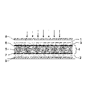
The invention will now be explained more closely by the description of
different embodiments
of the invention and with reference to the appended figures. Figure 1 shows a
cross section
through a dye-sensitized solar cell (DSC) according to an embodiment of the
invention. The DSC
disclosed in figure 1 is of a monolithic type. The DSC comprises a working
electrode 1 and a
counter electrode 2. The space between the working electrode and the counter
electrode is
filled with an electrolyte including ions for transferring electrons from the
counter electrode to
the working electrode. The DSC module comprises a conducting layer 3 for
extracting photo-
generated electrons from the working electrode 1. The conducting layer 3
serves as a back
contact and is in the following named the back contact layer. The working
electrode 1 includes
a porous T102 electrode layer disposed onto the back contact layer 3. The TiO2
electrode
comprises TiO2 particles dyed by adsorbing dye molecules on the surface of the
TiO2 particles.
The working electrode is positioned on a top side of the DCS module. The top
side should be
facing the sun to allow the sunlight to hit the dye molecules of the working
electrode.
The DSC module further includes a porous insulation substrate 4 arranged
between the
.. working electrode land the counter electrode 2. The porosity of the porous
insulation
substrate will enable ionic transport through the substrate. For example, the
porous insulation
substrate 4 is made of a ceramic microfiber, such as glass microfibers.
Substrates made of
ceramic microfibers are electrical insulators, but are porous and thereby
allowing liquids and
electrolyte ions to penetrate. The ceramic microfibers are cheap, chemically
inert, can
.. withstand high temperatures and are simple to handle in various process
steps.
The porous insulation substrate 4 comprises a layer of woven microfibers 5 and
a first layer of
non-woven microfibers 6 disposed on the layer of woven microfibers 5 on a
first side of the
substrate. This makes it possible to provide a thin and strong substrate. The
back contact layer
3 is a porous conducting layer disposed on the first side of the substrate on
the layer of non-
woven microfibers 6. in the embodiment disclosed in figure 1, the substrate
further comprises
a second layer of non-woven microfibers 7 disposed on the layer of woven
microfibers 5 on a
second side of the substrate. By providing layers of non-woven microfibers on
both sides of the
layer of woven microfibers, a symmetrical substrate is achieved. This may
prevent the
substrate from curling during the heat treatment during the manufacturing of
the solar cell,
CA 02866779 2014-11-25
,
12
and additionally contributes to prevent the particles in the printed ink to
pass through the layer
of woven microfibers. The porous insulation substrate 4 will be described in
more detail below
with reference to figure 5.
The counter electrode includes a conducting layer 2, in the following named
the counter
electrode layer. In this embodiment, the conducting layer 2 is a porous
conducting layer
disposed on the second side of the porous insulation substrate 4 on top of the
second layer of
non-woven microfibers 7. When a porous conducting layer is used as a counter
electrode, it is
part of the counter electrode opposite to the working electrode. The back
contact layer 3 and
the counter electrode layer 2 are separated physically and electrically by the
porous insulation
substrate 4. However, the back contact layer and the counter electrode layer
are electrically
connected via ions penetrating the porous insulation substrate. The porous
conducting layers
2,3 may be created using an ink including metallic or metal based particles,
which are applied
on top of the porous insulation layer 4 by printing, and followed by heating,
drying and baking.
The particles are typically between 0.1¨ 10 um. preferably between 0.5 ¨2 m.
The DSC also includes a first sheet 8 covering a top side of the DSC module
and a second sheet
9 covering a bottom side of the DSC module and acting as barriers in order to
protect the DSC
modules against the surrounding atmosphere, and to prevent the evaporation or
leakage of
the DSC components inside the cell. The first sheet 8 on the top side DSC
module covers the
working electrode and needs to be transparent, allowing light to pass through.
A thinner porous substrate is better, since a small distance between the
working electrode and
the counter electrode provides minimal losses in diffusion resistance of the
electrolyte.
However, if the substrate is too thin the mechanical strength of the substrate
will be too low.
Preferably, the thickness of the porous insulation substrate is larger than 4
km and less than
100 um. More preferably, the thickness of the porous insulation substrate is
less than 50 um.
The thickness of the porous insulation substrate is typically between 10 ¨ 30
um.
In the following, an example of porous insulating substrate according to the
invention will be
described in more details. The porous insulate substrate is based on a layer
of glass fabric
made of woven yarn including a plurality of glass fibers. Woven fibers are
much stronger than
CA 02866779 2014-11-25
13
non-woven fibers. Additionally, a layer of woven fibers can be thin with
maintained mechanical
strength.
Figure 2 shows an optical microscope picture of 15 pm thin glass fabric (Asahi
Kasei E-
materials). As can be seen in the figure, the glass fabric comprises woven
yarn 10a-b of glass
fibers. Each yarn includes a plurality of glass fibers, also denoted
filaments. The diameter of a
filament is typically 4 5 m, and the number of filaments in the yarn is
typically 50. The glass
fabric has large holes 14 between the woven yarns, which would allow a large
amount of the
conductive particles in the printed ink to pass right through the woven fiber
in an uncontrolled
way. This is an unwanted effect. The size of the holes can be as large as 200
p.m. In order to
block the holes in the fabric, non-woven glass fibers are disposed on top of
the fabric. This can
be done by soaking the fabric in a solution containing glass fibers and then
removing the liquid
part of the solution.
Figure 3 shows an optical microscope picture of the glass fabric shown in
figure 2 treated with
gram glass microfiber stock solution on both sides, corresponding to 0.04
milligrams of
15 deposited glass fiber per square centimeter on each side. As can be seen
in the figure, the
woven yarn in the glass fabric is covered by the disposed non-woven glass
fibers. It can also be
seen from figure 3 that the size of the holes in the fabric is reduced.
However, full coverage of
the holes in the glass fabric is not accomplished.
Figure 4 shows an optical microscope picture of the glass fabric shown in
figure 2 treated with
20 80 gram glass microfiber stock solution on both sides, corresponding to
0.16 milligrams of
deposited glass fiber per square centimeter on each side. As shown from figure
4, the holes are
now covered by the glass microfibers. Obviously, full coverage of holes in the
glass fabric can
be achieved by increasing the amount of glass microfiber. Thus, by depositing
non-woven glass
fibers on top of the woven glass fibers it is possible to prevent that
particles in the printed inks
pass right through the woven fibers.
If a binder such as, e.g., inorganic binders such as, silicates, colloidal
silica particles, silanes
(e.g., linear silane or branched silane or cyclic silane), and colloidal Al2O3
is added to the
fiberstock solution containing the glass fibers, the non-woven glass fibers
can stick stronger to
the woven fibers. Additionally, the layer consisting of deposited non-woven
will be stronger
CA 02866779 2014-11-25
,
,
14
mechanically as such. Consequently, by adding a binder to the fiberstock
solution it is possible
to form a mechanically strong non-woven layer that adheres strongly to the
woven glass fibers.
Example 1
In the following an example of a method for producing the porous substrate
shown in figure 4
will be described. A 15 p.m thin glass fabric (Asahi Kasei E-materials), as
shown in figure 2, with
50 filaments, with a filament diameter of 4 4m, was laid on top of a stainless
steel wire screen
(33 cm x 33 cm) in a hand sheet former and a stock cylinder was put on top of
the glass fabric
and then closed and tightened. A glass microfiber stock solution was prepared
by mixing 4000
grams of distilled water and 8 grams of glass microfibers (Johns Manville,
special purpose type
glass microfiber type 90, fiber diameter: 0.2 p.m) and 400 grams of water
based colloidal silica
(a solution containing around 15 wt.% SiO2 in water) such that the final
silica concentration
was 1.4 wt.%. The mixing was performed using an Ultraturrax batch dispenser.
The stock
cylinder of the hand sheet former machine was filled with distilled water
(containing 1.4 wt.%
silica) up to a level of 350 mm above the surface of the wire screen. In the
next step 80 grams
of glass microfiber stock was poured into the hand sheet former machine. The
glass fiber stock
and the distilled water containing silica were mixed by compressed air for 4
seconds and then
allowed to settle for 6 seconds, after which the water was drained through the
glass fabric and
the wire screen. The wet treated glass fabric was dried at 110 C in air in a
belt oven. The glass
fabric was then treated on the other side using the same process parameters as
in the first
treatment. The resulting substrate is shown in figure 4. As can be seen in
figure 4, the woven
yarn in the glass fabric is fully covered by the disposed non-woven glass
microfibers. The
thickness of the glass fabric with disposed glass microfibers was around 30
p.m. This means that
the total thickness of the two layers of non-woven microfibers is about 15 m.
By using a
thinner glass fabric, it is possible to further reduce the thickness of the
insulation substrate.
Example 2
A variation of Example 1 is that the microfiber stock solution is prepared by
mixing 4000 grams
of distilled water and 200 grams of nanocellulose dispersion (water based
nanocellulose
dispersion containing 2% by weight of nanocellulose) and 400 grams of water
based colloidal
silica (a solution containing 15 wt.% Si02 in water). Thus, the ceramic glass
microfibers in the
CA 02866779 2014-11-25
,
microfiber stock solution are replaced by organic microfibers consisting of
nanocellulose. Using
nanocellulose simplifies the manufacturing process in that dipping can be used
instead of using
a paper manufacturing process.
Example 3
5 Another variation of example 1 is that the microfiber stock solution is
prepared by mixing 4000
grams of distilled water and 2 grams of glass microfibers (Johns Manville,
special purpose type
glass microfiber type 90, fiber diameter: 0.21.tm) and 200 grams of
nanocellulose dispersion
(water based nanocellulose dispersion containing 2% by weight of
nanocellulose) and 400
grams of water based colloidal silica (a solution containing 15 wt.% SiO2 in
water). Thus, both
10 organic microfibers consisting of nanocellulose and ceramic microfibers
consisting of glass are
used in the microfiber stock solution. After the porous insulation substrate
has been dried, ink
with conductive particles is deposited on at least one side of the substrate
on top of the layer
of non-woven microfibers, to form a porous conducting layer on the porous
insulation
substrate. If a monolithic DCS module is to be manufactured, the ink is
deposited on both sides
15 of the substrate on top the layers of non-woven microfibers, to form a
porous conducting layer
on each side of the porous insulation substrate. However, if a sandwich type
DCS module is to
be manufactured, the ink with conductive particles is only deposited on one
side of the
substrate.
To make sure that the fibers in the microfiber stock solution is properly
dispersed it is
advantageous to add additives to the distilled water before mixing water and
the microfibers.
Examples of suitable additives are surfactants, dispersants, wetting agents,
retention aids,
defoamers, and rheology changing agents. It is advantageous to add one or more
of those
additives. The additives are burnt away during the following steps of the
manufacturing
process of the solar cell, and consequently do not remain in the end product.
The purpose of
the additives is to achieve individual and non-agglomerated fibers, so that
the individual fibers
can be deposited as homogeneously as possible in order to provide a thin and
at the same time
dense layer of individual fibers. Thus, by using additives, it is possible to
manufacture a thinner
and denser substrate with smaller holes.
CA 02866779 2014-11-25
,
16
By adding surfactants to the fiberstock solution and to the dilution water, a
smoother and
more homogeneous microfiber deposition can be accomplished. Further, it is
advantageous to
add a wetting agent to the fiberstock solution so that the dilution water wets
the fibers and the
fabric. Also, by adding a water soluble polymer to the fiberstock solution and
the dilution
water, a smoother and more homogeneous microfiber deposition can be
accomplished.
However, it was found that, when adding polymer it was necessary to add a
defoaming agent
in order to avoid excessive foaming during dilution water filling and
agitation and draining
cycles. It is also advantageous to add rheology changing additives to change
the viscosity of the
fiberstock solution and the dilution water.
It is also possible to add binders to the fiberstock solution and the dilution
water to enhance
the binding of non-woven fibers to each other and to enhance the binding of
non-woven fibers
to the fabric. Binders that can be used are e.g. inorganic binders such as,
silicates, colloidal
silica particles, silane, e.g. linear silane, branched silane, or cyclic
silane, and colloidal A1203.
It is also possible to add retention aids to the fiberstock solution and the
dilution water to
improve the retention of the fibers in the porous insulation substrate as it
is being formed.
Nanocellulose can be used as a retention aid.
Figure 5 shows a cross section through a porous insulation substrate 4
manufactured according
to the method described in the example described above. The substrate has a
layer 5 of woven
microfibers including woven yarns 10 comprising a plurality of filaments 11
and holes 14
formed between the yarns 10. The woven yarns 10 are preferably made of ceramic
microfibers.
The substrate also includes two layers 6, 7 of non-woven microfibers arranged
on each side of
the layer 5 of woven microfibers. The layers 6, 7 of non-woven microfibers can
be made of
ceramic microfibers, organic microfibers or a combination thereof. As can be
seen from the
figure, a main part of the non-woven microfibers are accumulated in the holes
14 between the
yarns 10. This is a consequence of the fact that the liquid from the
fiberstock solution is
drained through the holes formed in the fabric. This leads to that the
thickness of the non-
woven layers 6, 7 of microfibers varies in dependence of the locations of the
holes 14 in the
woven layer of microfibers, such that the non-woven layer is thicker in the
holes 14 in the
woven layer and thinner on top of the yarns 17 of the woven layer. The side of
the non-woven
CA 02866779 2014-11-25
17
layer 6, 7 that faces away from the woven layer 5 is smooth, but the opposite
side of the non-
woven layer that faces against the woven layer is uneven and has thick parts
16 that protrude
into the holes 14 of the woven layer and thin parts 17, which are disposed on
top of the yarns
10.The present invention can be used for monolithic as well as sandwich types
of DCS.
The non-woven microfibers should preferably be thinner than the filaments in
the layer of
woven microfibers. Thus, if the diameter of the filaments is about 4 m, the
fibers in the layer
of non-woven microfibers should have a diameter less than 4 ium, preferably
less than 1 km,
and more preferably less than 0.5 pm in order to block the holes in an
efficient way. The length
of the non-woven fibers is, for example 100 nm ¨3 mm. For example, the
diameter of nano-
cellulose fibers is typically 5 ¨ 10 nm and the length of the fibers is
typically several p.m.
However, there also exist nano-cellulose fibers having a diameter of 10 ¨ 20
nm and a length of
several mm.
The present invention is not limited to the embodiments disclosed but may be
varied and
modified within the scope of the following claims. For example, the microfiber
stock solution
.. may include microfibers of different materials and diameters. Although, the
examples above
use glass microfibers, the invention is not limited to glass microfibers. It
is possible to use other
types of ceramic microfibers with similar properties. Further, the microfibers
in the non-woven
layer can be made of a different ceramic material than the microfibers in the
woven layer.
Further, the microfibers in the non-woven layer can be made of organic
microfiber such as
cellulose or polymer.
In an alternative embodiment, the substrate may include a layer of non-woven
microfibers and
a layer of woven microfibers laminated together.
In an alternative embodiment, the substrate has only one layer of non-woven
microfibers,
arranged on one side of a layer of woven microfibers. Although it is
advantageous to have non-
woven layers on both sides of the woven layer, it is not necessary. It is
possible to deposit
conducting layers on both sides of the substrate although only one of the
sides of the woven
layer has been provided with a layer of non-woven microfibers. The conducting
layer can be
printed on the non-woven layer as well as on the woven layer. A substrate
having non-woven
CA 02866779 2014-11-25
g
18
layers deposited on both sides of the woven layer can be covered with a
conducting layer on
one side as well as on both sides.
In an alternative embodiment, the porous insulation substrate has only one
layer of non-woven
microfibers, arranged on one side of a layer of woven microfibers and the
conducting layer is
deposited on the other side of the woven microfibers, i.e. the conducting
layer is deposited on
the woven microfibers and not on the non-woven microfibers.
The porous insulating substrate is a porous and chemically inert and high
temperature resistant
and electrically insulating material that can be used for other applications
than in dye-
sensitized solar cells. The substrate can be used in filtering/filter
applications for removing, e.g.
dust, organic or inorganic or biological micro particles, flour, sand, smoke,
bacteria, and pollen.
The substrate can also be used as a separator, materially separating the
cathode and anode in
electrochemical- or photoelectrochemical devices such as fuel cells,
batteries, electrochemical
sensors, electrochromic displays, and photoelectrochemical solar cells.