Note: Descriptions are shown in the official language in which they were submitted.
CA 02871164 2014-10-22
W02014/023386 1
PCT/EP2013/002040
10
Insertion-type connector
The invention relates to a (multiple) insertion-type connector having a
housing
and a plurality of pairs of contact elements fixed in the housing which are
designed to make contact with complementary pairs of contact elements of an
mating insertion-type connector.
The invention relates in particular to a multiple insertion-type connector
suitable
for the transmission of radio-frequency signals (RF signals).
A problem which is posed by multiple insertion-type connectors of this kind is
to
prevent crosstalk between the plurality of pairs of contact elements and the
interference with signal transmission which goes hands in hand with this. For
this
purpose, it is known for shielding to be incorporated in the housing of the
insertion-type connector, with provision being made for the entire
circumference
of each pair of contact elements to be surrounded by the shielding to enable a
good shielding effect to be achieved. However, designing a multiple insertion-
type connector in this way results in relatively high production costs.
Taking the above prior art as a point of departure, the object underlying the
invention was to specify a multiple insertion-type connector which, while its
CA 02871164 2014-10-22
W02014/023386 2
PCT/EP2013/002040
transmission characteristics for RF signals remained good, could be produced
particularly inexpensively.
This object is achieved by an insertion-type connector as defined in
independent
claim 1. Advantageous embodiments of insertion-type connectors according to
the invention form the subject matter of the dependent claims and can be seen
from the following description of the invention.
The idea on which the invention is based is to reduce the production costs of
an
insertion-type connector of the generic kind by means of an advantageous
layout
for the pairs of contact elements in the housing, the layout being intended to
keep crosstalk between the pairs of contact elements as low as possible, to
ensure as simple a geometric shape as possible for the housing, and also to
make it possible for crosstalk between the pairs of contact elements to be
kept
low by the use of only one shielding element of as simple a design as
possible.
This idea behind the invention is put into practice as a structure by an
insertion-
type connector having a housing and a plurality of pairs of contact elements
fixed
in the housing, in which at least two pairs of contact elements are arranged
in
adjacent positions in a (first) row and at least one pair of contact elements
is
arranged to be spaced aside from the (first) row at identical spacings from
the
(most closely adjacent) pairs of contact elements, and a shielding element is
arranged between the pairs of contact elements in the (first) row on the one
hand
and the further pair of contact elements on the other hand (where a plurality
of
pairs of contact elements spaced from the (first) row are provided, they are
preferably arranged in a second row spaced from the first one, in parallel,
and
the spacings from the most closely adjacent pairs of contact elements in the
first
row are substantially identical to each other).
What can be achieved by the zigzag layout according to the invention of the
pairs of contact elements is that, in a preset volume of space, the spacing
between all the adjacent pairs of contact elements is as large as possible.
Crosstalk between the individual pairs of contact elements can already be kept
CA 02871164 2014-10-22
W02014/023386 3
PCT/EP2013/002040
relatively low by this means. This is further improved by the arranging of the
shielding element (e.g. a shielding plate) between the (first) row of pairs of
contact elements and the further pair of contact elements or between the two
rows of pairs of contact elements, as the case may be. The shielding element,
which preferably does not surround the entire circumference of any of the
pairs
of contact elements (around a direction of insertion of the individual contact
elements), may thus be of a geometrically simple configuration but, in
conjunction with the layout according to the invention of the pairs of contact
elements, is nevertheless able to produce a sufficiently good shielding
effect.
The layout according to the invention of the elements intended for signal
transmission may preferably be provided throughout the housing of the
insertion-
type connector, meaning that even conductors which are connected to the
individual contact elements are preferably arranged in the relevant layout in
a
(first) row and spaced therefrom (possibly in a second row). These conductors
may for example be conductors of cables (and in particular of twisted-pair
cables) which have an electrically conductive connection to the contact
elements. Similarly, what may also be incorporated in the housing are
conductors which for example project out of the housing for a short distance
at
their free ends. An insertion-type connector of this kind is then particularly
suitable for connection to a printed circuit board, with the free ends of the
conductors then making contact with corresponding pads on the printed circuit
board. In this case the insertion-type connector according to the invention
may
serve to connect to a printed circuit board a plurality of cables which are
connected to contact elements complementary to the contact elements of the
insertion-type connector.
Provision may also be made in this case for the conductors to follow an angled
path in the housing. Provision is preferably then made for a shielding element
(also) to be arranged between those portions of the conductors in the (first)
row
which are angled relative to the contact elements and the corresponding
portion(s) of the conductor(s) (in the second row) which is/are spaced from
the
(first) row. The shielding element may thus be of a form matching the
shielding
CA 02871164 2014-10-22
W02014/023386 4
PCT/EP2013/002040
element which is provided between the pairs of contact elements in the (first)
row
and the pairs of contact elements which are arranged at a spacing therefrom.
The possibility also exists of the two shielding elements being formed in one
piece, e.g. as an angled shielding plate.
The invention is explained in detail below by reference to an embodiment which
is shown in the drawings. In the drawings:
Fig. 1 is a first perspective view of an insertion-type connection
comprising an
insertion-type printed circuit board connector and a multiple insertion-
type connector.
Fig. 2 is a second perspective view of the insertion-type connection shown
in
Fig. 1.
Fig. 3 is a perspective view of the multiple insertion-type connector.
Fig. 4 is a perspective view of an individual insertion-type connector of
the
multiple insertion-type connector.
Fig. 5 is a perspective view of a part of the individual insertion-type
connector
shown in Fig. 4.
Fig. 6 is a perspective view of a part of the individual insertion-type
connector
shown in Fig. 4.
Fig. 7 is a first perspective view of the insertion-type printed circuit
board
connector.
Fig. 8 is a second perspective view of the insertion-type printed circuit
board
connector.
CA 02871164 2014-10-22
W02014/023386 5
PCT/EP2013/002040
Fig. 9 is a
perspective view of individual parts of the insertion-type printed
circuit board connector.
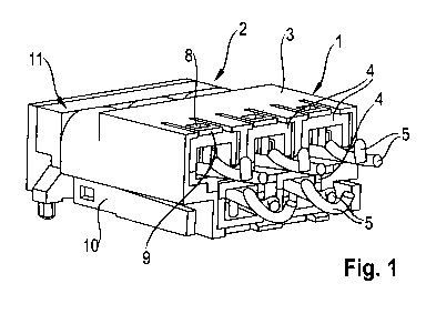
Figs. 1 and 2 show an insertion-type connection comprising a (multiple)
insertion-
type printed circuit board connector 2 according to the invention and a
multiple
insertion-type connector 1 which is used with it as a mating insertion-type
connector.
The multiple insertion-type connector 1 comprises a housing 3 which has a
plurality (a total of five in the present embodiment) of receiving openings
arranged in parallel. One insertion-type connector 4 according to the
invention
having a twisted-pair cable (of which only portions of the cores 5 are shown)
connected to it is inserted in each of these receiving openings and is secured
in
position therein by a latching connection. The latching connection is formed
in
each case by a projection 6 which is formed on an outer side of a housing 7 of
the given insertion-type connector 4, and by an undercut in the form of a
through-opening 8 which is formed in a tongue for latching 9 on the housing 3
of
the multiple insertion-type connector 1. As the insertion-type connectors 4
are
inserted in the receiving openings, the projections 6, which slope up
obliquely,
deflect the tongues for latching 9 until the projections 6 engage in the
through-
openings 8 in the latching tongues 9. To release the latching connection, it
is
possible for the given tongue for latching 9 to be raised manually and thus
brought out of engagement with the associated projection.
The housing 7 of the multiple insertion-type connector 1 also comprises two
lateral tongues for latching 10 which are intended to make a latching
connection
to a housing 11 of the insertion-type printed circuit board connector 2, which
has
for this purpose projections 12 which slope up obliquely in the appropriate
way.
Figs. 4 to 6 are views which show, in isolation, one of the insertion-type
connectors 4 according to the invention together with the twisted cores 5
(electrically conductive conductors and insulating sheaths) of a twisted-pair
cable
which is connected thereto. As well as the housing 7, the insertion-type
CA 02871164 2014-10-22
W02014/023386 6
PCT/EP2013/002040
connector 4 also comprises two contact elements 13 which are mounted in the
housing 7 in a fixed position (at least in the direction defined by their
longitudinal
axes) and which have insertion and cable ends. At their cable ends, the
contact
elements 13 are connected by crimped connections to stripped portions of
respective ones of the two cores 5 of the twisted-pair cable. The insertion
ends
are designed to make contact with complementary contact elements 14 of the
insertion-type printed circuit board connector 2, the contact elements 13 in
socket form of the insertion-type connector 4 receiving contact elements 14 in
pin
form of the insertion-type printed circuit board connector 2 and in so doing
being
expanded elastically in the radial direction, which is possible due to
appropriate
longitudinal slots.
The fixing of the contact elements 13 in position in the housing 7 is effected
by
respective surrounding projections 15 which are arranged in surrounding
grooves in the housing 7.
The housing 7 of the insertion-type connector 4 comprises two parts 16, 17.
The
plane of division between these parts 16, 17 of the housing extends in this
case
in parallel with, and in particular co-planarly with, that plane which is
defined by
the longitudinal axes of the two contact elements 13. A long-lasting
connection
between the two parts 16, 17 of the housing is obtained by means of two
tongues for latching 18 on a first one (16) of the parts of the housing, in
whose
undercuts (in the form of through-openings 19) projections 20 on the second
one
(17) of the part of the housing engage. There are also two projections 21 on
the
first part 16 of the housing which engage in complementary depressions 22 in
the second part 17 of the housing and which serve as an additional means of
securing the two parts 16, 17 of the housing in position relative to one
another.
The cores 5 of the twisted-pair cable extend along a twisted path even within
the
housing 7 of the insertion-type connector 4. For the cores 5, the housing 7
forms
a guide which ensures that the twist is permanent and cannot come untwisted.
The guidance so provided is achieved by means of the inner walls of a guiding
space formed by the housing 7, acting in conjunction with two guiding spigots
23
CA 02871164 2014-10-22
W02014/023386 7
PCT/EP2013/002040
which extend in the guiding space in a direction perpendicular to the plane
defined by the longitudinal axes of the two contact elements and centrally
between these two longitudinal axes. The guiding spigots 23 are formed in this
case by the second part 17 of the housing and, for stabilisation, engage in
depressions 24 in the first part 16 of the housing. Continuing the twisted
path
along which they are guided within the twisted-pair cable, the cores 5 of the
cable are guided round the guiding spigots 23 in arcs, and are thus looped
partway round them. Provision may also be made in this case for at least
portions of the cores 5 to be clamped in, at respective points, between the
guiding spigots 23 and the inner walls of the guiding space of the housing 7
or
between the inner walls of the housing 7 and whichever is the other core 5.
Relatively high tensile loads can thus be transmitted by the twisted-pair
cable to
the housing 7. This thus provides strain relief for the crimped connections
between the cores 5 and the contact elements 13.
The two parts 16, 17 of the housing of the insertion-type connector 4 are
formed
entirely of electrically non-conductive plastics material, with the simple
geometrical shape making advantageous injection moulding possible. In a
demoulding direction which is aligned in the direction defined by the
longitudinal
axes of the guiding spigots 23, only the first half 16 of the housing has
undercuts,
in the form of the through-openings 19 in the tongues for latching 18.
However,
because the tongues for latching 18 are designed to be elastically deflectable
precisely because of their function, it is possible even for the first part 16
of the
housing to be demoulded without the use of sliders or the like.
Separate shielding is not provided for the insertion-type connector 4.
However,
crosstalk between the individual insertion-type connectors 34 which are
combined in the multiple insertion-type connector 1 is sufficiently low for
many
applications due to the twist of the conductors 5, which continues as far as
the
contact elements 13.
Figs. 7 to 9 are various perspective views of the insertion-type printed
circuit
board connector, showing it in isolation. Said connector comprises the housing
CA 02871164 2014-10-22
W02014/023386 8
PCT/EP2013/002040
11 which has a main body 25 and a cover 26. On one side, the main body 25
forms an interface for insertion which is complementary to an interface for
insertion formed by the multiple insertion-type connector 1. The interface for
insertion of the insertion-type printed circuit board connector 2 comprises a
plurality (five in fact) of (through) openings 27 within each of which are
arranged
two contact elements 14 in pin form, i.e. a pair of contact elements, aligned
in
parallel. These latter, when the insertion-type connectors 1, 2 are in the
plugged-
together state, make contact with the contact elements 13 of the multiple
insertion-type connector 1. The cross-section of the openings 27 in the main
body 25 is that of an elongated oval and corresponds to the cross-section of
an
insertion portion 28 of the housings 7 of the individual insertion-type
connectors
4 of the multiple insertion-type connector 1. The (insertion) portion 29 of
the
outside of the main body 25, which (insertion) portion surrounds the openings,
is
of a complex shape which is complementary to the inside of an insertion
portion
30 of the housing 3 of the multiple insertion-type connector 1. The insertion
portions 28 of the individual insertion-type connectors 4 thus engage in the
openings 27 in the main body 25 of the insertion-type printed circuit board
connector 2 and the insertion portion 29 of the main body 25 of the insertion-
type
printed circuit board connector 2 engages in the insertion portion 30 of the
housing 3 of the multiple insertion-type connector 1. In conjunction with the
long-
lasting fixing by the tongues for latching 10, a high mechanical load-bearing
capacity can thus be obtained for the insertion-type connection.
The contact elements 14 of the insertion-type printed circuit board connector
2
are integrally formed at the insertion ends of conductors 31, which latter
initially
extend on for a defined distance into the main body 25 co-axially to the
contact
elements 14 and are then bent away through 90 . Those portions of the
conductors 31 which are angled away from the contact elements 14 are received
in slotted openings 32 in the cover 26, and they project beyond the cover 26
and
hence the housing 11 of the insertion-type printed circuit board connector 2
in
this case by a defined amount. By the projecting ends, the conductors 31 are
able to make contact with corresponding pads on a printed circuit board (not
shown), these ends preferably engaging at the same time in openings in the
CA 02871164 2014-10-22
W02014/023386 9
PCT/EP2013/002040
printed circuit board in order to connect the insertion-type printed circuit
board
connector 2 to the printed circuit board mechanically as well. Two projections
33
in spigot form which engage in corresponding openings in the printed circuit
board are used to provide further mechanical stabilisation.
The layout of the openings 27 and hence of the pairs of contact elements too
in
the housing 11 of the insertion-type printed circuit board connector 2 is of a
zigzag form, i.e. three of the five pairs of contact elements are arranged in
a first
row and the two remaining pairs of contact elements are arranged in a second
row spaced from the first row in parallel therewith. Provision is made in this
case
for the spacings of the two pairs of contact elements in the second row from
the
two pairs of contact elements respectively adjacent to them in the first row
to be
substantially the same, thus putting the latter in central positions relative
to the
former. A compact layout can thus be achieved for the pairs of contact
elements
in the housing 11, with as large a spacing as possible from adjacent pairs of
contact elements being maintained at the same time. Relatively low crosstalk
between the pairs of contact elements can thus be achieved simply by virtue of
the geometry.
Such crosstalk is also reduced by a shielding element in the form of a
shielding
plate 34 which is arranged in a slotted receptacle in the main body 25 which
extends between the first row and second row of pairs of contact elements. The
configuration of the receptacle, and hence of shielding plate 34, is not plane
in
this case but of a zigzag form, corresponding to the layout of the pairs of
contact
elements.
As can be seen from Fig. 9 in particular, the shielding plate 34 is also
angled
through 90 and thus follows the path followed by the conductors 31. At the
same time, that portion of the shielding plate 34 which extends at an angle to
the
contact elements 14 separates the relevant portions of the conductors 31 into
a
first row and a second row, the conductors 31 in the first row also forming
the
contact elements 14 in the first row and the conductors 31 in the second row
also
forming the contact elements 14 in the second row. This layout in three
CA 02871164 2014-10-22
W02014/023386 10
PCT/EP2013/002040
dimensions for the portions of the conductors 31 which are angled relative to
the
contact elements 14 is achieved by making the conductors 31 in the first row
on
the one hand and in the second row on the other hand of different lengths.
The shielding plate 34 also forms contact tabs which are intended to make
contact with shielding contacts on the printed circuit board.
The main body 25 and the cover 26 of the insertion-type printed circuit board
connector 2 are formed entirely of electrically non-conductive plastics
material,
with the geometrically simple shape of the two components simplifying
manufacture by injection moulding. The shielding plate 34 which is angled
through 90 is likewise of a geometrically simple shape which makes production
as a stamped, punched or die-cut, and bent component easy and inexpensive.