Note: Descriptions are shown in the official language in which they were submitted.
CA 02871779 2014-10-27
WO 2013/173507 PCT/US2013/041228
1
Crosstalk suppression in a directional backlight
TECHNICAL FIELD
[0001] This disclosure generally relates to illumination of light modulation
devices, and more
specifically relates to means for control of stray light in light guides for
providing large area
illumination from localized light sources for use in 2D, 3D, and/or
autostereoscopic display
devices.
BACKGROUND
[0002] Spatially multiplexed autostcreoscopic displays typically align a
parallax component such
as a lenticular screen or parallax barrier with an array of images arranged as
at least first and
second sets of pixels on a spatial light modulator, for example an LCD. The
parallax component
directs light from each of the sets of pixels into different respective
directions to provide first and
second viewing windows in front of the display. An observer with an eye placed
in the first
viewing window can see a first image with light from the first set of pixels;
and with an eye
placed in the second viewing window can see a second image, with light from
the second set of
pixels.
[0003] Such displays have reduced spatial resolution compared to the native
resolution of the
spatial light modulator and further, the structure of the viewing windows is
determined by the
pixel aperture shape and parallax component imaging function. Gaps between the
pixels, for
example for electrodes, typically produce non-uniform viewing windows.
Undesirably such
displays exhibit image flicker as an observer moves laterally with respect to
the display and so
limit the viewing freedom of the display. Such flicker can be reduced by
defocusing the optical
elements; however such defocusing results in increased levels of image cross
talk and increases
visual strain for an observer. Such flicker can be reduced by adjusting the
shape of the pixel
aperture, however such changes can reduce display brightness and can include
addressing
electronics in the spatial light modulator.
BRIEF SUMMARY
[0004] According to a first aspect of the present disclosure, there is
provided a directional
backlight for a transmissive spatial light modulator which may include a
waveguide. The
waveguide may have an input end, first and second opposed guide surfaces for
guiding light
along the waveguide, and a reflective end facing the input end for reflecting
light from the input
CA 02871779 2014-10-27
WO 2013/173507 PCMJS2013/041228
2
light back through the waveguide. The directional backlight may also include
an array of light
sources arranged to output light predominantly in an emission band and in a
conversion band.
The light sources may be disposed at different input positions in a lateral
direction across the
input end of the waveguide. The waveguide may be arranged to direct input
light from light
sources, at the different input positions across the input end, as output
light through the first
guide surface after reflection from the reflective end for supply through a
transmissive spatial
light modulator into optical windows in respective output directions. The
output directions may
be distributed in the lateral direction in dependence on the input positions.
The directional
backlight may also include a reflection reduction element arranged to reduce
reflections of light
incident on the input end after reflection from the reflective end.
[0005] Light reflected from the reflective end and incident on the input end
generally is lost from
the system, reducing overall system efficiency. However, some of the light
incident on the input
end after reflection from the reflective end may be further reflected back
into the waveguide by
means of Fresnel reflections at the input end rather than exiting the
waveguide, which may be
referred to herein as reflection artifacts. The present embodiments may reduce
image artifacts
that may be otherwise achieved by the further reflected light. In particular,
undesirable image
cross talk may be reduced so that autostereoscopic 3D images with increased
depth and reduced
visual strain may be produced by the display. Further, line artifacts arising
from said multiple
reflections of rays at the input end may be reduced or eliminated.
[0006] The reflection reduction element may take various forms.
[0007] The reflection reduction element may be a light diffusing element which
may have
asymmetric light diffusing properties.
[0008] Advantageously, the diffuser may reduce reflection artifacts arising
from specular
reflections at the input end and thus achieve a reduction in line artifacts by
increasing the angular
spread of the reflected light so that line artifacts are distributed across
the display area and
visibility is minimized. The asymmetric diffusing properties may achieve an
angular spreading
of the light in the x-y plane, with reduced spreading in the x-z plane, thus
reducing light loss for
input light from the light sources at the input end.
[0009] In one example, the reflection reduction element may be a linear
polarizer, in which case
the directional backlight may further include a phase retarder element at the
reflective end.
CA 02871779 2014-10-27
WO 2013/173507 PCMJS2013/041228
3
[0010] Advantageously the linear polarizer and phase retarder may cooperate to
rotate the
polarization of light from the light sources, so that the reflected light
incident on the input end is
absorbed by the input polarizer before Fresnel reflection that may occur at
the input end if that
end were to be in air. Thus the undesirable reflection artifacts are reduced,
improving image
quality and reducing image artifacts.
[0011] In another example, the reflection reduction element may cover at least
the light sources
and may be operable so that portions of the reflection reduction element
adjacent respective light
sources may selectively transmit light when the respective adjacent light
source is operated and
otherwise may absorb light incident on the input end after reflection from the
reflective end.
[0012] Advantageously, the regions of the input end in alignment with
operating light sources
may achieve high throughput efficiency and regions not in alignment with the
operating light
sources may achieve high absorption, reducing the reflection artifacts for
light reflected from the
input end in the respective regions not in alignment with the operating light
sources.
[0013] The reflection reduction element may include a filter, which may be
disposed between
the input end and the light sources, and arranged to absorb light in the
conversion band
preferentially over light in the emission band.
[0014] Some of the light that is reflected from the reflective end and is then
incident on the input
end may be transmitted by the input end and be incident on the light source.
Such light may be
scattered and reflected by elements of the light source and be directed back
into the waveguide.
Such light can produce undesirable visual artifacts including cross talk.
Typically the conversion
element such as a phosphor of a light source may be reflective to light in the
conversion band,
and may have a relatively large area in comparison to the emission element
such as a
semiconductor emitter of the light source. Advantageously the filter may
reduce the intensity of
reflected light from the light source preferentially for light in the
conversion band, thus the
reflectivity of the light source for the larger part of its emitting area may
be preferentially
reduced while enabling transmission of light in the emission band. Further,
input light in the
conversion band from the light source undergoes a single pass through the
filter, whereas
reflected light has a double pass; thus the reflected light is preferentially
absorbed in comparison
to the input light. The visual artifacts arising from scattering and
reflection of reflected light at
the light source may be reduced.
CA 02871779 2014-10-27
WO 2013/173507 PCMJS2013/041228
4
[0015] The reflection reduction element may include at least one light
absorbing element
covering part of the area of the respective light source and arranged to
absorb light after
reflection from the reflective end. The at least one light absorbing element
may be disposed
between the input end and each of the light sources.
[0016] Reflected light may be thus be absorbed by the input filter over part
of the light source,
reducing the intensity of reflection artifacts from the light source. Input
light may further be
recycled by the optical filter whereas reflected light may be absorbed by the
input filter.
Advantageously the intensity of the input light may be enhanced in comparison
to uniform filters
whereas a portion of the reflected light may be absorbed, thus reducing
reflectivity of the light
source and reducing visual artifacts.
[0017] According to a second aspect of the present disclosure, there may be
provided a light
source including a substrate, a light generation element supported on the
substrate which may be
arranged to generate light in an emission band, and a wavelength conversion
material supported
on the substrate. The wavelength conversion material may be arranged to
convert light in the
emission band generated by the light generation element substantially into
light in a conversion
band. The substrate may be colored to reflect the emission band preferentially
over the
conversion band.
[0018] Light output from the light source may be incident on the package of
the light source
after a reflection, for example in waveguide which the light source
illuminates. Desirably, the
reflectivity of the light source to the reflected light is reduced. The
package may achieve a high
reflectivity for light in the emission band and low reflectivity for light in
the conversion band.
Emitted light in the emission band may be reflected by the package, and
forward scattered light
in the conversion band may be outputted from the package without substantial
reflections from
the package, achieving high output efficiency of the package. Reflected light
in the conversion
band may be absorbed by the package. Reflected light in the emission band may
be further
converted by the conversion element and absorbed by the package.
Advantageously, high output
efficiency may be achieved while high absorption of reflected light may be
achieved, reducing
reflection artifacts.
[0019] According to a third aspect of the present disclosure, there may be
provided a directional
backlight for a transmissive spatial light modulator, which may include a
waveguide. The
waveguide may have an input end, first and second opposed guide surfaces for
guiding light
CA 02871779 2014-10-27
WO 2013/173507 PCT/1JS2013/041228
along the waveguide, and a reflective end facing the input end for reflecting
light from the input
light back through the waveguide. The directional backlight may also include
an array of light
sources arranged to output light predominantly in an emission band and in a
conversion band.
The light sources may be disposed at different input positions in a lateral
direction across the
input end of the waveguide. The waveguide may be arranged to direct input
light from light
sources, at the different input positions across the input end, as output
light through the first
guide surface after reflection from the reflective end for supply through a
transmissive spatial
light modulator into respective optical windows in output directions. The
output directions may
be distributed in the lateral direction in dependence on the input positions.
The light sources may
have respective light emitting regions having a width, in a direction along
the input end in which
the light sources are arrayed, which is approximately at or below 50% of the
pitch of the light
sources.
[0020] The emitting region may be advantageously arranged to have high output
efficiency and
luminous emittance. The area of the light source is reduced and gaps between
the light sources
are absorbing so that the total area of reflecting light source may be reduced
and the total area
reflectivity correspondingly reduced. Advantageously the reflection artifacts
may be reduced.
[0021] According to a further aspect of the present disclosure, there may be
provided an optical
valve for guiding light, which may include a first light guiding surface, and
a second light
guiding surface opposite the first light guiding surface. The second light
guiding surface may
further include a plurality of guiding features and a plurality of extraction
features The plurality
of extraction features may be operable to direct light to pass with
substantially low loss when the
light is propagating in a first direction. Further, the optical valve for
guiding light may include a
light input surface which may be located at a first end of the optical valve,
and at least one of the
light input surface or an array of illuminator elements may include at least
one reflection
reduction optical element.
[0022] According to a further aspect of the present disclosure, there may be
provided a stepped
imaging directional backlight, which may include a first light directing side
and a second light
directing side located opposite the first light directing side. The second
light directing side may
include a plurality of guiding features and a plurality of extraction
features. The plurality of
extraction features may be operable to direct light to pass with substantially
low loss when the
light is propagating in a first direction. The stepped imaging directional
backlight may further
CA 02871779 2014-10-27
WO 2013/173507 PCMJS2013/041228
6
include an array of illuminator elements located at a first end of the stepped
imaging directional
backlight, and the first end of the stepped imaging directional backlight may
be located between
the first and second light directing side. Additionally, at least one
reflection reduction optical
element may be located at the first end of the stepped imaging directional
backlight.
[0023] According to a further aspect of the present disclosure, there may be
provided a
directional illumination system which may include a light extraction element
for guiding and
extracting light. The light extraction element may include a first section
operable to allow light
rays to spread and a second section which may include a first light guiding
surface and a second
light guiding surface opposite the first light guiding surface. The second
light guiding surface
may include at least one guiding feature and a plurality of extraction
features and the extraction
features may direct light to exit the light extraction element. The light
extraction element may
further include a first illumination input surface located between the first
and second light
guiding surfaces. The first illumination input surface may be operable to
receive light from a
first array of light sources. The light extraction element may also include at
least one reflection
reduction optical element located at the first end of the light extraction
element.
[0024] According to a further aspect of the present disclosure, there may be
provided a
directional backlight display system which may include a first light
extraction element. The first
light extraction element may include a first light guiding surface and a
second light guiding
surface opposite the first light guiding surface. The second light guiding
surface may further
include a plurality of guiding features and a plurality of extraction
features. The plurality of
extraction features may direct light to pass with substantially low loss when
the light is
propagating in a first direction. The directional backlight display system may
include a spatial
light modulator proximate to the first light extraction element. Additionally,
the directional
backlight display system may include at least one reflection reduction optical
element located at
a first end of the first light extraction element.
[0025] According to the present disclosure, an optical valve for guiding light
may include a first
light guiding surface and a second light guiding surface opposite the first
light guiding surface.
The second light guiding surface may include a plurality of guiding features
and a plurality of
extraction features, in which the plurality of extraction features may be
operable to direct light to
pass with substantially low loss when the light is propagating in a first
direction. The optical
valve may further include a light input surface located at a first end of the
optical valve, in which
at least one of the light input surface or an array of illuminator elements
may include at least one
reflection reduction optical element.
[0026] Display backlights in general employ waveguides and edge emitting
sources. Certain imaging
directional backlights have the additional capability of directing the
illumination through a display
panel into viewing windows. An imaging system may be formed between multiple
sources and the
respective window images. One example of an imaging directional backlight is
an optical valve that
may employ a folded optical system and hence may also be an example of a
folded imaging directional
backlight. Light may propagate substantially without loss in one direction
through the optical valve
while counter-propagating light may be extracted by reflection off tilted
facets.
[0027] The present embodiments may achieve reduction of stray light
propagating within an imaging
directional backlight apparatus. In autostereoscopic display apparatus, such a
reduction advantageously
may achieve improved 3D image cross talk, greater viewing comfort and higher
image depth to be
presented. In privacy displays, a higher degree of separation of view data may
be provided, thus
improving the privacy function. In flat area cameras, higher contrast capture
may be achieved.
[0028] Embodiments herein may provide an autostereoscopic display with large
area and thin structure.
Further, as will be described, the optical valves of the present disclosure
may achieve thin optical
components with large back working distances. Such components can be used in
directional backlights,
to provide directional displays including autostereoscopic displays. Further,
embodiments may provide
a controlled illuminator for the purposes of an efficient autostereoscopic
display.
[0029] Embodiments of the present disclosure may be used in a variety of
optical systems. The
embodiment may include or work with a variety of projectors, projection
systems, optical components,
displays, microdisplays, computer systems, processors, self-contained
projector systems, visual and/or
audiovisual systems and electrical and/or optical devices. Aspects of the
present disclosure may be
used with practically any apparatus related to optical and electrical devices,
optical systems,
presentation systems or any apparatus that may contain any type of optical
system. Accordingly,
embodiments of the present disclosure may be employed in optical
7
Date Recue/Date Received 2021-08-06
CA 02871779 2014-10-27
WO 2013/173507 PC1'4182013/041228
8
systems, devices used in visual and/or optical presentations, visual
peripherals and so on and in a
number of computing environments.
[0030] Before proceeding to the disclosed embodiments in detail, it should be
understood that
the disclosure is not limited in its application or creation to the details of
the particular
arrangements shown, because the disclosure is capable of other embodiments.
Moreover,
aspects of the disclosure may be set forth in different combinations and
arrangements to define
embodiments unique in their own right. Also, the terminology used herein is
for the purpose of
description and not of limitation.
[0031] Directional backlights offer control over the illumination emanating
from substantially
the entire output surface controlled typically through modulation of
independent LED light
sources arranged at the input aperture side of an optical waveguide.
Controlling the emitted
light directional distribution can achieve single person viewing for a
security function, where the
display can only be seen by a single viewer from a limited range of angles;
high electrical
efficiency, where illumination is only provided over a small angular
directional distribution;
alternating left and right eye viewing for time sequential stereoscopic and
autostereoscopic
display; and low cost.
[0032] The various embodiments and/or aspects of the present disclosure may be
applied
together in any combination. It should be noted that the figures as
illustrated herein may not be
drawn to scale and are illustrated as such for discussion purposes only and
not of limitation.
[0033] These and other advantages and features of the present disclosure will
become apparent
to those of ordinary skill in the art upon reading this disclosure in its
entirety.
BRIEF DESCRIPTION OF THE DRAWINGS
[0034] Embodiments are illustrated by way of example in the accompanying
FIGURES, in
which like reference numbers indicate similar parts, and in which:
[0035] FIGURE 1A is a schematic diagram illustrating a front view of light
propagation in one
embodiment of a directional display device, in accordance with the present
disclosure;
[0036] FIGURE 1B is a schematic diagram illustrating a side view of light
propagation in one
embodiment of the directional display device of FIGURE 1A, in accordance with
the present
disclosure;
[0037] FIGURE 2A is a schematic diagram illustrating in a top view of light
propagation in
another embodiment of a directional display device, in accordance with the
present disclosure;
CA 02871779 2014-10-27
WO 2013/173507 PCMJS2013/041228
9
[0038] FIGURE 2B is a schematic diagram illustrating light propagation in a
front view of the
directional display device of FIGURE 2A, in accordance with the present
disclosure;
[0039] FIGURE 2C is a schematic diagram illustrating light propagation in a
side view of the
directional display device of FIGURE 2A, in accordance with the present
disclosure;
[0040] FIGURE 3 is a schematic diagram illustrating in a side view of a
directional display
device, in accordance with the present disclosure;
[0041] FIGURE 4A is schematic diagram illustrating in a front view, generation
of a viewing
window in a directional display device including curved light extraction
features, in accordance
with the present disclosure;
[0042] FIGURE 4B is a schematic diagram illustrating in a front view,
generation of a first and
a second viewing window in a directional display device including curved light
extraction
features, in accordance with the present disclosure;
[0043] FIGURE 5 is a schematic diagram illustrating generation of a first
viewing window in a
directional display device including linear light extraction features, in
accordance with the
present disclosure;
[0044] FIGURE 6A is a schematic diagram illustrating one embodiment of the
generation of a
first viewing window in a time multiplexed imaging directional display device
in a first time slot,
in accordance with the present disclosure;
[0045] FIGURE 6B is a schematic diagram illustrating another embodiment of the
generation of
a second viewing window in a time multiplexed directional display device in a
second time slot,
in accordance with the present disclosure;
[0046] FIGURE 6C is a schematic diagram illustrating another embodiment of the
generation of
a first and a second viewing window in a time multiplexed directional display
device, in
accordance with the present disclosure;
[0047] FIGURE 7 is a schematic diagram illustrating an observer tracking
autostereoscopic
display apparatus including a time multiplexed directional display device, in
accordance with the
present disclosure;
[0048] FIGURE 8 is a schematic diagram illustrating a multi-viewer directional
display device,
in accordance with the present disclosure;
[0049] FIGURE 9 is a schematic diagram illustrating a privacy directional
display device, in
accordance with the present disclosure;
CA 02871779 2014-10-27
WO 2013/173507 PCT/1JS2013/041228
[0050] FIGURE 10 is a schematic diagram illustrating in side view, the
structure of a time
multiplexed directional display device, in accordance with the present
disclosure;
[0051] FIGURE 11A is a schematic diagram illustrating a front view of a wedge
type
directional backlight, in accordance with the present disclosure;
[0052] FIGURE 11B is a schematic diagram illustrating a side view of a wedge
type directional
backlight, in accordance with the present disclosure;
[0053] FIGURE 12 is a schematic diagram illustrating a directional display
apparatus including
a display device and a control system, in accordance with the present
disclosure;
[0054] FIGURE 13 is a schematic diagram illustrating generation of viewing
windows from a
discontinuous array of illuminator elements, in accordance with the present
disclosure;
[0055] FIGURE 14 is a schematic diagram illustrating generation of viewing
windows from a
discontinuous array of illuminator elements, in accordance with the present
disclosure;
[0056] FIGURE 15 is a schematic diagram illustrating an origin of stray light
in a waveguide, in
accordance with the present disclosure;
[0057] FIGURE 16 is a schematic diagram illustrating generation of secondary
viewing
windows from stray light in a waveguide, in accordance with the present
disclosure;
[0058] FIGURE 17 is a schematic diagram illustrating a further illumination
artifact arising
from stray light in a waveguide, in accordance with the present disclosure;
[0059] FIGURE 18 is a schematic diagram illustrating a directional backlight
arranged to reduce
stray light propagation, in accordance with the present disclosure;
[0060] FIGURE 19 is a schematic diagram illustrating one embodiment of a
directional
backlight incorporating a stray light reduction arrangement, in accordance
with the present
disclosure;
[0061] FIGURE 20 is a schematic diagram illustrating the transmission spectrum
of one
example of a color absorption filter used in the directional backlight of
FIGURE 19, in
accordance with the present disclosure;
[0062] FIGURE 21 is a schematic diagram illustrating a detail of a further
directional backlight
incorporating a stray light reduction arrangement, in accordance with the
present disclosure;
[0063] FIGURE 22 is a schematic diagram illustrating an end view of the
directional backlight
of FIGURE 21, in accordance with the present disclosure;
CA 02871779 2014-10-27
WO 2013/173507 PCMJS2013/041228
11
[0064] FIGURE 23 is a schematic diagram illustrating a graph of a white light
source spectral
distribution, in accordance with the present disclosure;
[0065] FIGURE 24 is a schematic diagram illustrating a further directional
backlight
incorporating a stray light reduction arrangement, in accordance with the
present disclosure;
[0066] FIGURE 25 is a schematic diagram illustrating a detail of a further
directional backlight
incorporating a stray light reduction arrangement, in accordance with the
present disclosure;
[0067] FIGURE 26 is a schematic diagram illustrating a detail of a further
directional backlight
incorporating a stray light reduction arrangement, in accordance with the
present disclosure;
[0068] FIGURE 27 is a schematic diagram illustrating a directional backlight
arranged to
reduce stray light propagation, in accordance with the present disclosure;
[0069] FIGURE 28 is a schematic diagram illustrating a directional backlight
arranged to reduce
stray light propagation including a diffusing element, in accordance with the
present disclosure;
[0070] FIGURE 29 is a schematic diagram illustrating a directional backlight
arranged to reduce
stray light propagation including a diffusing element, in accordance with the
present disclosure;
[0071] FIGURE 30 is a schematic diagram illustrating an arrangement of
illuminator elements,
in accordance with the present disclosure;
[0072] FIGURE 31 is a schematic diagram illustrating a further arrangement of
illuminator
elements, in accordance with the present disclosure;
[0073] FIGURE 32 is a schematic diagram illustrating generation of yellow
stray light in a first
arrangement of illuminator elements, in accordance with the present
disclosure;
[0074] FIGURE 33 is a schematic diagram illustrating generation of blue stray
light in the first
arrangement of illuminator elements, in accordance with the present
disclosure;
[0075] FIGURE 34 is a schematic diagram illustrating generation of yellow
stray light in an
alternative arrangement of illuminator elements, in accordance with the
present disclosure;
[0076] FIGURE 35 is a schematic diagram illustrating generation of blue stray
light in the
alternative arrangement of illuminator elements, in accordance with the
present disclosure;
[0077] FIGURE 36 is a schematic diagram illustrating a illuminator element for
illuminating a
waveguide, including an ultra-violet illuminator element, in accordance with
the present
disclosure;
[0078] FIGURE 37 is a schematic diagram illustrating generation of stray light
in an alternative
arrangement of illuminator elements, in accordance with the present
disclosure;
CA 02871779 2014-10-27
WO 2013/173507 PCMJS2013/041228
12
[0079] FIGURE 38 is a schematic diagram illustrating in front view an
arrangement of
illuminator elements, in accordance with the present disclosure;
[0080] FIGURE 39 is a schematic diagram illustrating in side view, the
arrangement of
FIGURE 38, in accordance with the present disclosure;
[0081] FIGURE 40A is a schematic diagram illustrating in front view an
arrangement of
illuminator elements to provide reduced stray light in a waveguide, in
accordance with the
present disclosure;
[0082] FIGURE 40B is a schematic diagram illustrating in side view, the
arrangement of
FIGURE 40A, in accordance with the present disclosure;
[0083] FIGURE 41A is a schematic diagram illustrating in front view an
arrangement of
illuminator elements to provide reduced stray light in a waveguide, in
accordance with the
present disclosure;
[0084] FIGURE 41B is a schematic diagram illustrating in side view, the
arrangement of
FIGURE 41A, in accordance with the present disclosure;
[0085] FIGURE 42A is a schematic diagram illustrating in front view an
arrangement of
illuminator elements to provide reduced stray light in a waveguide, in
accordance with the
present disclosure;
[0086] FIGURE 42B is a schematic diagram illustrating in front view an
alternative
arrangement of illuminator elements to provide reduced stray light in a
waveguide, in accordance
with the present disclosure;
[0087] FIGURE 42C is a schematic diagram illustrating in side view, the
arrangement of
FIGURES 42A and 42B, in accordance with the present disclosure;
[0088] FIGURE 43A is a schematic diagram illustrating a first directional
backlight with a first
stray light contribution, in accordance with the present disclosure;
[0089] FIGURE 43B is a schematic diagram illustrating a second directional
backlight with a
second stray light contribution, in accordance with the present disclosure;
[0090] FIGURE 44 is a schematic diagram illustrating in front view an
arrangement of
illuminator elements to reduce stray light in a waveguide, in accordance with
the present
disclosure;
CA 02871779 2014-10-27
WO 2013/173507 PCMJS2013/041228
13
[0091] FIGURE 45 is a schematic diagram illustrating in front view an
alternative arrangement
of illuminator elements to reduce stray light in a waveguide, in accordance
with the present
disclosure;
[0092] FIGURE 46 is a schematic diagram illustrating at a first scale the
operation of a
waveguide including an input array of focusing optics, in accordance with the
present disclosure;
[0093] FIGURE 47 is a schematic diagram illustrating at a second scale the
operation of a
waveguide including an input array of focusing optics, in accordance with the
present disclosure;
and
[0094] FIGURE 48 is a schematic diagram illustrating at a third scale the
operation of a
waveguide including an input array of focusing optics and arranged to provide
reduced stray
light, in accordance with the present disclosure.
DETAILED DESCRIPTION
[0095] Time multiplexed autostereoscopic displays can advantageously improve
the spatial
resolution of autostereoscopic display by directing light from all of the
pixels of a spatial light
modulator to a first viewing window in a first time slot, and all of the
pixels to a second viewing
window in a second time slot. Thus an observer with eyes arranged to receive
light in first and
second viewing windows will see a full resolution image across the whole of
the display over
multiple time slots. Time multiplexed displays can advantageously achieve
directional
illumination by directing an illuminator array through a substantially
transparent time
multiplexed spatial light modulator using directional optical elements,
wherein the directional
optical elements substantially form an image of the illuminator array in the
window plane.
[0096] The uniformity of the viewing windows may be advantageously independent
of the
arrangement of pixels in the spatial light modulator. Advantageously, such
displays can provide
observer tracking displays which have low flicker, with low levels of cross
talk for a moving
observer.
[0097] To achieve high uniformity in the window plane, it is desirable to
provide an array of
illumination elements that have a high spatial uniformity. The illuminator
elements of the time
sequential illumination system may be provided, for example, by pixels of a
spatial light
modulator with size approximately 100 micrometers in combination with a lens
array. However,
such pixels suffer from similar difficulties as for spatially multiplexed
displays. Further, such
devices may have low efficiency and higher cost, requiring additional display
components.
CA 02871779 2014-10-27
WO 2013/173507 PCT/1JS2013/041228
14
[0098] High window plane uniformity can be conveniently achieved with
macroscopic
illuminators, for example, an array of LEDs in combination with homogenizing
and diffusing
optical elements that are typically of size 1 mm or greater. However, the
increased size of the
illuminator elements means that the size of the directional optical elements
increases
proportionately. For example, a 16 mm wide illuminator imaged to a 65 mm wide
viewing
window may require a 200 mm back working distance. Thus, the increased
thickness of the
optical elements can prevent useful application, for example, to mobile
displays, or large area
displays.
[0099] Addressing the aforementioned shortcomings, optical valves as described
in commonly-
owned U.S. Patent Application No. 13/300,293 advantageously can be arranged in
combination
with fast switching transmissive spatial light modulators to achieve time
multiplexed
autostereoscopic illumination in a thin package while providing high
resolution images with
flicker free observer tracking and low levels of cross talk. Described is a
one dimensional array
of viewing positions, or windows, that can display different images in a
first, typically
horizontal, direction, but contain the same images when moving in a second,
typically vertical,
direction.
[00100] Conventional non-imaging display backlights commonly employ optical
waveguides and have edge illumination from light sources such as LEDs.
However, it should be
appreciated that there are many fundamental differences in the function,
design, structure, and
operation between such conventional non-imaging display backlights and the
imaging directional
backlights discussed in the present disclosure.
[00101] Generally, for example, in accordance with the present disclosure,
imaging
directional backlights are arranged to direct the illumination from multiple
light sources through
a display panel to respective multiple viewing windows in at least one axis.
Each viewing
window is substantially formed as an image in at least one axis of a light
source by the imaging
system of the imaging directional backlight. An imaging system may be formed
between
multiple light sources and the respective window images. In this manner, the
light from each of
the multiple light sources is substantially not visible for an observer's eye
outside of the
respective viewing window.
[00102] In contradistinction, conventional non-imaging backlights or light
guiding plates
(LGPs) are used for illumination of 2D displays. See, e.g., Kalil Kalantar et
al., Backlight Unit
With Double Surface Light Emission, J. Soc. Inf. Display, Vol. 12, Issue 4,
pp. 379-387 (Dec. 2004).
Non-imaging backlights are typically arranged to direct the illumination from
multiple light sources
through a display panel into a substantially common viewing zone for each of
the multiple light sources
to achieve wide viewing angle and high display uniformity. Thus non-imaging
backlights do not form
viewing windows. In this manner, the light from each of the multiple light
sources may be visible for
an observer's eye at substantially all positions across the viewing zone. Such
conventional non-imaging
backlights may have some directionality, for example, to increase screen gain
compared to Lambertian
illumination, which may be provided by brightness enhancement films such as
BEFTM from 3M.
However, such directionality may be substantially the same for each of the
respective light sources.
Thus, for these reasons and others that should be apparent to persons of
ordinary skill, conventional
non-imaging backlights are different to imaging directional backlights. Edge
lit non-imaging backlight
illumination structures may be used in liquid crystal display systems such as
those seen in 2D Laptops,
Monitors and TVs. Light propagates from the edge of a lossy waveguide which
may include sparse
features; typically local indentations in the surface of the guide which cause
light to be lost regardless
of the propagation direction of the light.
[00103] As used herein, an optical valve is an optical structure that may be a
type of light guiding
structure or device referred to as, for example, a light valve, an optical
valve directional backlight, and
a valve directional backlight ("v-DBL"). In the present disclosure, optical
valve is different to a spatial
light modulator (even though spatial light modulators may be sometimes
generally referred to as a
"light valve" in the art). One example of an imaging directional backlight is
an optical valve that may
employ a folded optical system. Light may propagate substantially without loss
in one direction
through the optical valve, may be incident on an imaging reflector, and may
counter-propagate such
that the light may be extracted by reflection off tilted light extraction
features, and directed to viewing
windows.
[00104] As used herein, examples of an imaging directional backlight include a
stepped waveguide
imaging directional backlight, a folded imaging directional backlight, a wedge
type directional
backlight, or an optical valve.
[00105] Additionally, as used herein, a stepped waveguide imaging directional
backlight may be an
optical valve. A stepped waveguide is a waveguide for an imaging directional
backlight. The imaging
directional backlight may include a waveguide for guiding light, further
including a first light guiding
Date Re9ue/Date Received 2020-09-08
surface; and a second light guiding surface, opposite the first light guiding
surface, further including a
plurality of light guiding features interspersed with a plurality of
extraction features arranged as steps.
[00106] Moreover, as used, a folded imaging directional backlight may be at
least one of a wedge type
directional backlight, or an optical valve.
[00107] In operation, light may propagate within an exemplary optical valve in
a first direction from
an input end to a reflective end and may be transmitted substantially without
loss. Light may be
reflected at the reflective end and propagates in a second direction
substantially opposite the first
direction. As the light propagates in the second direction, the light may be
incident on light extraction
features, which are operable to redirect the light outside the optical valve.
Stated differently, the optical
valve generally allows light to propagate in the first direction and may allow
light to be extracted while
propagating in the second direction.
[00108] The optical valve may achieve time sequential directional illumination
of large display areas.
Additionally, optical elements may be employed that are thinner than the back
working distance of the
optical elements to direct light from macroscopic illuminators to a window
plane. Such displays may
use an array of light extraction features arranged to extract light counter
propagating in a substantially
parallel waveguide.
[00109] Thin imaging directional backlight implementations for use with LCDs
have been proposed
and demonstrated by 3M, by Microsoft, which may be referred to herein as a
"wedge type directional
backlight;" by RealD, which may be referred to herein as an "optical valve" or
"optical valve directional
backlight,".
[00110] The present disclosure provides stepped waveguide imaging directional
backlights in which
light may reflect back and forth between the internal faces of, for example, a
stepped waveguide which
may include a first side and a first set of features. As the light travels
along the length of the stepped
waveguide, the light may not substantially change angle of incidence with
respect to the first side and
first set of surfaces and so may not reach the critical angle of the medium at
these internal faces. Light
extraction may be advantageously achieved by a second set of surfaces (the
step "risers") that are
inclined to the first set of surfaces (the step "treads").
16
Date Recue/Date Received 2021-08-06
CA 02871779 2014-10-27
WO 2013/173507 PCMJS2013/041228
17
Note that the second set of surfaces may not be part of the light guiding
operation of the stepped
waveguide, but may be arranged to provide light extraction from the structure.
By contrast, a
wedge type imaging directional backlight may allow light to guide within a
wedge profiled
waveguide having continuous internal surfaces. The optical valve is thus not a
wedge type
imaging directional backlight.
[00111] FIGURE 1A is a schematic diagram illustrating a front view of light
propagation
in one embodiment of a directional display device, and FIGURE 1B is a
schematic diagram
illustrating a side view of light propagation in the directional display
device of FIGURE 1 A.
[00112] FIGURE lA illustrates a front view in the xy plane of a directional
backlight of a
directional display device, and includes an illuminator array 15 which may be
used to illuminate
a stepped waveguide 1. Illuminator array 15 includes illuminator elements 15a
through
illuminator element 15n (where n is an integer greater than one). In one
example, the stepped
waveguidc 1 of FIGURE lA may be a stepped, display sized waveguide 1.
Illumination elements
15a through 15n are light sources. Light sources may also be referred to as
light emitting
elements, illuminator elements, illuminator elements, and so forth. that may
be light emitting
diodes (LEDs). Although LEDs are discussed herein as illuminator elements 15a
¨ 1 5 n , other
light sources may be used such as, but not limited to, diode sources,
semiconductor sources, laser
sources, local field emission sources, organic emitter arrays, and so forth.
Additionally,
FIGURE 1B illustrates a side view in the xz plane, and includes illuminator
array 15, SLM
(spatial light modulator) 48, extraction features 12, guiding features 10, and
stepped waveguide
1, arranged as shown. The side view provided in FIGURE 1B is an alternative
view of the front
view shown in FIGURE IA. Accordingly, the illuminator array 15 of FIGURES lA
and 1B
cone sponds to one another and the stepped waveguide 1 of FIGURES lA and 1B
may
correspond to one another.
[00113] Further, in FIGURE 1B, the stepped waveguide 1 may have an input
end 2 that is
thin and a reflective end 4 that is thick. Thus the waveguide 1 extends
between the input end 2
that receives input light and the reflective end 4 that reflects the input
light back through the
waveguide 1. The length of the input end 2 in a lateral direction across the
waveguide is greater
than the height of the input end 2. The illuminator elements 15a ¨ 15n are
disposed at different
input positions in a lateral direction across the input end 2.
CA 02871779 2014-10-27
WO 2013/173507 PCMJS2013/041228
18
[00114] The waveguide 1 has first and second, opposed guide surfaces
extending between
the input end 2 and the reflective end 4 for guiding light forwards and back
along the waveguide
1 by total internal reflection. The first guide surface is planar. The second
guide surface has a
plurality of light extraction features 12 facing the reflective end 4 and
inclined to reflect at least
some of the light guided back through the waveguide 1 from the reflective end
in directions that
break the total internal reflection at the first guide surface and allow
output through the first
guide surface, for example, upwards in FIGURE 1B, that is supplied to the SLM
48.
[00115] In this example, the light extraction features 12 are reflective
facets, although
other reflective features could be used. The light extraction features 12 do
not guide light through
the waveguide, whereas the intermediate regions of the second guide surface
intermediate the
light extraction features 12 guide light without extracting it. Those regions
of the second guide
surface are planar and may extend parallel to the first guide surface, or at a
relatively low
inclination. The light extraction features 12 extend laterally to those
regions so that the second
guide surface has a stepped shape including the light extraction features 12
and intermediate
regions. The light extraction features 12 are oriented to reflect light from
the light sources, after
reflection from the reflective end 4, through the first guide surface.
[00116] The light extraction features 12 are arranged to direct input light
from different
input positions in the lateral direction across the input end in different
directions relative to the
first guide surface that are dependent on the input position. As the
illumination elements 15a-15n
are arranged at different input positions, the light from respective
illumination elements 15a-15n
is reflected in those different directions. In this manner, each of the
illumination elements 15a-
15n directs light into a respective optical window in output directions
distributed in the lateral
direction in dependence on the input positions. The lateral direction across
the input end 2 in
which the input positions are distributed corresponds with regard to the
output light to a lateral
direction to the normal to the first guide surface. The lateral directions as
defined at the input end
2 and with regard to the output light remain parallel in this embodiment where
the deflections at
the reflective end 4 and the first guide surface are generally orthogonal to
the lateral direction.
Under the control of a control system, the illuminator elements 15a ¨ 15n may
be selectively
operated to direct light into a selectable optical window. The optical windows
may be used
individually or in groups as viewing windows.
CA 02871779 2014-10-27
WO 2013/173507 PCMJS2013/041228
19
[00117] The SLM 48 extends across the waveguide is transmissive and
modulates the light
passing therethrough. Although the SLM 48 may be a liquid crystal display
(LCD) but this is
merely by way of example, and other spatial light modulators or displays may
be used including
LCOS, DLP devices, and so forth, as this illuminator may work in reflection.
In this example, the
SLM 48 is disposed across the first guide surface of the waveguide and
modulates the light
output through the first guide surface after reflection from the light
extraction features 12.
[00118] The operation of a directional display device that may provide a
one dimensional
array of viewing windows is illustrated in front view in FIGURE 1A, with its
side profile shown
in FIGURE 1B. In operation, in FIGURES lA and 1B, light may be emitted from an
illuminator
array 15, such as an array of illuminator elements 15a through 15n, located at
different positions,
y, along the surface of thin end side 2, x=0, of the stepped waveguide 1. The
light may
propagate along +x in a first direction, within the stepped waveguide 1, while
at the same time,
the light may fan out in the xy plane and upon reaching the far curved end
side 4, may
substantially or entirely fill the curved end side 4. The curved end side 4
may also be referred to
herein as reflective end 4. While propagating, the light may spread out to a
set of angles in the xz
plane up to, but not exceeding the critical angle of the guide material. The
extraction features 12
that link the guiding features 10 of the bottom side of the stepped waveguide
1 may have a tilt
angle greater than the critical angle and hence may be missed by substantially
all light
propagating along +x in the first direction, ensuring the substantially
lossless forward
propagation. The illuminator array 15 may be referred to herein as a light
source illuminator
array, illumination array, light source illumination array, and so forth for
discussion purposes
only.
[00119] Light sources may include light generation elements such as Light
Emitting
Diodes (LEDs) that may be organic or preferably inorganic LEDs due to their
high luminous
emittance and high efficiency. Alternative light sources may include but are
not limited to
lasers, fluorescent light sources, phosphorescent light sources, incandescent
light sources,
electroluminescent light sources, gas discharge light sources, and electron
stimulated light
sources.
[00120] Continuing the discussion of FIGURES lA and 1B, the curved end side
4 of the
stepped waveguide 1 may be made reflective, typically by being coated with a
reflective material
such as, for example, silver, although other reflective techniques may be
employed. Light may
CA 02871779 2014-10-27
WO 2013/173507 PCMJS2013/041228
therefore be redirected in a second direction, back down the guide in the
direction of ¨x and may
be substantially collimated in the xy or display plane. The angular spread may
be substantially
preserved in the xz plane about the principal propagation direction, which may
allow light to hit
the riser edges and reflect out of the guide. In an embodiment with
approximately 45 degree
tilted extraction features 12, light may be effectively directed approximately
normal to the xy
display plane with the xz angular spread substantially maintained relative to
the propagation
direction. This angular spread may be increased when light exits the stepped
waveguide 1
through refraction, but may be decreased somewhat dependent on the reflective
properties of the
extraction features 12.
[00121] In some embodiments with uncoated extraction features 12,
reflection may be
reduced when total internal reflection (TIR) fails, squeezing the xz angular
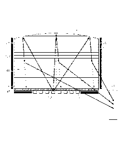
profile and shifting
off normal. However, in other embodiments having silver coated or metallized
extraction
features, the increased angular spread and central normal direction may be
preserved.
Continuing the description of the embodiment with silver coated extraction
features, in the xz
plane, light may exit the stepped waveguide I approximately collimated and may
be directed off
normal in proportion to the y-position of the respective illuminator element
15a ¨ 15n in
illuminator array 15 from the input edge center. Having independent
illuminator elements 15a ¨
15n along the input end 2 then enables light to exit from the entire first
light directing side 6 and
propagate at different external angles, as illustrated in FIGURE 1A.
[00122] Illuminating a spatial light modulator (SLM) 48 such as a fast
liquid crystal
display (LCD) panel with such a device may achieve autostereoscopic 3D as
shown in top view
or yz-plane viewed from the illuminator array 15 end in FIGURE 2A, front view
in FIGURE 2B
and side view in FIGURE 2C. FIGURE 2A is a schematic diagram illustrating in a
top view,
propagation of light in a directional display device, FIGURE 2B is a schematic
diagram
illustrating in a front view, propagation of light in a directional display
device, and FIGURE 2C
is a schematic diagram illustrating in side view propagation of light in a
directional display
device. As illustrated in FIGURES 2A, 2B, and 2C, a stepped waveguide 1 may be
located
behind a fast (e.g., greater than 100Hz) LCD panel SLM 48 that displays
sequential right and left
eye images. In synchronization, specific illuminator elements 15a through 15n
of illuminator
array 15 (where n is an integer greater than one) may be selectively turned on
and off, providing
illuminating light that enters right and left eyes substantially independently
by virtue of the
CA 02871779 2014-10-27
WO 2013/173507 PCMJS2013/041228
21
system's directionality. In the simplest case, sets of illuminator elements of
illuminator array 15
are turned on together, providing a one dimensional viewing window 26 or an
optical pupil with
limited width in the horizontal direction, but extended in the vertical
direction, in which both
eyes horizontally separated may view a left eye image, and another viewing
window 44 in which
a right eye image may primarily be viewed by both eyes, and a central position
in which both the
eyes may view different images. In this way, 3D may be viewed when the head of
a viewer is
approximately centrally aligned. Movement to the side away from the central
position may
result in the scene collapsing onto a 2D image.
[00123] In one embodiment, a stepped waveguide 1 may include an input end 2
which
may be thin and a reflective end 4 which may be thicker than the input end 2.
In one
embodiment the reflective end may have positive optical power. The stepped
waveguide 1 may
also include a first guide surface 6 and a second guide surface 8. The second
guide surface 8 may
include extraction features 10 and guiding features 12. The first guide
surface 6 may be arranged
to guide light by total internal reflection and the second guide surface may
have a plurality of
light extraction features oriented to reflect light guided through the
waveguide in directions
allowing exit through the first guide surface as the output light. The light
extraction features 10
may be facets of the second guide surface. The second guide surface may
include facets and
regions alternating with the facets that may be arranged to direct light
through the waveguide
without substantially extracting it.
[00124] In another embodiment, the first guide surface of another waveguide
may be
arranged to guide light by total internal reflection and the second guide
surface may be
substantially planar and inclined at an angle to reflect light in directions
that break the total
internal reflection for outputting light through the first guide surface. The
display device may
further include a deflection element extending across the first guide surface
of the waveguide for
deflecting light towards the normal to the spatial light modulator. The
reflective end may have
positive optical power.
[00125] The reflective end 4 may have positive optical power in the lateral
direction
across the waveguide. In embodiments in which typically the reflective end 4
has positive optical
power, the optical axis may be defined with reference to the shape of the
reflective end 4, for
example being a line that passes through the center of curvature of the
reflective end 4 and
coincides with the axis of reflective symmetry of the end 4 about the x-axis.
In the case that the
CA 02871779 2014-10-27
WO 2013/173507 PCMJS2013/041228
22
reflecting surface 4 is flat, the optical axis may be similarly defined with
respect to other
components having optical power, for example the light extraction features 12
if they are curved,
or the Fresnel lens 62 described below. The optical axis 238 is typically
coincident with the
mechanical axis of the waveguide 1.In the present embodiments that typically
include a
substantially cylindrical reflecting surface at end 4, the optical axis 238 is
a line that passes
through the center of curvature of the surface at end 4 and coincides with the
axis of reflective
symmetry of the side 4 about the x-axis. The optical axis 238 is typically
coincident with the
mechanical axis of the waveguide 1. The cylindrical reflecting surface at end
4 may typically
include a spherical profile to optimize performance for on-axis and off-axis
viewing positions.
Other profiles may be used.
[00126] FIGURE 3 is a schematic diagram illustrating in side view a
directional display
device. Further, FIGURE 3 illustrates additional detail of a side view of the
operation of a
stepped waveguide 1, which may be a transparent material. The stepped
waveguide 1 may
include an illuminator input end 2, a reflective end 4, a first light
directing side 6 which may be
substantially planar, and a second light directing side 8 which includes
guiding features 10 and
light extraction features 12. In operation, light rays 16 from an illuminator
element 15c of an
illuminator array 15 (not shown in FIGURE 3), that may be an addressable array
of LEDs for
example, may be guided in the stepped waveguide 1 by means of total internal
reflection by the
first light directing side 6 and total internal reflection by the guiding
feature 10, to the reflective
end 4, which may be a mirrored surface. Although reflective end 4 may be a
mirrored surface
and may reflect light, it may in some embodiments also be possible for light
to pass through
reflective end 4.
[00127] Continuing the discussion of FIGURE 3, light ray 18 reflected by
the reflective
end 4 may be further guided in the stepped waveguide 1 by total internal
reflection at the
reflective end 4 and may be reflected by extraction features 12. Light rays 18
that are incident on
extraction features 12 may be substantially deflected away from guiding modes
of the stepped
waveguide 1 and may be directed, as shown by ray 20, through the side 6 to an
optical pupil that
may form a viewing window 26 of an autostereoscopic display. The width of the
viewing
window 26 may be determined by at least the size of the illuminator, output
design distance and
optical power in the side 4 and extraction features 12. The height of the
viewing window may be
primarily determined by the reflection cone angle of the extraction features
12 and the
CA 02871779 2014-10-27
WO 2013/173507 PCMJS2013/041228
23
illumination cone angle input at the input end 2. Thus each viewing window 26
represents a
range of separate output directions with respect to the surface normal
direction of the spatial light
modulator 48 that intersect with a plane at the nominal viewing distance.
[001281 FIGURE 4A is a schematic diagram illustrating in front view a
directional
display device which may be illuminated by a first illuminator element and
including curved
light extraction features. In FIGURE 4A, the directional backlight may include
the stepped
waveguide 1 and the light source illuminator array 15. Further, FIGURE 4A
shows in front
view further guiding of light rays from illuminator element 15c of illuminator
array 15, in the
stepped waveguide 1. Each of the output rays are directed towards the same
viewing window 26
from the respective illuminator 14. Thus light ray 30 may intersect the ray 20
in the window 26,
or may have a different height in the window as shown by ray 32. Additionally,
in various
embodiments, sides 22, 24 of the waveguide 1 may be transparent, mirrored, or
blackened
surfaces. Continuing the discussion of FIGURE 4A, light extraction features 12
may be
elongate, and the orientation of light extraction features 12 in a first
region 34 of the light
directing side 8 (light directing side 8 shown in FIGURE 3, but not shown in
FIGURE 4A) may
be different to the orientation of light extraction features 12 in a second
region 36 of the light
directing side 8.
[00129] FIGURE 4B is a schematic diagram illustrating in front view a
directional
display device which may illuminated by a second illuminator element. Further,
FIGURE 4B
shows the light rays 40, 42 from a second illuminator element 15h of the
illuminator array 15.
The curvature of the reflective surface on the side 4 and the light extraction
features 12
cooperatively produce a second viewing window 44 laterally separated from the
viewing window
26 with light rays from the illuminator element 15h.
[00130] Advantageously, the arrangement illustrated in FIGURE 4B may
provide a real
image of the illuminator element 15c at a viewing window 26 in which the real
image may be
formed by cooperation of optical power in reflective end 4 and optical power
which may arise
from different orientations of elongate light extraction features 12 between
regions 34 and 36, as
shown in FIGURE 4A. The arrangement of FIGURE 4B may achieve improved
aberrations of
the imaging of illuminator element 15c to lateral positions in viewing window
26. Improved
aberrations may achieve an extended viewing freedom for an autostereoscopic
display while
achieving low cross talk levels.
CA 02871779 2014-10-27
WO 2013/173507 PCMJS2013/041228
24
[00131] FIGURE 5 is a schematic diagram illustrating in front view an
embodiment of a
directional display device including a waveguide 1 having substantially linear
light extraction
features. Further, FIGURE 5 shows a similar arrangement of components to
FIGURE 1 (with
corresponding elements being similar), with one of the differences being that
the light extraction
features 12 are substantially linear and parallel to each other.
Advantageously, such an
arrangement may provide substantially uniform illumination across a display
surface and may be
more convenient to manufacture than the curved extraction features of FIGURE
4A and
FIGURE 4B.
[00132] FIGURE 6A is a schematic diagram illustrating one embodiment of the
generation of a first viewing window in a time multiplexed imaging directional
display device in
a first time slot, FIGURE 6B is a schematic diagram illustrating another
embodiment of the
generation of a second viewing window in a time multiplexed imaging
directional backlight
apparatus in a second time slot, and FIGURE 6C is a schematic diagram
illustrating another
embodiment of the generation of a first and a second viewing window in a time
multiplexed
imaging directional display device. Further, FIGURE 6A shows schematically the
generation of
illumination window 26 from stepped waveguide 1. Illuminator element group 31
in illuminator
array 15 may provide a light cone 17 directed towards a viewing window 26.
FIGURE 6B
shows schematically the generation of illumination window 44. Illuminator
element group 33 in
illuminator array 15 may provide a light cone 19 directed towards viewing
window 44. In
cooperation with a time multiplexed display, windows 26 and 44 may be provided
in sequence as
shown in FIGURE 6C. If the image on a spatial light modulator 48 (not shown in
FIGURES 6A,
6B, 6C) is adjusted in correspondence with the light direction output, then an
autostereoscopic
image may be achieved for a suitably placed viewer. Similar operation can be
achieved with all
the directional backlights and directional display devices described herein.
Note that illuminator
element groups 31, 33 each include one or more illumination elements from
illumination
elements 15a to 15n, where n is an integer greater than one.
[00133] FIGURE 7 is a schematic diagram illustrating one embodiment of an
observer
tracking autostereoscopic directional display device including a time
multiplexed directional
backlight. As shown in FIGURE 7, selectively turning on and off illuminator
elements 15a to
15n along axis 29 provides for directional control of viewing windows. The
head 45 position
may be monitored with a camera, motion sensor, motion detector, or any other
appropriate
CA 02871779 2014-10-27
WO 2013/173507 PCMJS2013/041228
optical, mechanical or electrical means, and the appropriate illuminator
elements of illuminator
array 15 may be turned on and off to provide substantially independent images
to each eye
irrespective of the head 45 position. The head tracking system (or a second
head tracking
system) may provide monitoring of more than one head 45, 47 (head 47 not shown
in FIGURE
7) and may supply the same left and right eye images to each viewers' left and
right eyes
providing 3D to all viewers. Again similar operation can be achieved with all
the directional
backlights and directional display devices described herein.
[00134] FIGURE 8 is a schematic diagram illustrating one embodiment of a
multi-viewer
directional display device as an example including an imaging directional
backlight. As shown
in FIGURE 8, at least two 2D images may be directed towards a pair of viewers
45, 47 so that
each viewer may watch a different image on the spatial light modulator 48. The
two 2D images
of FIGURE 8 may be generated in a similar manner as described with respect to
FIGURE 7 in
that the two images would be displayed in sequence and in synchronization with
sources whose
light is directed toward the two viewers. One image is presented on the
spatial light modulator 48
in a first phase, and a second image is presented on the spatial light
modulator 48 in a second
phase different from the first phase. In correspondence with the first and
second phases, the
output illumination is adjusted to provide first and second viewing windows
26, 44 respectively.
An observer with both eyes in window 26 will perceive a first image while an
observer with both
eyes in window 44 will perceive a second image.
[00135] FIGURE 9 is a schematic diagram illustrating a privacy directional
display
device which includes an imaging directional backlight apparatus. 2D display
systems may also
utilize directional backlighting for security and efficiency purposes in which
light may be
primarily directed at the eyes of a first viewer 45 as shown in FIGURE 9.
Further, as illustrated
in FIGURE 9, although first viewer 45 may be able to view an image on device
50, light is not
directed towards second viewer 47. Thus second viewer 47 is prevented from
viewing an image
on device 50. Each of the embodiments of the present disclosure may
advantageously provide
autostereoscopic, dual image or privacy display functions.
[00136] FIGURE 10 is a schematic diagram illustrating in side view the
structure of a
time multiplexed directional display device as an example including an imaging
directional
backlight. Further, FIGURE 10 shows in side view an autostereoscopic
directional display
device, which may include the stepped waveguide 1 and a Fresnel lens 62
arranged to provide
the viewing window 26 for a substantially collimated output across the stepped
waveguide 1 output
surface. A vertical diffuser 68 may be arranged to extend the height of the
window 26 further. The
light may then be imaged through the spatial light modulator 48. The
illuminator array 15 may include
light emitting diodes (LEDs) that may, for example, be phosphor converted blue
LEDs, or may be
separate RGB LEDs. Alternatively, the illuminator elements in illuminator
array 15 may include a
uniform light source and spatial light modulator arranged to provide separate
illumination regions.
Alternatively the illuminator elements may include laser light source(s). The
laser output may be
directed onto a diffuser by means of scanning, for example, using a galvo or
MEMS scanner. In one
example, laser light may thus be used to provide the appropriate illuminator
elements in illuminator
array 15 to provide a substantially uniform light source with the appropriate
output angle, and further
to provide reduction in speckle. Alternatively, the illuminator array 15 may
be an array of laser light
generating elements. Additionally in one example, the diffuser may be a
wavelength converting
phosphor, so that illumination may be at a different wavelength to the visible
output light.
[00137] FIGURE HA is a schematic diagram illustrating a front view of another
imaging directional
backlight apparatus, as illustrated, a wedge type directional backlight, and
FIGURE 11B is a schematic
diagram illustrating a side view of the same wedge type directional backlight
apparatus. The structure
may include a wedge type waveguide 1104 with a bottom surface which may be
preferentially coated
with a reflecting layer 1106 and with an end corrugated surface 1102, which
may also be preferentially
coated with a reflecting layer 1106. As shown in FIGURE 11B, light may enter
the wedge type
waveguide 1104 from local sources 1101 and the light may propagate in a first
direction before
reflecting off the end surface. Light may exit the wedge type waveguide 1104
while on its return path
and may illuminate a display panel 1110. By way of comparison with a stepped
waveguide, a wedge
type waveguide provides extraction by a taper that reduces the incidence angle
of propagating light so
that when the light is incident at the critical angle on an output surface, it
may escape. Escaping light
at the critical angle in the wedge type waveguide propagates substantially
parallel to the surface until
deflected by a redirection layer 1108 such as a prism array. Errors or dust on
the wedge type waveguide
output surface may change the critical angle, creating stray light and
uniformity errors. Further,
26
Date Re9ue/Date Received 2020-09-08
CA 02871779 2014-10-27
WO 2013/173507 PCMJS2013/041228
27
an imaging directional backlight that uses a mirror to fold the beam path in
the wedge type
directional backlight may employ a faceted mirror that biases the light cone
directions in the
wedge type waveguide. Such faceted mirrors are generally complex to fabricate
and may result
in illumination uniformity errors as well as stray light.
[00138] The wedge type waveguide and stepped waveguide further process
light beams in
different ways. In the wedge type waveguide, light input at an appropriate
angle will output at a
defined position on a major surface, but light rays will exit at substantially
the same angle and
substantially parallel to the major surface. By comparison, light input to a
stepped waveguide at
a certain angle may output from points across the first side, with output
angle determined by
input angle. Advantageously, the stepped waveguide may not require further
light re-direction
films to extract light towards an observer and angular non-uniformities of
input may not provide
non-uniformities across the display surface.
[00139] Continuing the discussion of FIGURE 10, a vertical diffuser 68 may
be arranged
to further extend the height of the window 26. The light may then be imaged
through the spatial
light modulator 48 to an observer at or near to the window 26.
[00140] Continuing the discussion of FIGURE 10, the stepped waveguide I may
include
an input end 2 which may be thin and a reflective end 4 which may be thicker
than the input end
2. In one embodiment the reflective end may have positive optical power. The
stepped
waveguide 1 may also include a first guide surface 6 and a second guide
surface 8. The second
guide surface 8 may include extraction features 10 and guiding features 12.
The first guide
surface 6 may be arranged to guide light by total internal reflection and the
second guide surface
may have a plurality of light extraction features oriented to reflect light
guided through the
waveguide in directions allowing exit through the first guide surface as the
output light. The
light extraction features 10 may be facets of the second guide surface. The
second guide surface
may include facets and regions alternating with the facets that may be
arranged to direct light
through the waveguide without substantially extracting it.
[00141] In another embodiment, the first guide surface of another waveguide
may be
arranged to guide light by total internal reflection and the second guide
surface may be
substantially planar and inclined at an angle to reflect light in directions
that break the total
internal reflection for outputting light through the first guide surface. The
display device may
further include a deflection element extending across the first guide surface
of the waveguide for
CA 02871779 2014-10-27
WO 2013/173507 PCMJS2013/041228
28
deflecting light towards the normal to the spatial light modulator. The
reflective end may have
positive optical power.
[00142] In another embodiment a display device may include a directional
backlight and a
transmissive spatial light modulator. The transmissive spatial light modulator
may be arranged
to receive the output light from the directional backlight. The transmissive
spatial light
modulator may include an array of pixels arranged to modulate light passing
therethrough.
[00143] There will now be described some waveguides, directional backlights
and
directional display devices that are based on and incorporate the structures
of FIGURES 1 to 10
above. Except for the modifications and/or additional features which will now
be described, the
above description applies equally to the following waveguides, directional
backlights and display
devices, but for brevity will not be repeated. The waveguides described below
may be
incorporated into a directional backlight or a directional display device as
described above.
Similarly, the directional backlights described below may be incorporated into
a directional
display device as described above.
[00144] FIGURE 12 is a schematic diagram illustrating a directional display
apparatus
including a display device 100 and a control system. The arrangement and
operation of the
control system will now be described and may be applied, with changes as
necessary, to each of
the display devices disclosed herein.
[00145] The waveguide 1 is arranged as described above. The reflective end
4 converges
the reflected light. A Fresnel lens 62 may be arranged to cooperate with
reflective end 4 to
achieve viewing windows 26 at a viewing plane 106 observed by an observer 99.
A transmissive
spatial light modulator (SLM) 48 may be arranged to receive the light from the
directional
backlight. Further a diffuser 68 may be provided to substantially remove Moire
beating between
the waveguide 1 and pixels of the SLM 48 as well as the Fresnel lens 62.
[00146] The control system may include a sensor system arranged to detect
the position of
the observer 99 relative to the display device 100. The sensor system includes
a position sensor
70, such as a camera, and a head position measurement system 72 that may for
example include
a computer vision image processing system. The control system may further
include an
illumination controller 74 and an image controller 76 that are both supplied
with the detected
position of the observer supplied from the head position measurement system
72.
CA 02871779 2014-10-27
WO 2013/173507 PCMJS2013/041228
29
[00147] The illumination controller 74 selectively operates the illuminator
elements 15 to
direct light to into the viewing windows 26 in cooperation with waveguide 1.
The illumination
controller 74 selects the illuminator elements 15 to be operated in dependence
on the position of
the observer detected by the head position measurement system 72, so that the
viewing windows
26 into which light is directed are in positions corresponding to the left and
right eyes of the
observer 99. In this manner, the lateral output directionality of the
waveguide 1 corresponds with
the observer position.
[00148] The image controller 76 controls the SLM 48 to display images. To
provide an
autostereoscopic display, the image controller 76 and the illumination
controller 74 may operate
as follows. The image controller 76 controls the SLM 48 to display temporally
multiplexed left
and right eye images. The illumination controller 74 operate the light sources
15 to direct light
into viewing windows in positions corresponding to the left and right eyes of
an observer
synchronously with the display of left and right eye images. In this manner,
an autostereoscopic
effect is achieved using a time division multiplexing technique.
[00149] FIGURE 13 is a schematic diagram illustrating generation of viewing
windows
from a discontinuous array of illuminator elements. Further, FIGURE 13 shows
the imaging of a
illuminator element array 15 including, for example, discrete illuminator
elements 100,102
which may be separated by gap 101. Light propagating through the stepped
waveguide 1 that is
imaged by mirror on surface 4 and light extraction features 12 may be imaged
towards a set of
windows with window 26 being an image of illuminator 100 and window 27 being
an image of
illuminator 27. Gap 101 may be effectively imaged to a gap 29. In this
embodiment, the
imaging function of the light guide may be substantially one dimensional, so
the vertical height
of the illuminators may be extended. In operation gaps 29 may provide image
flicker and non-
uniform display intensity for an observer and are thus undesirable.
[00150] FIGURE 14 is a schematic diagram illustrating generation of viewing
windows
from a discontinuous array of illuminator elements. Further, FIGURE 14 shows
that a diffuser 68
may be arranged so that the width of the windows 26, 27 is increased and gap
29 (as shown in
FIGURE 14) reduced. Typically in an approximately 17" screen diagonal size
display viewed
from an approximate distance of 500mm, the diffuser 68 may be an asymmetric
diffuser with, for
example, a diffusion angle of approximately 30 degrees in the vertical
direction and
approximately 3 degrees in the horizontal direction. For large displays of
approximate size 40"
CA 02871779 2014-10-27
WO 2013/173507 PCMJS2013/041228
screen diagonal size viewed from an approximate distance of 3m, the diffuser
may achieve a
smaller lateral diffusion angle, for example, approximately 1 degree to reduce
cross talk leakage
between adjacent eyes. Advantageously, an asymmetric diffuser may be used to
provide blurring
between images of the illuminator elements in the window plane arising from
discrete
illuminator elements, while maintaining low cross talk.
[00151] FIGURE 15 is a schematic diagram illustrating an origin of stray
light in a
waveguide 1. Further, FIGURE 15 shows illumination by a directional backlight
of a viewing
window 26 as described in FIGURE 5. However, stray light rays 104 that may not
be incident
on light extraction features 12 during propagation in the stepped waveguide
after incidence on
mirror surface 4 may be incident onto surface 2. In other words, the
individual illuminator
elements 100, 102 of the illuminator array 15 may return a certain proportion
of light to the input
end 2.
[00152] FIGURE 16 is a schematic diagram illustrating generation of
secondary viewing
windows from stray light in a waveguide 1. Further, FIGURE 16 shows the
propagation of the
stray light rays 104 after incidence on surface 2. Light rays 104 that were
directed from
illuminator element 100 thus may fall onto the illuminator element 102. The
structure of
illuminator element 102 may reflect light in a diffuse manner back into the
stepped waveguide 1
as shown for example by ray 106. After reflection at mirror surface 4, light
ray 108 may be
incident on a light extraction feature 12 of the stepped waveguide 1 and be
extracted towards the
window plane. As the light was imaged from position of illuminator element
102, it may be
directed to a stray light window 110. Thus light that was intended for
illumination of window 26
may become incident on a different window 110. If the illuminator element 100
corresponds to a
right eye 114 illumination and illuminator element 102 corresponds to a left
eye 116 illumination
then such a process may image right eye data into the left eye 116 of an
observer 112, creating
undesirable cross-talk that degrades 3D autostereoscopic image quality.
[00153] In addition to reflection from the illuminator elements of the
illuminator array 15
of FIGURE 17, light may also be reflected in a specular manner by the input
end 2, when surface
of the input end 2 is substantially flat as illustrated in FIGURE 17. FIGURE
17 is a schematic
diagram illustrating a further illumination artifact arising from stray light
in a waveguide 1. Light
rays 104 may be specularly reflected at surface 2 to provide rays 120. The
rays 120 may be
reflected at surface 4 to provide rays 122. Such a '4 pass' artifact may
result in extraction at
CA 02871779 2014-10-27
WO 2013/173507 PCMJS2013/041228
31
features 12 along rays 123 towards window 26 such that ray 122 may be seen as
a single line on
the display surface for an observer in window 26 when illuminated by a
illuminator element 100.
It would thus be desirable to remove stray light rays 122, and thus output
rays 123, to reduce the
4-pass artifact. Additionally, it may be desirable to reduce the visibility of
image cross talk and
4-pass artifacts, thus increasing the performance of the display.
[00154] FIGURE 18 is a schematic diagram illustrating a directional
backlight arranged
to reduce stray light propagation. Further, FIGURE 18 shows an embodiment of a
directional
backlight including a waveguide 1 arranged as described above but with a low
reflectivity input
end 2.
[00155] Stepped waveguide 1 may include a low reflection layer 124 that may
be arranged
at the surface of the input end 2, for example, by means of bonding with an
adhesive. The low
reflection layer 124 acts as a reflection reduction element arranged to reduce
reflections of light
incident on the input end 2 after reflection from the reflective end 4. The
layer 124 may include
at least one reflection reducing element as will be described, for example, in
FIGURE 19 below.
The low reflection layer 124 extends across the entirety of the input end 2.
[00156] In addition, light absorbing elements 126 may be arranged to absorb
light rays
104 from the valve. The light absorbing elements 126 further act as a
reflection reduction
element arranged to reduce reflections of light incident on the input end 2
after reflection from
the reflective end 4 and may include a light absorptive layer. The light
absorbing elements 126
may extend across part of the input end 2 of the waveguide 1, outside of the
illuminator elements
100. As illustrated in FIGURE 18, the light rays 104 may originate from an
illuminator element
100 of the illuminator array 115. The light absorbing elements 126 may include
for example a
black absorbing layer arranged in the regions not occupied by the illuminator
elements 100 of the
illuminator array 15. By absorbing stray light incident on the input end 2,
the light absorbing
elements 126 reduce artifacts of the type described above with reference to
FIGURE 17.
[00157] Further light absorbing elements 127 may be arranged along the
surfaces or sides
22, 24 of the waveguide 1 to absorb incident stray light. Absorbing elements
126, 127 may be,
for example, dyes, pigments contained in paints, adhesive films, and so forth.
[00158] In the present disclosure an optical window refers to the image of
a single light
source in the window plane. By way of comparison, a viewing window 26 is the
region in the
window plane wherein light is provided including image data of substantially
the same image
CA 02871779 2014-10-27
WO 2013/173507 PCMJS2013/041228
32
from across the display area. Thus a viewing window 26 may be formed from
multiple optical
windows.
[00159] FIGURE 19 is a schematic diagram illustrating one embodiment of a
directional
backlight including a stray light reduction arrangement. Further, FIGURE 19
shows a detail of an
example of low reflection layers 124. The directional backlight includes a
waveguide 1 arranged
as described above but with a low reflectivity input end 2. In particular, the
waveguide 1 may
include a low reflection layer 124 as described above with reference to FIGURE
18. The low
reflection layer 124 acts as a reflection reduction element and is arranged to
reduce reflections of
light incident on the input end after reflection from the reflective end., and
is arranged as
follows.
[00160] The waveguide 1 of FIGURE 19 may include an input end 2 which may
be
operable to receive light from the illumination array 15. The low reflection
layer 124 may be
located between the input end 2 and the illumination array 15. Input light
rays 16 may be
provided by illuminator elements 100 of the illuminator array 15. There will
now be described
the arrangement of the illuminator elements 100 which may be applied in any of
the directional
backlights and directional di splay devices described herein.
[00161] Illuminator elements 100 of the illuminator array 15 may include
multiple
illuminator elements 140. As illustrated in FIGURE 21, adjacent elements 140
may be used as a
single illuminator element 102. In one example, the elements 140 may be LEDs
(light emitting
diodes). Illuminator elements 140 may include at least a package body 142, an
emitting chip 144
and wire bonds 146, and phosphor 148. The package body 142 acts as a substrate
and the
emitting chip 144 and the phosphor 148 are supported thereon.
[00162] The emitting chip 144 may act as a light generation element which
is arranged to
generate light in an emission band, for example blue light. The phosphor 148
acts a wavelength
conversion material which is arranged to convert light in the emission band
generated by the
light generation element into light in a conversion band, for example yellow
light. In one
example, the emitting chip 144 may be a semiconductor diode
[00163] FIGURE 23 is a schematic diagram illustrating a graph of a typical
white spectral
distribution of a light source, that might be that of an illuminator element
140 or any of the light
sources described herein. Output radiance 400 is plotted against wavelength in
nanometers for
an illustrative light source including an emission band including the
distribution 404 and
CA 02871779 2014-10-27
WO 2013/173507 PCMJS2013/041228
33
conversion band including the distribution 406. The emission band may
alternatively be
considered to be the spectral region 408 and the conversion band may be
considered to be the
spectral region 410. Thus an array 15 of light sources may be arranged to
output light
predominantly in an emission band and in a conversion band. Advantageously
such sources may
achieve high output luminous efficiency with white points and spectral
distributions for
illumination of spatial light modulators 48 to achieve desirable color
characteristics of displayed
images.
[00164] Continuing the discussion of FIGURE 19, the low reflection layer
124 may
include a layer 128 which is a filter. The layer 128 is disposed between the
input end 2 and the
illuminator elements 100, although in this example the layer 128 further
extends across the
entirety of the input end 2. Incident stray light 104 is incident on the layer
128 which may be an
absorption color filter which may be arranged to absorb light in the
conversion band
preferentially over light in the emission band. In that case the layer 128
preferentially transmits a
greater portion of light in the emission band than light in the conversion
band.
[00165] For example, layer 128 may include color filters such as 'Surprise
Pink' supplied
by Roscoe Laboratories Inc. 1265 Los Angeles Street, Glendale, CA, USA, 91204,
with a
percentage transmission 137 as shown as a function of incident wavelength 139
by FIGURE 20.
Color filter 128 may additionally or alternatively include at least one
quantum dot material.
Advantageously quantum dots can achieve optical properties that are determined
from their
physical size rather than chemical make-up so that absorption bands can be
controlled by means
of modifying the physical size of the light absorbing particles. Such
particles may be arranged in
a layer with a substantially transparent binding material.
[00166] The low reflection layer 124 may further include a secondary layer
130 which
may be a film with an anti-reflection coating 132.
[00167] FIGURE 20 is a schematic diagram illustrating the transmission
spectrum of one
example of a color absorption filter used in the low reflection layer 124 of
FIGURE 19. The low
reflection layer 124 may be arranged as one or more films that may be attached
to the surface of
the input end 2 of the stepped waveguide 1 by means of pressure sensitive
adhesive layers or by
other known attachment methods.
[00168] On incidence with layer 128, light ray 104 may be partially
absorbed in the color
filter. This light may be incident on the phosphor 148 of an illuminator
element 140 arranged as
CA 02871779 2014-10-27
WO 2013/173507 PCMJS2013/041228
34
described above. A portion of incident light in the emission band in ray 134
may be absorbed by
the phosphor 148 so that light rays 136 may be scattered by the phosphor and
reflected by the
package body 142 and the emitting chip 144. Thus the reflected light ray 136
from the element
140 may have a color that has a lower intensity in the emission band than the
incident light ray
134. Light ray 136 is one example of a typically diffuse light cone. On
incidence with the layer
128, light ray 136 may be preferentially absorbed in the conversion band of
the spectrum. Stated
differently, the ray 136 may have a greater intensity in the conversion band
than light ray 104,
thus the reflection may be preferentially absorbed.
[00169] Continuing the discussion of FIGURES 19 and 20, light rays may be
directly
emitted from the chip 144 and may undergo a single pass through the filter
128, whereas the
stray light 104 may undergo a double pass to provide ray 138 with a
substantially reduced
relative intensity. Thus while the filter of layer 128 may degrade overall
efficiency,
advantageously it may increase the color temperature of illumination of light
rays 16 from the
emitting chip 144 and phosphor 148. Illumination of color filter LCD panels
may typically
benefit from a high color temperature, as advantageously a greater color gamut
may be produced.
[00170] In an alternative embodiment, layer 128 may be a grey absorbing
filter with an
approximate transmission of 80%, so that the stray light 104 may undergo a
double pass, thus
giving an approximately 64% transmission. Additionally, the input light 16 may
undergo a
single pass, with an approximately 80% transmission, thus reducing the
visibility of the stray
light.
[00171] Layer 132 may provide a low reflectivity interface between the
stepped
waveguide and air which may be provided by dielectric coatings or other known
anti-reflection
coatings such as moth-eye surfaces. Advantageously, the elements 140 may be
arranged in air so
that the Lambertian light cone in air may be reduced to an angle of twice the
critical angle in the
material of the stepped waveguide. Advantageously such an arrangement may be
provided to
achieve efficient illumination of the mirror surface 4. Further, such an
arrangement may reduce
the amount of stray light that may be incident on to the sides 22, 24 of the
stepped waveguide,
thus reducing the total amount of stray light in the system. Advantageously
the present
embodiments may reduce image cross talk and may reduce the visibility of stray
light artifacts
while achieving efficient illumination of the mirror surface 4.
CA 02871779 2014-10-27
WO 2013/173507 PCMJS2013/041228
[00172] FIGURE 21 is a schematic diagram illustrating a detail of a further
directional
backlight including a stray light reduction arrangement that may be used in
place of, in addition
to, and/or in combination with layer 124 of FIGURE 19.
[00173] In FIGURE 21 a substrate 131 may be arranged with an array of light
modulating
structures 129 that act as a reflection reduction element arranged to reduce
reflections of light
incident on the input end 2 after reflection from the reflective end 4. In one
example, the
substrate 131 may be the layer 128 of FIGURE 19.
[00174] Returning to the discussion of FIGURE 21, each light modulating
structure 129
covers part of the area of the illuminator element 140 which is arranged as
described above. In
this example, each respective illuminator element has plural light modulating
structure 129
covering part of its area with gaps in between, but in general each respective
illuminator element
has plural light modulating structure 129 may have any number of one or more
light modulating
structures 129 covering part of its area.
[00175] Each light modulating structure 129 may include a light absorbing
layer 133 and a
light reflecting layer 135. The light absorbing layer 133 faces the waveguide
1 and the light
reflecting layer 135 faces the illuminator element 140. Incident stray light
104 may be absorbed
on the absorbing layer 133 while light that is emitted by illuminator elements
144 of the
illuminator array 15 may be transmitted through gaps between the light
modulating structures
129. Due to the absorption by the absorbing layer 133, the light modulating
structures 129 act as
light absorbing elements that absorb light after reflection from the
reflective end 4.
[00176] Light that is incident on the layer 135 of light modulating
structures 129 may be
substantially reflected back towards the illuminator elements 144 and the
light may be
substantially reflected and/or scattered back towards the gaps between the
light modulating
structures 129, for output into the stepped waveguide 1. Advantageously such
an arrangement
may achieve reduction in stray light reflection into the stepped waveguide 1
by means of
absorption at layer 133, while achieving high output efficiency due to
recycling of light by the
reflective layer 135.
[00177] FIGURE 22 is a schematic diagram illustrating an end view of the
directional
backlight of FIGURE 21 illustrating the coverage of the light modulating
elements 129 over the
illuminator element 140. Light modulating elements 129 may be arranged with
respect to the
illuminator elements to improve output uniformity across the illuminator array
15 of illuminator
CA 02871779 2014-10-27
WO 2013/173507 PCMJS2013/041228
36
elements. Thus, the reflectors may be positioned near the chip 144 and may be
arranged to
reflect light in the emission band more widely onto the phosphor 148. Further,
some controlled
mixing may be achieved between adjacent illuminator elements, while reducing
stray light
reflection. Advantageously the window plane uniformity may be improved, and
the color
variation across the window plane may be reduced. Light control elements may
be formed, for
example, by selective etching of a mirror which may include a first absorbing
layer 133 and a
reflective layer 135. Alternatively, reflective and absorbing inks may be
printed in approximate
registration onto a substrate. The reflective layer 135 may be metallic, for
example, or may be a
diffuse white reflective layer.
[00178] FIGURE 24 is a schematic diagram illustrating a further directional
backlight
including a stray light reduction arrangement. A spatial light modulator 150
such as a liquid
crystal shutter may be arranged between the illuminator elements 100, 102 and
the input end 2 of
the stepped waveguide 1. The spatial light modulator 150 acts a reflection
reduction element
arranged to reduce reflections of light incident on the input end 2 after
reflection from the
reflective end 4, as follows.
[00179] The spatial light modulator 150 covers at least the illuminator
elements 100, in
this example extending across the entirety of the input end 2. The spatial
light modulator 150
acts as a shutter and may be a liquid crystal shutter including a switchable
liquid crystal layer
156 which may include addressable pixel regions 162, 164, substrates 154, 158,
such as glass
substrates and optional polarizers 152, 160 such as stretched PVA with iodine
preferential
absorber, reflective polarizer such as DBEF from 3M Corporation, wire grid
polarizers or
combination therein. The liquid crystal mode may be, but is not limited to,
twisted nematic,
super-twisted nematic, guest host, ferroelectric, or any other known modes.
The modulator 150
may be proximate to or attached to the surface of the input end 2, to the
illuminator array 15 or
may be in air. Additional absorption filters 128 and anti-reflective coatings
132 may be arranged
as appropriate. Thus, the spatial light modulator 150 acts as a shutter that
may be operable so that
portions of the spatial light modulator 150 adjacent respective illuminator
elements 100
selectively transmit light when the respective illuminator elements 100 is
operated and otherwise
absorb light incident on the input end 2 after reflection from the reflective
end 4.
[00180] Further, the elements 100, 102 may be replaced by a continuous
illuminator
element wherein the shutter 150 acts to achieve the illuminator element array
15. However, such
CA 02871779 2014-10-27
WO 2013/173507 PCMJS2013/041228
37
an element may not achieve as high extinction properties as the embodiment of
FIGURE 24
wherein the illuminator elements are individually controllable.
[00181] As illustrated in FIGURE 24, light may be emitted from illuminator
element 100
and pass through the transmissive region of pixels 162. The light may be
reflected from the
reflective end 4 and the stray light rays 104 may, at least in part, be
directed towards non-
illuminated elements 102 and substantially absorbed.
[00182] FIGURE 25 is a schematic diagram illustrating a detail of the
further directional
backlight of FIGURE 24 in one optional construction. . In operation, pixels
162 of the spatial
light modulator 150 in the region of the illuminator elements 100 may be
arranged to be
transmissive whereas pixels 164 in the region of non-illuminated illuminator
elements 100 may
be absorbing to incident light. Thus input rays 16 may be transmitted into the
stepped
waveguide 1 whereas stray light rays 104 may be directed generally towards non-
illuminated
illuminator elements 102 and may be absorbed. In this manner, a dynamic filter
can be arranged
to cooperate with the illumination of the illuminator elements 100, 102 to
advantageously reduce
cross talk and other stray light artifacts. Further, the response speed of the
spatial light
modulator may not match the switching response of the illuminator elements,
but may be similar
to that used in the respective time multiplexed display spatial light
modulator.
[00183] Continuing the discussion of FIGURE 25, the pixels 164 may be
arranged to be
absorbing for most to all respective aligned illuminator elements other than
those for the specific
window to be illuminated. Alternatively the pixels may be absorbing in the
region of the
illuminator array 15 that may result in cross talk to the observer's eye, for
example, the
illuminator elements that are illuminated in the opposite phase for a given
observer position.
Advantageously, illuminator elements that are not directed to an observer's
eyes can remain
illuminated, so that a multi-viewer display in which multiple groups of
illuminator elements are
illuminated can be provided with low cross talk.
[00184] FIGURE 26 is a schematic diagram illustrating a detail of a further
directional
backlight including a stray light reduction arrangement. Further, FIGURE 26
shows an
embodiment including a saturable absorber 166 which may be formed on support
substrate 168.
The saturable absorber 166 acts a reflection reduction element arranged to
reduce reflections of
light incident on the input end 2 after reflection from the reflective end 4,
as follows.
CA 02871779 2014-10-27
WO 2013/173507 PCMJS2013/041228
38
[00185] The saturable absorber 166 covers at least the illuminator elements
100, in this
example extending across the entirety of the input end 2. In FIGURE 26, the
waveguide 1 may
receive light rays 16 from the illuminator element 100 of the illumination
array 15 at the input
end 2, through the region 172. Illuminator element 100 of the illuminator
array 15 may include
element 140. As illustrated in FIGURE 26, adjacent elements 140 may be used
for illuminator
element 102. In one example, the elements 140 may be LEDs.
[00186] In operation, the light intensity of the illuminator element 100
may be
substantially higher than the intensity of the returning stray light. Thus in
the region 172, the
absorber 166 may saturate and become transmitting whereas in region 170 the
illuminated
intensity may be much lower, and the absorber may be absorbing. As illustrated
in FIGURE 26,
ray 104 may be directed toward region 170, which may substantially absorb the
light ray 104.
Although the absorber 166 as illustrated has a region 170 and a region 172,
the absorber is a
layer of material. The region 172 is represented as such for purposes of
description and to
illustrate that the absorber may become saturated with light in regions and
transmit light through
the saturated region of absorber 166. Thus, the saturable absorber 166 may be
operable so that
portions of the saturable absorber 166 adjacent respective illuminator
elements 100 selectively
transmit light when the respective illuminator elements 100 is operated and
otherwise absorb
light incident on the input end 2 after reflection from the reflective end 4.
[00187] Suitable properties of the saturable absorber 166 are as follows.
Saturable
absorbers may. for example, be phosphor materials. The relaxation time of the
material may be
set to be less than the frame rate of the time multiplexed display spatial
light modulator.
Advantageously such an arrangement may have a less complex construction than a
liquid crystal
spatial light modulator.
[00188] FIGURE 27 is a schematic diagram illustrating a directional
backlight arranged
to reduce stray light propagation. Further, FIGURE 27 shows an embodiment of a
directional
backlight including a waveguide 1, a linear polarizer 174 arranged at the
surface of the input end
2 of the stepped waveguide 1, and a quarter waveplate 176 and a mirror be
arranged at the output
surface of the reflective end 4 between the guiding portion of the waveguide 1
and reflective end
4. The linear polarizer 174 acts a reflection reduction element arranged to
reduce reflections of
light incident on the input end 2 after reflection from the reflective end 4,
as follows.
CA 02871779 2014-10-27
WO 2013/173507 PCMJS2013/041228
39
[00189] Incident light from the illuminator element 100 may be polarized
for transmission
through an input path of the waveguide 1. The quarter waveplate acts as a
phase retarder so that,
at the quarter waveplate 176 and mirror surface of the reflective end 4, the
polarization may be
rotated through approximately 90 degrees so that the opposite polarization
state may counter-
propagate in the stepped waveguide 1. On incidence at the linear polarizer
174, the counter-
propagating stray light rays 104 may thus be absorbed. Advantageously such an
arrangement
may propagate linear polarization states within the waveguide 1 so that
depolarization during
TIR at side 6 and features 10 may be minimized (side 6 and features 10 not
shown in FIGURE
27).
[00190] As illustrated in FIGURE 27, light may be emitted from illuminator
element 100
and pass through the input end 2. The light may be reflected from the
reflective end 4 and the
stray light rays 104 may, at least in part, be substantially absorbed as
previously described. The
reflected light may also be directed towards a viewing window 26.
[00191] FIGURE 28 is a schematic diagram illustrating a directional
backlight arranged
to reduce stray light propagation including a diffusing element, and including
a waveguide 1.
Further, FIGURE 28 shows an embodiment including a surface relief diffusing
surface 188 that
is attached to the surface of the input end 2 of the stepped waveguide 1 by
means of pressure
sensitive adhesive layers or by other known attachment methods. The surface
relief diffusing
surface 188 may extend across the entirety of the input end 2. The surface
relief diffusing surface
188 is an example of a light diffusing element and acts a reflection reduction
element arranged to
reduce reflections of light incident on the input end 2 after reflection from
the reflective end 4, as
follows.
[00192] As illustrated in FIGURE 28, the waveguide 1 may receive light from
a
illumination array 15. More specifically, illuminator element 100 of the
illumination array 15
may input light into the input end of the waveguide 1, and the light may
reflect off of the
reflective end 4 of the waveguide 1. After the light reflects off of the
reflective end 4 of the
waveguide 1, it may travel in the general direction of the diffusing surface
188. At least some of
the light may pass through the diffusing surface 188. As illustrated in FIGURE
28, the rays 20
may exit generally in the direction of the window 26. Light rays 104 may be
incident on to the
diffuser 188 and may be scattered over a wide cone angle. Similarly and as
shown in FIGURE
17, the specular reflection ray 120 of FIGURE 17 may be distributed over a
wide cone angle, so
CA 02871779 2014-10-27
WO 2013/173507 PCMJS2013/041228
that the intensity of light in beams 123 may be reduced. Advantageously the
artifact of rays 123
may be minimized.
[00193] The diffusing surface 188 may have asymmetric diffusing properties.
These
properties may increase the output illumination angular spread in
substantially a first direction in
the plane of the waveguide 1, but provide low diffusion in a plane out of the
waveguide 1, to
reduce light losses from diffusion in this direction.
[00194]
[00195] Alternatively, the diffusing surface 188 of FIGURE 28 may be
replaced by a bulk
diffuser 190 as shown in FIGURE 29, which may further incorporate further
cross talk reduction
embodiments as described elsewhere. FIGURE 29 is a schematic diagram
illustrating a
directional backlight arranged to reduce stray light propagation, including a
waveguide and a
bulk diffuser 190 extending across the input end 2 of the waveguide 1. The
surface relief
diffusing surface 188 is another example of a light diffusing element, and has
the same properties
as the diffusing surface 188 as discussed above.
[00196] There will now be described some further examples of light sources.
These light
sources may be used in any of the directional backlights and directional
display devices disclosed
herein.
[00197] FIGURE 30 is a schematic diagram illustrating an arrangement of
illuminator
elements. Further, FIGURE 30 shows an embodiment which may include a low
reflectivity LED
array for the arrangement of FIGURE 28. In FIGURE 30, separate elements 208,
210, 212 may
be arranged in a package body 142 and may be positioned at the input end 2 so
that the relative
lateral position with respect to the waveguide 1 is the same. Alternatively,
the bodies 142 may be
arranged with red elements 208 together with blue illuminator elements 211 and
green phosphor
illuminator element 213 as shown in FIGURE 31. FIGURE 31 is a schematic
diagram
illustrating a further arrangement of illuminator elements for use with the
waveguide 1 of
FIGURE 18. Advantageously such an arrangement may compensate for poor green
LED device
efficiency.
[00198] FIGURE 32 is a schematic diagram illustrating generation of stray
light in the
conversion band in a first arrangement of illuminator elements. The
illuminator elements have
the same construction as described above with reference to FIGURE 19 but with
the following
modifications.
CA 02871779 2014-10-27
WO 2013/173507 PCT/1JS2013/041228
41
[00199] The illuminator element includes a package body 234 that is a
substrate on which
the other components are supported, as described above. The package body 234
may be colored
to reflect the emission band preferentially over the conversion band. This
provides advantages as
follows.
[00200] FIGURE 32 shows the illumination of a package body 234 by the
component ray
218 in the emission band of white stray light ray 104, using the blue
transmitting layer 126 that is
a filter. On incidence with the phosphor 148 of the illuminator element, a
phosphor feature 220
may convert the light in the emission band into scattered light rays 222 and
225 in the conversion
band while some light rays 224 in the emission band may pass directly through
the phosphor 148
only to reflect back into phosphor 148 off the package body 234, whereon the
light may be
incident on feature 226. Thus light rays 218 in the emission band may be
converted to light in the
conversion band rays by phosphor feature 220 on input and by phosphor feature
226 on
reflection from package body 234. Converted light rays 225 in the conversion
band may also be
substantially reflected by package body 234 and may be incident on the layer
126 that is a filter.
Unconverted rays 228 in the emission band may be substantially directly
reflected. Thus light
rays 218 in the emission band may undergo substantial conversion to light rays
in the conversion
band on reflection, so that the reflection artifact may be biased to the
conversion band of the
phosphor 148.
[00201] FIGURE 33 is a schematic diagram illustrating generation of stray
light in the
emission band in the first arrangement of illuminator elements. FIGURE 33
shows the
illumination of a (white) package body 234 by the yellow component ray 230 of
white light ray
104, using the blue transmitting filter 126. This light is partially absorbed
by the filter 126 and is
reflected by the package 234.
[00202] FIGURE 34 is a schematic diagram illustrating generation of stray
light in the
conversion band in an alternative arrangement of illuminator elements.
Further, FIGURE 34
shows an embodiment in which the package body 234 of FIGURE 32 may be replaced
by a
package body 236 that is absorbing in the conversion band. In this embodiment,
rays 222 in the
conversion band may be scattered towards the package body 236, and thus the
reflectivity of the
package body 236may be reduced.
[00203] FIGURE 35 is a schematic diagram illustrating generation of stray
light in the
emission band in the alternative arrangement of illuminator elements. Further,
as shown in
CA 02871779 2014-10-27
WO 2013/173507 PCMJS2013/041228
42
FIGURE 35, incident light rays 230 in the conversion band may be absorbed.
Thus the color of
the package 236 may advantageously reduce the light reflectivity of the
package in the
conversion band, improving the cross talk. A further advantage of the colored
package 236 may
be improved use of light in the emission band compared to a black package
body.
[00204] FIGURE 36 is a schematic diagram illustrating an arrangement for
illuminating a
waveguide 1 including an ultra-violet illuminator element. Further, FIGURE 36
shows a further
embodiment which may include red phosphor 242 and green phosphor 244 arranged
to provide
further reduction in reflected light from illuminator array 15. UV emitting
chip 241 may
illuminate a stack of red, green and blue phosphors 242, 244, 246 respectively
to provide diffuse
visible light rays 248. As shown in FIGURE 37, returning stray light rays 250
may be incident
on phosphors 242, 244, 246 may scatter to rays 252 or may be transmitted to
the package 240
which may appear black to white light but reflective to UV radiation. FIGURE
37 is a schematic
diagram illustrating generation of stray light in an alternative arrangement
of illuminator
elements. In the embodiment of FIGURE 37, the input and output illuminator
element may be
distinguished, and light back scattered from the phosphor may be returned to
the stepped
waveguide 1.
[00205] FIGURE 38 is a schematic diagram illustrating in front view an
arrangement of
illuminator elements and FIGURE 39 is a schematic diagram illustrating in side
view, the
arrangement of FIGURE 38. Further, FIGURE 38 shows in front view and FIGURE 39
shows in
side view a further embodiment of illuminator array 15 in which LED chips 144,
wire bonds
146, and phosphors 148 may be arranged in landscape mode with respect to the
input end 2 of a
stepped waveguide 1. A black insulator 254 and metal base layer 256 may form a
low
reflectivity metal core printed circuit board (MCPCB).
[00206] It should be noted that the elements in FIGURE 38 are illustrated
as such for
discussion purposes only and not of limitation, as elements of FIGURE 38 may
not be drawn to
scale. The light emitting regions of the illuminator elements may each include
a light generation
element arranged to generate light in the emission band and a wavelength
conversion material
arranged to convert light in the emission band generated by the light
generation element into
light in the conversion band.
[00207] FIGURE 40A is a schematic diagram illustrating in front view an
arrangement of
illuminator elements to provide reduced stray light in a waveguide and FIGURE
40B is a
CA 02871779 2014-10-27
WO 2013/173507 PCMJS2013/041228
43
schematic diagram illustrating in side view the arrangement of FIGURE 40A.
Further, FIGURE
40A shows in front view and FIGURE 40B shows in side view, another embodiment
of
illuminator elements in which the thickness of the phosphor 148 may be
increased and the area
may be reduced when compared to FIGURES 38 and 39, as follows.
[00208] An absorbing mask including regions 254 and 258 may be incorporated
between
the phosphor regions, to further reduced the reflectivity of the package,
while maintaining
brightness and color temperature. In this illuminator element, the area of the
phosphor is the
light emitting region. In a lateral direction along the input end 2 in which
the illuminator
elements are arrayed, the width 149 of the light emitting region is thus
approximately at or below
50% of the pitch 151 of the illuminator elements. Thus the area of the
reflecting portion of the
illuminator elements may be reduced, so the cross-talk may be advantageously
reduced.
[00209] Advantageously, the area of the phosphor may be less than
approximately 500%
of the area of the blue emitter, less than 300% of the area of the blue
emitter, or less than 200%
of the area of the blue emitter.
[00210] FIGURE 41A is a schematic diagram illustrating in front view an
arrangement of
illuminator elements to provide reduced stray light in a waveguide and FIGURE
41B is a
schematic diagram illustrating in side view, the arrangement of FIGURE 41A.
Further, FIGURE
41A shows in front view and FIGURE 41B shows in side view, a further
embodiment of
illuminator elements in which the on chip phosphor 148 may be replaced by a
remote phosphor
262 that may be separated by gaps 263 or may be provided in a continuous
layer. Light in the
emission band from the LED chip 144 may be incident on the remote phosphor 262
and may
scatter within the layer to produce light in the conversion band. Stray light
rays 104 may be
incident on the layer area phosphor, some of which may be scattered
backscattered into the
stepped waveguide 1. However, the light that passes through the phosphor 262
may be absorbed
in regions 258. Advantageously cross talk may be reduced. Further, remote
phosphors may
demonstrate higher efficiency because of the lower operating temperature.
[00211] FIGURE 42A is a schematic diagram illustrating in front view, an
arrangement
of illuminator elements to provide reduced stray light in a waveguide.
Further, FIGURE 42A
shows in front view, a further embodiment of illuminator elements in which
separate red, green
and blue illuminator elements 208, 210, 212 may be arranged with surrounding
region 258
arranged to substantially absorb incident light. In this manner, the chip area
may be minimized
CA 02871779 2014-10-27
WO 2013/173507 PCMJS2013/041228
44
when compared to the area of the input end 2. Further the height of side 2 may
be reduced to
increase optical valve efficiency, reducing the relative amount of light that
falls onto the side 2.
FIGURE 42B is a schematic diagram illustrating in front view an alternative
arrangement of
illuminator elements to provide reduced stray light in a waveguide. Further,
FIGURE 42B shows
a further embodiment in which the elements 208, 210, 212 may be arranged in
portrait
orientation to advantageously avoid color separation of viewing windows in the
window plane.
[00212] FIGURE 42C is a schematic diagram illustrating in side view, the
arrangement of
FIGURES 42A and 42B. Further, FIGURE 42C shows in side view, an arrangement of
red,
green and blue illuminator elements 208, 210, 212 including a further
substrate 266 which may
include regions 258 formed thereon. Advantageously, a defined mask pattern can
be arranged in
approximate alignment with an array of illuminator elements to substantially
control the position
of illuminator elements in addition to providing absorption of stray light
rays 104.
[00213] The present embodiments may include illuminator elements that are
relatively
small compared to the gaps between the elements. In an illustrative embodiment
a light source
array may be arranged to illuminate a spatial light modulator with a 15.6 inch
diagonal size with
a 600mm viewing distance. Inorganic phosphor converted LEDs with a pitch 151
of 2mm may
be arranged with an emitting aperture width 149 of 0.9mm. Such an arrangement
may achieve of
the order of ten interocular optical windows in the window plane, depending on
the detailed
optical design. The pitch of the LEDs may vary between 0.5mm or less and 5mrn
or greater for
example, depending on the number of optical windows required per viewing
window. In the
present embodiments the emitting aperture of the LEDs may vary between 10% and
50% of
pixel pitch for example.
[00214] In other embodiments the LED emitting aperture width may be
increased to
greater than 50% of pixel pitch in order to achieve increased window
uniformity. However, such
an arrangement may show increased cross talk in comparison with the present
embodiments.
Further the aspect ratio defined by the ratio of width 149 to pitch 151 may be
non-uniform across
the input aperture of the waveguide to achieve varying optical properties with
viewing angle.
Advantageously the display may be arranged for high cross talk performance on-
axis and
improved illumination uniformity off-axis.
[00215] Further, additional diffusers 68 may be arranged between the
illuminator
elements and the input end 2. Additionally, the diffusers 68 may be preferably
arranged at the
CA 02871779 2014-10-27
WO 2013/173507 PCMJS2013/041228
input to a display apparatus, such as between the stepped waveguide and the
input to a
transmissive spatial light modulator 48. The diffusers may have asymmetric
diffusion properties
to provide substantially controlled mixing between illuminator elements in a
lateral direction
while providing a high degree of diffusion in the orthogonal direction. In one
illustrative
embodiment an approximately 30 x 300 diffuser may be employed for an
approximately 15.6"
display viewed from approximately 500 mm. An array of illuminator elements on
an
approximately 2 mm pitch may be arranged in the illuminator array 15, and
imaged by a mirror
on side 4 which may provide a system magnification of approximately 5, so that
an
approximately 13 mm window pitch may be achieved. An approximately 3 degree
diffuser may
result in an effective blurring of illumination at the plane of the
illuminator array 15 of
approximately 4mm, so that from any viewing position, light from two adjacent
illuminator
elements may be viewed by an observer and a substantially uniform output
intensity profile may
be achieved in the window plane, substantially irrespective of aperture ratio
of the illuminator
elements. Thus, reducing the aperture size of the emitting region of the
respective illuminator
element advantageously may achieve a reduction in cross talk, while
maintaining window
uniformity.
[00216] FIGURE 43A is a schematic diagram illustrating a first optical
valve with first
stray light contribution. Further, FIGURE 43A shows a further embodiment
including a
waveguide 270 with an input end 272 approximately aligned to a illuminator
element 274
arranged with a portrait orientation. The collection aperture of such a
waveguide 270 may be
approximately determined by the ratio of the difference in height of the input
end 272 and the
reflective end 273 to the height of the reflective end 273 of the stepped
waveguide. In an
illustrative embodiment waveguide 270 may have a height of reflective end 273
of 4mm and an
input end 272 height of lmm, so that approximately 25% of light reflected by
the end 273 is
incident on end 272 while the approximately 75% of reflected light is incident
on features 12 of
the waveguide 270 and is thus extracted. Thus 25% of reflected light may
contribute to
reflective artifacts in the display. By way of comparison, as shown in FIGURE
43B, a stepped
waveguide 276 in which the overall thickness may be reduced but the total
height of features 12
along the length of the stepped waveguide maintained, may advantageously
achieve higher
output efficiency. FIGURE 43B is a schematic diagram illustrating a second
optical valve with
second stray light contribution. Thus a landscape orientation illuminator
element 280 at the input
CA 02871779 2014-10-27
WO 2013/173507 PCMJS2013/041228
46
end 278 and after reflection at side 279 by features 12 may achieve more
efficient output than for
the optical valve 270 or FIGURE 43A. Further, such an arrangement of stepped
waveguide 276
of FIGURE 43B, may reduce the flux of stray light rays 104 incident on the
side 278 when
compared to the light incident on the side 272, thus reducing cross-talk in
the system. In an
illustrative embodiment waveguide 276 may have a height of reflective end 279
of 4mm and an
input end 278 height of 0.5mm, so that approximately 12.5% of light reflected
by the end 279 is
incident on end 272 while the approximately 87.5% of reflected light is
incident on features 12
of the waveguide 276 and is thus extracted. Thus 12.5% of reflected light may
contribute to
reflective artifacts in the display. Advantageously, the smaller height of end
279 increases
efficiency and reduces cross talk and other artifacts arising from light
falling on the input end.
[00217] FIGURE 44 is a schematic diagram illustrating in front view, an
arrangement of
illuminator elements to reduce stray light in a waveguide. Further, FIGURE 44
shows a pair of
illuminator elements of an illuminator array 15 arranged in landscape
orientation and
approximately aligned with respect to input end 278 of the waveguide. Phosphor
regions 148
may advantageously be arranged to have approximately the same height as the
height of the
input end 278, to efficiently couple the emitted light into the stepped
waveguide 276.
[00218] FIGURE 45 is a schematic diagram illustrating in front view an
alternative
arrangement of illuminator elements to reduce stray light in a waveguide.
Further, FIGURE 45
shows an alternative embodiment in which the emitting chip 144 may be arranged
with an
elongate shape so that the output window structure is similar for blue
(direct) and yellow
(phosphor converted) light. In this manner, the height of the input end 278 of
the waveguide can
be minimized, and thus the relative proportion of stray light ray 104 may be
reduced when
compared to the light output by features 12. Furthermore, the light output by
features 12 may be
advantageously increased.
[00219] FIGURE 46 is a schematic diagram illustrating at a first scale the
operation of a
waveguide including an input array of focusing optics, FIGURE 47 is a
schematic diagram
illustrating at a second scale the operation of a waveguide including an input
array of focusing
optics, and FIGURE 48 is a schematic diagram illustrating at a third scale the
operation of a
waveguide including an input array of focusing optics and arranged to provide
reduced stray
light. Further, FIGURES 46, 47 and 48 show first, second and third front views
at varying scales
of imaging of light by a stepped waveguide 1. Each illuminator element of
illuminator array 15
may be approximately aligned with a microlens of a microlens array 338 at the
input end 2 of a stepped
waveguide 1. In operation, and assuming near perfect imaging by the optical
system, stray light rays
334 from an emission region 341 on a illuminator element 340 of illuminator
array 15, may be imaged
to a second illuminator element 342 in the illuminator array 15, and stray
light rays 336 from region
343 may be imaged to a third illuminator element 344. If a mask is thus placed
in the region 343, then
little to substantially no stray light may be incident on to illuminator
element 344, while similarly light
from element 344 may be incident on the mask 345. Thus a single mask may
substantially remove
cross talk for both respective regions on respective elements. Thus the
illuminator elements may
include mask features within the emitting aperture of some of the illuminator
elements.
[00220] As may be used herein, the terms "substantially'' and "approximately"
provide an industry-
accepted tolerance for its corresponding term and/or relativity between items.
Such an industry-
accepted tolerance ranges from zero percent to ten percent and corresponds to,
but is not limited to,
component values, angles, et cetera. Such relativity between items ranges
between approximately zero
percent to ten percent.
[00221] While various embodiments in accordance with the principles disclosed
herein have been
described above, it should be understood that they have been presented by way
of example only, and
not limitation. Thus, the breadth and scope of this disclosure should not be
limited by any of the above-
described exemplary embodiments, but should be defined only in accordance with
any claims and their
equivalents issuing from this disclosure. Furthermore, the above advantages
and features are provided
in described embodiments, but shall not limit the application of such issued
claims to processes and
structures accomplishing any or all of the above advantages.
[00222] Headings herein shall not limit or characterize the embodiment(s) set
out in any claims that
may issue from this disclosure. Specifically and by way of example, although
the headings refer to a
"Technical Field," the claims should not be limited by the language chosen
under this heading to
describe the so-called field. Further, a description of a technology in the
"Background" is not to be
construed as an admission that certain technology is prior art to any
embodiment(s) in this disclosure.
Neither is the "Summary" to be considered as a characterization of the
47
Date Recue/Date Received 2021-08-06
CA 02871779 2014-10-27
WO 2013/173507 PCMJS2013/041228
48
embodiment(s) set forth in issued claims. Furthermore, any reference in this
disclosure to
"invention" in the singular should not be used to argue that there is only a
single point of novelty
in this disclosure. Multiple embodiments may be set forth according to the
limitations of the
multiple claims issuing from this disclosure, and such claims accordingly
define the
embodiment(s), and their equivalents, that are protected thereby. In all
instances, the scope of
such claims shall be considered on their own merits in light of this
disclosure, but should not be
constrained by the headings set forth herein.